#IGBT Components
Explore tagged Tumblr posts
Visit Tumblr Blog
Explore Tumblr blogs with no restrictions, modern design and the best experience.
Last Seen Tumblr Blogs


Fun Fact
130K people were victims of a chain letter scam that affected Tumblr in May 2011.
Text
youtube
Buy Mitsubishi TM400PZ-24 IGBT Module from USComponent
Discover the benefits of using a 400A 1200V Mitsubishi Electric IGBT and shop today at https://www.uscomponent.com/buy/MITSUBISHI/TM400PZ-24.
If you need a powerful, efficient, and reliable IGBT solution, the Mitsubishi TM400PZ-24 is engineered to meet the high demands of modern industrial applications. With a 1200V, 400A rating, this dual IGBT module is built for optimal performance in inverter systems, motor drives, and power supplies. Its robust construction and proven Mitsubishi Electric technology make it ideal for environments that require consistent and efficient power switching with minimal energy loss. For engineers seeking a high-power IGBT module, the TM400PZ-24 offers the perfect balance of performance and durability.
At USComponent, we take pride in being an official Mitsubishi Electric distributor, offering only 100% authentic and factory-direct power modules, such as the TM400PZ-24 Mitsubishi IGBT module. Our team ensures that every component we deliver meets strict quality standards, providing peace of mind for engineers, procurement teams, and technicians alike. Whether you’re replacing an existing unit or sourcing components for a new system design, USComponent Mitsubishi Electric products are trusted in the industry. We specialize in hard-to-find parts, and when you buy TM400PZ-24, you're getting access to one of the most reliable Mitsubishi Electric components available.
With fast global shipping, competitive pricing, and exceptional customer support, USComponent is your trusted source when you need to buy TM400PZ-24 online. We make it easy to find the right industrial IGBT module for your project. Don’t compromise on quality. Choose USComponent for genuine Mitsubishi IGBT distributor support and keep your systems running strong.
#Insulated Gate Bipolar Transistor#IGBT#IGBT Module#IGBT Transistor#Mitsubishi Electric Parts Distributor#Mitsubishi Electric Distributor Near Me#Mitsubishi Electric Dealers#Mitsubishi Electric IGBT#IGBT Components#Mitsubishi IGBT#Mitsubishi Electric Distributor#IGBT Price#Mitsubishi Electronics Distributors#Mitsubishi Electric Components#Mitsubishi TM400PZ-24#TM400PZ 24#Youtube
0 notes
Text
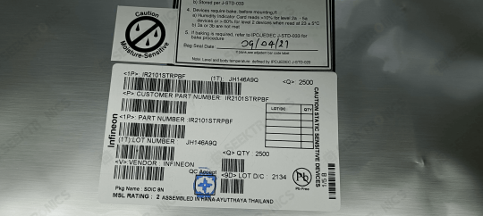
Today's delivery:IR2101STRPBF
Inquiry: [email protected]
Find more: www.seektronics.com
#Infineon#components#semiconductor#semiconductors#powerelectronics#chipshortage#electronics#powersupply#mcu#mosfet#igbt#electroniccomponents#electronicsmanufacturing#semiconductorindustry
0 notes
Text

DISTRIBUTORS OF SEMICONDUCTORS AND INDUSTRIAL COMPONENTS.
FOR MORE VISIT:
0 notes
Text
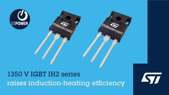
STMicroelectronics’ new IGBT brings better durability and efficiency
September 5, 2023 /SemiMedia/ — STMicroelectronics recently released a new series of IGBTs with improved breakdown voltage capability to 1350V and a maximum operating temperature of 175°C. The higher ratings ensure greater design margin, robust performance, and extended reliability under all operating conditions. The new STPOWER IH2 series IGBTs also permit increased power-conversion efficiency.…
View On WordPress
#25A STGWA25IH135DF2#electronic components news#Electronic components supplier#Electronic parts supplier#IGBT#STMicroelectronics
0 notes
Text
Choosing the Right Semiconductors for Stronger Circuits

In the dynamic world of electronics, making smart choices when selecting semiconductor components can greatly influence the performance and reliability of your projects. From microcontrollers to power transistors, each semiconductor plays a vital role in shaping the functionality of electronic devices.
Here are some simple yet crucial tips to consider when picking the right semiconductors:
Understanding Requirements: Begin by clearly defining your project's requirements. Consider factors like voltage, current, temperature range, and speed. This understanding will guide you toward components that best match your project's needs.
Application Consideration: Different semiconductor components are designed for specific applications. Opt for components that are purpose-built for your project type, whether it's digital, analog, or mixed-signal.
Datasheets Analysis: Thoroughly review the datasheets of potential components. Pay attention to parameters like maximum ratings, operating conditions, and performance characteristics. This helps ensure compatibility and optimal performance.
Availability and Lead Time: Check the availability and lead time of the components you're interested in. Delays in sourcing components can hinder project timelines.
Longevity and Support: Choose components from reputable manufacturers that offer long-term availability and reliable technical support. This prevents obsolescence issues down the line.
Cost-effectiveness: While it's important to choose quality components, also consider your budget. Balance performance and cost to achieve an efficient solution.
Future Scalability: Anticipate future upgrades or modifications. Select components that allow for scalability and easy integration with potential enhancements.
When it comes to sourcing your semiconductor components, consider Millennium Semiconductors as your reliable partner.
With a proven track record of providing top-quality components from renowned manufacturers, Millennium Semiconductors ensures access to a wide range of options to meet your project's unique requirements. Our commitment to customer satisfaction and technical expertise makes them the ideal choice for electronic enthusiasts and professionals alike.
Make your projects shine by making smart semiconductor choices through Millennium Semiconductors.
For more visit-
#millennium semiconductors#electronic components distributor#igbt power modules#lora module#millenniumsemi#Stronger Circuits
0 notes
Text
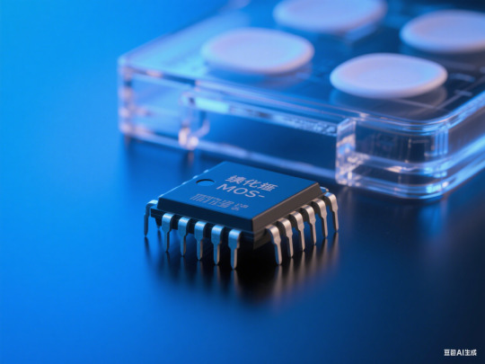
🔥 2025 MOS Electronics Deep Dive: The Tipping Point of Tech Disruption & Industry Reshaping 🔥

💥 Price Revolution! SiC MOSFETs Ignite Domestic Replacement Era 💥 Chinese IDM makers achieve historic breakthroughs: SiC MOSFET unit prices now undercut silicon-based IGBTs and super-junction MOSFETs at equivalent power ratings – a landmark "price inversion". Companies like BASiC Semiconductor slash module costs to 70% of imported solutions via 8-inch wafer mass production and vertical integration, boosting system efficiency by 15%. VBsemi amplifies this advantage with proprietary substrate-thinning and wafer-level testing, achieving 92% wafer utilization and 18% YoY cost reduction. Their SiC modules demonstrate 12% lower switching loss than global rivals in BYD’s 800V platform tests, fueling China’s transition from tech follower to cost leader. Projected 2025 SiC adoption: >30% in EVs, with rapid expansion in solar inverters and charging piles.
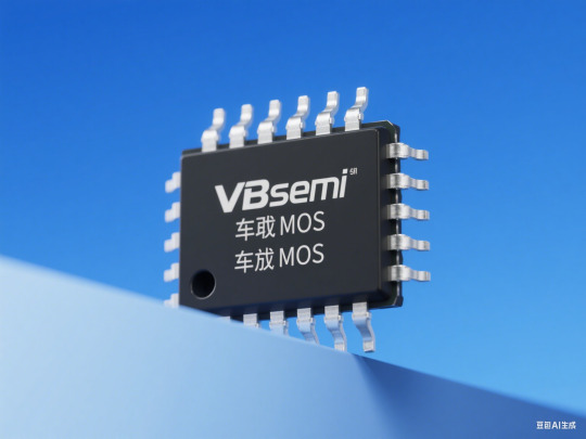
🚗 Automotive-Grade MOS Survival Thresholds: From AEC-Q101 to 800V Platforms 🚗 EV intelligence demands high-voltage/high-frequency solutions. Infineon’s OptiMOS™ 7 cuts RDS(on) by 25% and boosts switching speed by 20% using copper-clip packaging and 12-inch thin-wafer tech. BYD’s 2025 sourcing prioritizes diodes/transistors for power modules, while SemiDrive’s ASIL-D certified MCUs and GigaDevice’s GD32A503 secure major shares. VBsemi’s automotive MOS family, AEC-Q101 Grade 0 certified, features a tri-clad copper bonding structure reducing thermal resistance by 40%. Validated in XPENG’s brake-by-wire systems, it delivers millisecond response at -40°C with <10 PPM failure rates – setting new benchmarks for domestic reliability.
🌐 AI Compute Arms Race: DrMOS & Advanced Packaging Dual Fronts 🌐 NVIDIA’s GB300 NVL72 systems will drive 2025 DrMOS demand beyond 150M units, with AOS (70% share) as key supplier. NVIDIA’s cost-optimized 5x5mm DrMOS increases per-rack usage by 30% while halving unit prices, lifting server efficiency by 35%. TSMC’s CoWoS expansion and Chinese OSATs’ FOPLP/Chiplet projects push inter-chip bandwidth past 900GB/s. VBsemi’s next-gen DrMOS with Intelligent Phase Extension delivers 180A phase current in 5x5mm packages, accelerating dynamic response by 50%. Currently validating with Inspur, it boosts NVIDIA H100 GPU power efficiency by 0.8%, saving >$2,800/year per rack in electricity.
🌱 Circular Economy Reshapes Supply Chains: Recycling Boom to Lead-Free Wave 🌱 E-waste recycling surges in Shenzhen/Dongguan, with ICs fetching up to $23/PCS. EU’s 2026 lead-free mandate spurs demand for eco-components. VBsemi’s GreenMOS™ platform pioneers tin-whisker-resistant alloys and lead-free pre-plating, achieving 98% recyclability. Their super-junction MOS series passes IEC 61215 salt-mist certification, reducing coastal solar farm failures by 70%. BYD/CATL’s closed-loop systems target 85% material reuse by 2025.
🔋 Material Revolution: Silicon to Quantum Tunneling Breakthroughs 🔋 Third-gen semiconductors advance in parallel: TYSiC’s 8-inch SiC wavers hit 85% yield with 1.6% resistivity uniformity; Origin Quantum’s 72-qubit "Wukong" chip and IBM’s 1000-qubit processor mark quantum leaps. VBsemi’s hybrid gate-oxide tech (co-developed with CAS) slashes GaN HEMT gate leakage by 1,000x, enabling 97.2% efficiency at 2400V. Deployed in Huawei’s chargers, it achieves record 6.8W/cm³ power density.
💡 The Next Decade: From "China Replacement" to "Global Redefinition" 💡 Per BCG, 2025 global semiconductor market rebounds to $650B (AI chips +35%, consumer electronics +3%). China reconfigures supply chains via "wafer-fab origin" rules: SMIC’s 28nm capacity grows 5x in 3 years with 52% domestic equipment; JCET’s advanced packaging runs at >85% utilization. As Cambricon’s computing-in-memory chips rival global leaders and YMTC’s 128L NAND forces Samsung to cut prices by 15%, a multipolar tech era accelerates – with VBsemi’s innovations at its core.
👉 Follow #MOSElectronics #ChipRevolution #TechSovereignty for industry pulse!

#mosfet#semiconductor#electronics#mosfets#popular science animation#technology#circuit#electronic#munich#youtube
2 notes
·
View notes
Text
What is PCB Assembly ?
PCB Assembly manufacturer - Hitech Circuits Co., Limited
It’s the step in the manufacturing process in which you populate a blank board with the electronic components needed to make it into a functional printed circuit board. It’s these components that make a board into the circuit that enables an electronic product to function. PCB assembly typically takes place via one of two processes:
1. Surface-mount technology
SMT: SMT stands for “Surface Mount Technology“. The SMT components are very small sizes and comes in various packages like 0201, 0402, 0603, 1608 packages for resistors and capacitors. Similarly for Integrated circuits ICs we have SOIC, TSSOP, QFP and BGA.
The SMT components assembly is very difficult for human hands and can be time taking process so it is mostly done by automated pick and place machine.
2. Through-hole manufacturing
THT: THT stands for “Through hole Technology”. The components with leads and wires, like resistors, capacitors, inductors, PDIP ICs, transformers, transistors, IGBTs, MOSFETS are example.
The component has to be inserted on one side of PCB and pulled by leg on other side and cut the leg and solder it. The THT components assembly is usually done by hand soldering and is relatively easy.
Printed Circuit Board Assembly Techniques
There are only two common PCBA techniques available for use by a PCB designer. The methods are:
1. Automated PCB Assembly Techniques
Generally, this technique employs the use of state of the art machines, which are fully automatic. For example, the surface mount components are worth positioning with the aid of an automated pick and place machine.
Again, reflow soldering is commonly for surface mount components usually done in a reflow oven. An automated solder stencil is also used to apply the solder paste on the PCB.
Finally, high tech inspection machines are used to confirm and check the quality of the PCBA. Some of which include: Automated optical inspection machine (AOI), X-ray inspection machines, etc.
Above all, due to the precise monitoring, control of soldering, no human input and versatile machines.
This technique ensures utmost efficiency, output consistencies, and limits defects.
2. Manual PCB Assembly Techniques
This method is favorite for use with through-hole parts, which needs manual placement on the board. Besides, with these through-hole parts, it’s advisable you use wave soldering. Note that in the through- hole assembly process, you need to place the components and electronics on the PCB.
After that, you use wave soldering to solder the leads. Typically, you will need an individual to insert a component into a marked PTH. Once done, transfer the PCB to the next station where the next person will be on standby tasked with fixing another part.
What are the Benefits of SMT PCB Assembly?
SMT assembly provides many benefits and some of them are as follows:
It can be used to incorporate small components.
In SMT, the components can be placed on both sides of the board.
It assures high component densities.
Fewer holes need to be drilled for surface mounting than through-hole.
It require low initial costs and time for setting up the mass production.
SMT is the simpler and faster-automated assembly when compared to through-hole.
Errors regarding the component placement can be easily rectified.
Surface mount PCBs feature strong joints, which can easily withstand vibrations.
What are the techniques used in Surface Mount Technology?
There are several techniques for the reflow process. After applying the solder paste or a flux mixture on the board and after placing the components, the boards are conveyed to a reflow soldering oven. The techniques used for reflowing soldering include infrared lamps, hot gas convection, fluorocarbon liquids with a high boiling point, and so on.
What are the different testing methods used in SMT PCB Assembly?
Hitech Circuits as the PCB assembly manufacturer, we perform the following testing and inspection to ensure the quality of surface mount PCBs.
Automated Optical Inspection (AOI): This is performed before and after the soldering to identify the component placement, presence, and solder quality.
X-ray Testing: In this type of testing, the operator relies on the X-ray images of the PCB to check the solder joints and lead-less components such as Quad Flat Packs and ball grid arrays, which are generally not visible to naked eyes.
In-Circuit Testing (ICT): This method is used to detect manufacturing defects by testing the electrical properties in the SMT Assembly.
What type of files or documents should I send for SMT PCB Assembly?
Gerber Files: The file contains all details of physical board layers including solder masks, copper layers, drill data, legends, and so on.
Bill of Materials (BOM): This contains information on the list of items needed for the PCB manufacturing and the instructions of manufacturing.
Pick and Place File: This file contains information on all components to be used in the PCB design and their rotation and X-Y coordinates.
The whole process of PCB Assembly
1. Bare board loader machine
The first step in the PCB assembly is to arrange the bare boards on the rack, and the machine will automatically send the boards one by one into the SMT assembly line.
2. Printing solder paste
When PCB on the SMT production line, firstly, we have to print solder paste on it, and the solder paste will be printed on the pads of the PCB. These solder pastes will be melt and solder the electronic parts to the circuit board when it passes through the high-temperature reflow oven.
In addition, when testing new products, some people will use film board/adhesive cardboard instead of solder paste, which can increase the efficiency for adjusting the SMT machines.
3. Solder paste inspection machine(SPI)
Since the quality of solder paste printing is related to the quality of welding of subsequent parts, some SMT factories will use optical machine to check the quality of solder paste after printed the solder paste in order to ensure stable quality. If there any poorly printed solder paste board, we will wash off the solder paste on it and reprint, or remove the excess solder paste if there is redundant solder paste on it.
4. High speed SMT machine
Usually, we will put some small electronic parts (such as small resistors, capacitors, and inductors) to be printed on the circuit board first, and these parts will be slightly stuck by the solder paste just printed on the circuit board, so even if the speed of printing is very fast and the parts on the board will not fall away. But large parts are not suitable for use in such high speed SMT machines, which will slow down the speed of small parts assembly. And the parts will be shifted from the original position due to the rapid movement of the board.
5. Universal SMT machine
Universal SMT machine is also known as "slow machine", it will be assembled some large electronic components, such as BGA IC, connectors, etc., these parts need more accurate positions, so the alignment is very important. Use a camera to take a picture to confirm the position of the parts, so the speed is much slower than High speed SMT machine we taked before. Due to the size of the components here, not all of them are packed in tape and reel, and some may be packed in trays or tubes. But if you want the SMT machine to recognize the trays or tube-shaped packaging materials, you must configure an additional machine.
Generally, traditional SMT machines are using the principle of suction to move electronic parts, and in order to place the parts successfully, and there must be the flat surface on these electronic components for the suction nozzle of the SMT machine to absorb. However, for some electronic parts don’t have a flat surface for these machines, and it is necessary to order special nozzles for these special-shaped parts, or add a flat tape on the parts, or wear a flat cap for thees electronic parts.
6. Manual parts or visual inspection
After assembled all parts by the high speed SMT machine or Universal SMT machine and before going through the high-temperature reflow oven, and we will set up a visual inspection station here and to pick out the deviation parts or missing components boards etc., because we have to use a soldering iron to repair if there are still defectives boards after passing the high-temperature oven, which will affect the quality of the product and will also increase the cost. in addition, for some larger electronic parts or traditional DIP parts or some special reasons cannot be processed by the SMT machine before, they will be manually placed on pcb here.
7. Reflow oven
The purpose of reflow oven is to melt the solder paste and form a non-metallic compound on the component feet and the circuit board, that means to solder electronic components on the circuit board. The temperature rise and fall curves often affect the soldering quality of the entire circuit board. According to the characteristics of the solder materials, usually the reflow oven will set the preheating zone, soaking zone, reflow zone, and cooling zone to achieve the best soldering effect.
For example, the melting point for SAC305 solder paste with lead-free is about 217°C, which means that the temperature of the reflow oven must be higher than the melting points to remelt the solder paste. What's more, the maximum temperature in the reflow furnace should not exceed 250°C, otherwise many parts will be deformed or melted because they cannot withstand such a high temperature.
Basically, after the pcb passed through the reflow oven, the assembly for the entire circuit board is almost complete. If there are hand-soldered parts, we need to transfer to DIP process, and then we have to check the quality after reflow oven by QC department.
8. Automatic optical inspection(AOI)
The main purpose of setting up AOI is because some high density boards can’t be process the following ICT test, so we used AOI inspection to replace it. But even using AOI inspections, there still have the blind spots for such checking, for example, the solder pads under the components cannot be checked by AOI. At present, it can only check whether the parts have side standing issue, missing parts, displacement, polarity direction, solder bridges, lack of soldering etc., but cannot checking the BGA solderability, resistance value, capacitance value, inductance value and other components quality, so far AOI inspection can’t completely replace ICT test.
Therefore, there is still some risk if only AOI inspection is used to replace ICT testing, but ICT test is also not 100% make sure the good quality, we suggest these two ways can be combined with together to make sure the good quality.
9. PCB unloader machine
After the board is fully assembled, it will be retracted to the unloder machine, which has been designed to allow the SMT machine to automatically pick and place the board without damaging the quality for PCB.
10. Visual inspection for finished products
Normally there will be a visual inspection area in our SMT production line whether there is an AOI station or not, and it will help to check if there are any defectives after completed assembled the pcbs. If there is an AOI station, it can reduce the visual inspection worker on our SMT line, and to reduce the potential cost, and because it is still necessary to check some places that cannot be judged by AOI, many SMT factories will provide the mainly visual inspection templates at this station, which is convenient for visual inspection worker to inspect some key parts and polarity for components.
11. DIP process
DIP process is a very important process in the whole PCBA processing, and the processing quality will directly affect the functional for PCBA boards, so it is necessary to pay more attention to the DIP process. There are many preliminary preparations for DIP process. The basic process is to re-process the electronic components first, like to cut the extra pins for some DIP components, our staff received the components according to the BOM list, and will check whether the material part numbers and specifications are correct or not, and performs pre-production pre-processing according to the PCBA samples. The steps are: Use various related equipment (automatic capacitor pins cutting machine, jumper bending machine, diode and triode automatic forming machine, automatic belt forming machine and other machines) for processing.

12. ICT test
Printed Circuit board open/short circuit test (ICT, In-Circuit Test), The purpose of ICT test is mainly to test whether the components and circuits on the printed circuit board are open or short issues. It can also measure the basic characteristics of most components, such as resistance, capacitance, and inductance values to judge whether the functions of these parts are damaged, wrong parts or missing parts etc. after passing through the high-temperature reflow oven.
ICT test machines are divided into advanced and basic machines. The basic ICT test machines are generally called MDA (Manufacturing Defect Analyzer). It’s just to measure the basic characteristics of electronic components and judge open and short circuits issue we talked above.
In addition to all the functions of the basic ICT test machines, for advanced ICT test machine can also test the whole PCBA by using power, start to testing the PCBA boards by setting the program in the test machine. The advantage is that it can simulate the function of the printed circuit board under the actual power-on condition, this test can partly replace the following functional test machine (Function Test). But the cost for the test fixture of this advanced ICT test can probably buy a car, it’s too expensive and we suggest it can be used in mass production products.
13. PCBA function test
Functional testing is to make up for the ICT test, because ICT only tests the open and short circuits on the the PCBA board, and other functions such as BGA and other fuctions are not tested, so it is necessary to use a functional testing machine to test all functions on the whole PCBA board.
14. Cutting board (assembly board de-panel)
Normally, printed circuit boards will be produced in panel, and it will be assembled to increase the efficiency of SMT production. It means several single boards in one panel, such as two-in-one, four-in-one etc. After finished all the pcb assembly process, it needs to be cut into single boards, and for some printed circuit boards with only single boards also need to cut off some redundant board edges.
There are several ways to cut the printed circuit board. You can design the V-cut using the blade cutting machine (Scoring) or directly manually break off the board (not recommended). For more high density circuit boards, it will be used the professional splitting machine or the router to split the board without any damage the electronic components and printed circuit boards, but the cost and working hours will be a little longer.
Why Choose Hitech Circuits PCB Assembly Manufacturer for Your PCB Assembly Projects?
There are several PCB manufacturers specializing in PCB assemblyservices. However, Hitech Circuits PCB Assembly stands out owing to the following:
Assistance in Material Procurement:
Technically, in PCB assembly services, the quality of parts is the responsibility of the OEM; however, we ease your job by assisting you to make the right selection. We can help you procure all your parts of the same type own a single part number, thanks to our supply chain and vendor network as well as experience. This saves time and cost that goes in ordering single parts as you plan.
Testing procedures:
We are very focused on quality and thus implement stringent testing procedures at each stage of the assembly and after completion.
Fast Turnaround Times:
Our well-equipped facility and the right tools enable us to complete your requirements well before time, and without compromising on the quality or functioning of the PCBs. For simple designs we revert in 24 to 48 hours.
Cost Effectiveness:
While PCB assembly is a cost-effective alternative, we go a step further and assure that the parts you list are of a good quality and suitable for your requirement. Also, you can control the part flow and replenish them as needed. This eliminates the need to buy extra stock and store it.
Quick Quote:
We offer a quick quote based on your BOM. All you need is a detailed BOM, Gerber files, your application requirement sheet, and quantity.
We’re not one to stand still, which is why we use the latest equipment and the finest minds to create your PCB projects. We’re constantly keeping our finger on the pulse of the latest trends. And as a result, we know how to deliver the highest standards of PCB assembly to meet all your requirements.
Our dedicated, friendly customer service team also means that we support you every step of the way. Offering our expert guidance to ensure a complete PCB project that you’re happy with.
Contact us today
No matter what your printed circuit board assemblyneeds are, we always aim to deliver efficient, dependable solutions. For more information about our services, do not hesitate to get in touch with us today for a no-obligation quote
2 notes
·
View notes
Text
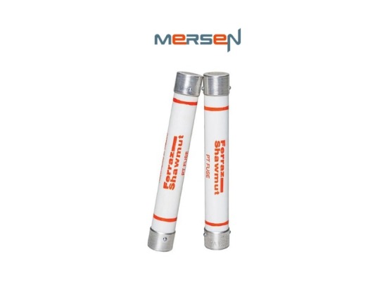
Understanding Protistor Fuses and the PT Fuse 9F60 Series: High-Performance Protection for Power Electronics
In the field of electrical engineering and power electronics, ensuring circuit protection and equipment safety is of paramount importance. Among the most trusted components in this domain areProtistor fuses—specifically, the Protistor size 33 aR, Protistor size 32 aR, E Rated fuses, and the advanced PT fuse 9F60 series. These fuses are essential for safeguarding semiconductor devices such as IGBTs, diodes, and thyristors against overcurrents and short circuits.
Protistor Size 32 aR and Size 33 aR – Fast-Acting Precision
The Protistor size 32 aR and Protistor size 33 aR are ultrafast fuses specifically designed for semiconductor protection. These fuses are part of the “aR” category—meaning they provide partial range protection and are intended to protect only against short circuits, not overloads.
Size 32 aR Fuses typically come with voltage ratings around 690V AC and offer current ratings from 10A to 1000A. Their compact design and quick response make them ideal for power converters and rectifier bridges.
Size 33 aR Fuses provide similar protection but are designed for applications requiring slightly higher interrupting capacity or different mechanical dimensions.
These fuses utilize a silver fuse element and low arc voltage, enabling minimal energy let-through during fault conditions. Their ability to interrupt high fault currents with minimal damage makes them indispensable in high-speed power electronics environments.
E Rated Fuses – Industrial Power System Standards
E Rated fuses are standardized per ANSI C37.46 and are typically used in medium-voltage distribution systems. The “E” classification means the fuse has a defined melting time for a given multiple of current (e.g., E-rated fuses must melt in 300 seconds at 200% of rated current). They are suitable for general-purpose protection of transformers, capacitors, and medium-voltage motors.
These fuses provide both short-circuit and overload protection, making them versatile in industrial applications. E Rated fuse are not as fast-acting as aR fuses, but their broader protection range makes them ideal for general medium-voltage use.
PT Fuse 9F60 Series – Next-Level Protection
The PT fuse 9F60 series is a specialized series of high-performance fuses engineered by trusted manufacturers like Mersen. These fuses are designed for photovoltaic (solar) systems, UPS, industrial drives, and power supplies that require protection of DC and AC circuits.
Key features of the 9F60 series include:
Ultra-fast acting characteristics for protecting sensitive semiconductor components.
Ratings typically up to 1000V DC or more.
High interrupting capacity and excellent cycling capability.
Compact and robust design with easy installation.
These fuses meet both IEC and UL standards, ensuring global compatibility and reliability in critical systems.
Conclusion
Whether you're working with high-speed semiconductor devices or industrial power systems, selecting the right fuse is essential. The Protistor size 32 aR and size 33 aR offer lightning-fast protection for sensitive electronics. The E Rated fuses provide robust and standardized overload and short-circuit protection, while the PT fuse 9F60 series represents the pinnacle of high-performance fuse technology for modern, high-demand applications.
0 notes
Text
Ceramic Electronic Substrates Market: Strategic Analysis of Key Players and Regions 2025–2032
Ceramic Electronic Substrates Market, Global Outlook and Forecast 2025-2032
Ceramic Electronic Substrates Market was valued at US$ 3.76 billion in 2024 and is projected to reach US$ 5.84 billion by 2032, at a CAGR of 5.67% during the forecast period 2025-2032
Our comprehensive Market report is ready with the latest trends, growth opportunities, and strategic analysis https://semiconductorinsight.com/download-sample-report/?product_id=88028
MARKET INSIGHTS
The global Ceramic Electronic Substrates Market was valued at US$ 3.76 billion in 2024 and is projected to reach US$ 5.84 billion by 2032, at a CAGR of 5.67% during the forecast period 2025-2032. The U.S. market is estimated at USD 320 million in 2024, while China is expected to reach USD 580 million by 2031, driven by expanding electronics manufacturing capabilities.
Ceramic electronic substrates are specialized materials that provide mechanical support and electrical insulation for semiconductor devices. These high-performance substrates, including alumina (Al₂O₃), aluminum nitride (AlN), and silicon nitride (Si₃N₄) variants, enable efficient heat dissipation and stable performance in demanding applications. Their unique properties make them essential for LED packaging, power electronics, and high-frequency communication systems.
The market growth is fueled by increasing demand for advanced electronics, particularly in electric vehicles and 5G infrastructure, where thermal management is critical. The alumina segment currently dominates with over 65% market share, while AlN substrates are gaining traction due to superior thermal conductivity. Key players like Kyocera, CoorsTek, and CeramTec are expanding production capacities to meet rising demand, particularly in Asia-Pacific where electronics manufacturing is concentrated.
List of Key Ceramic Electronic Substrate Companies Profiled
CoorsTek (U.S.)
Maruwa Co., Ltd. (Japan)
Toshiba Materials Co., Ltd. (Japan)
CeramTec GmbH (Germany)
Denka Company Limited (Japan)
Kyocera Corporation (Japan)
Japan Fine Ceramics Co., Ltd. (Japan)
NCI Company (Japan)
Hitachi Metals, Ltd. (Japan)
Leatec Fine Ceramics Co., Ltd. (Taiwan)
Fujian Huaqing Electronic Material Technology Co., Ltd. (China)
Wuxi Hygood New Technology Co., Ltd. (China)
Ningxia Ascendus (China)
Shengda Tech (China)
Chaozhou Three-Circle (Group) Co., Ltd. (China)
Leading Tech (China)
Segment Analysis:
By Type
Alumina Electronic Substrates Lead Market Share Due to Cost-Effectiveness and High Thermal Conductivity
The market is segmented based on type into:
Alumina Electronic Substrates
AlN Electronic Substrates
Key features: Excellent thermal conductivity and electrical insulation
Silicon Nitride Electronic Substrates
Key features: High mechanical strength and thermal shock resistance
By Application
LED Segment Holds Largest Market Share Due to Extensive Use in Lighting Solutions
The market is segmented based on application into:
LED
Chip Resistor
IGBT Module
Optical Communication
Aerospace
Others
By End User
Electronics Industry Dominates Consumption Due to Growing Demand for Miniaturized Components
The market is segmented based on end user into:
Consumer Electronics
Automotive Electronics
Industrial Electronics
Telecommunications
Aerospace & Defense
Regional Analysis: Ceramic Electronic Substrates Market
North America The North American market for ceramic electronic substrates is driven by strong demand from the aerospace, defense, and telecommunications sectors. The U.S. leads the region, accounting for over 70% of the market share, supported by significant investments in advanced electronics manufacturing. Companies like CoorsTek and CeramTec dominate the supply chain, focusing on high-performance alumina and aluminum nitride (AlN) substrates for applications in 5G infrastructure and EVs. Stringent quality standards and a push for miniaturization in electronics are key growth drivers. However, high production costs and competition from Asian manufacturers remain challenges for local players.
Europe Europe’s ceramic substrates market is characterized by strict regulatory compliance and innovation in materials science. Germany, France, and the U.K. are major contributors, with Kyocera and CeramTec leading product development. The region shows strong demand for AlN substrates due to their superior thermal conductivity in automotive and industrial applications. The EU’s focus on reducing electronic waste and promoting green manufacturing is accelerating the adoption of sustainable ceramic solutions. However, sluggish growth in traditional sectors like consumer electronics has slightly tempered market expansion in recent years.
Asia-Pacific Asia-Pacific dominates the global ceramic substrates market, contributing over 50% of total revenue, with China, Japan, and South Korea as key hubs. China’s aggressive expansion in semiconductor and LED manufacturing has fueled demand, supported by domestic players such as Chaozhou Three-Circle. Japan remains a technology leader, with Maruwa and Toshiba Materials specializing in high-purity substrates for automotive electronics. While cost competitiveness drives volume growth, the region is also investing in R&D for next-gen silicon nitride substrates to cater to the aerospace sector. India and Southeast Asia are emerging markets, albeit constrained by limited local manufacturing capabilities.
South America South America’s ceramic substrates market is nascent but growing, primarily driven by Brazil’s automotive and energy sectors. The lack of domestic production means heavy reliance on imports from North America and Asia, which inflates costs. Argentina and Chile show modest demand for substrates in consumer electronics and renewable energy applications. Infrastructure gaps and economic instability, however, hinder large-scale investments in advanced electronics manufacturing, keeping the region a minor player in the global market.
Middle East & Africa The Middle East & Africa market is emerging, with growth concentrated in the UAE, Saudi Arabia, and South Africa. Demand is fueled by telecom infrastructure projects and oil & gas sector applications requiring high-temperature-resistant substrates. While the region lacks local manufacturers, partnerships with global suppliers like Kyocera are gradually expanding market access. Africa’s potential remains untapped due to limited industrialization, though increasing foreign investments in electronics assembly could drive future demand for ceramic substrates.
MARKET DYNAMICS
As electronic devices continue shrinking, ceramic substrates face inherent physical limitations that challenge further miniaturization. The brittleness of traditional alumina substrates makes them difficult to process below certain thickness thresholds, limiting their use in cutting-edge wearable devices and ultra-compact electronics. While newer materials like silicon nitride show promise with improved mechanical properties, their adoption remains constrained by processing complexities and higher costs. The industry must overcome these material science challenges to maintain competitiveness against emerging organic and composite substrate alternatives that offer greater design flexibility for compact applications.
Ceramic substrates face intensifying competition from advanced organic substrates and direct bonded copper technologies that continue improving their thermal performance. These alternatives are gaining traction in mid-range power applications where their lower costs and design flexibility outweigh the thermal advantages of ceramics. The development of thermally conductive polymers with thermal conductivities approaching 20 W/mK further threatens traditional ceramic substrates in certain applications. Market participants must differentiate their offerings through performance enhancements and application-specific solutions to maintain technological leadership in this evolving competitive landscape.
The aerospace and defense sector presents significant growth potential for high-performance ceramic substrates, particularly for radar systems and satellite communications where reliability under extreme conditions is paramount. The unique combination of high thermal conductivity and low dielectric loss makes ceramic substrates ideal for these demanding applications. With global defense spending expected to exceed $3 trillion by 2031 and increasing emphasis on electronic warfare capabilities, manufacturers have opportunities to develop specialized substrate solutions that meet stringent military specifications while achieving the performance characteristics required for next-generation systems.
The rapid growth of renewable energy infrastructure is creating substantial demand for robust power electronic solutions utilizing ceramic substrates. Solar inverters and wind turbine converters increasingly incorporate high-power IGBT modules that rely on ceramic substrates for thermal management. With global renewable capacity additions projected to grow at 12% CAGR through 2030, substrate manufacturers can capitalize on this trend by developing solutions optimized for the specific requirements of energy conversion systems. This includes substrates capable of withstanding the harsh environmental conditions typical in renewable energy installations while maintaining long-term reliability.
The evolving needs of advanced electronics are driving unprecedented collaboration between substrate manufacturers, semiconductor companies, and end-users to develop next-generation solutions. These partnerships aim to create substrate materials with tailored thermal and electrical properties for specific applications, from wide bandgap semiconductors to high-frequency RF devices. Recent developments include ceramic-metal composite substrates that combine the thermal performance of ceramics with the mechanical advantages of metals. Such innovations, enabled by collaborative R&D efforts, are expected to open up new application areas and drive the next phase of market growth in high-value segments.
The market is highly fragmented, with a mix of global and regional players competing for market share. To Learn More About the Global Trends Impacting the Future of Top 10 Companies https://semiconductorinsight.com/download-sample-report/?product_id=88028
FREQUENTLY ASKED QUESTIONS:
What is the current market size of Global Ceramic Electronic Substrates Market?
Which key companies operate in Global Ceramic Electronic Substrates Market?
What are the key growth drivers?
Which region dominates the market?
What are the emerging trends?
CONTACT US: City vista, 203A, Fountain Road, Ashoka Nagar, Kharadi, Pune, Maharashtra 411014 [+91 8087992013] [email protected]
0 notes
Text
Handheld Imager Market Size Empowering Precision Scanning Across Industries
The Handheld Imager Market is witnessing a significant rise in global demand, driven by industries embracing advanced imaging solutions for enhanced operational efficiency, safety, and data accuracy. These portable, high-performance devices are revolutionizing tasks ranging from industrial inspections to law enforcement and healthcare diagnostics.
Market Overview
Handheld imagers are portable devices equipped with optical, thermal, or X-ray sensors, allowing users to capture real-time images or detect hidden structures in various materials. Their compact design and ease of use make them an ideal tool for applications where mobility and immediate feedback are critical.
As industries digitize and prioritize smart, connected operations, the role of handheld imaging systems becomes increasingly essential. From building inspections to homeland security and maintenance of electrical systems, these devices are empowering professionals with fast, accurate, and detailed imaging capabilities.
Key Market Drivers
Increased Demand for Non-Destructive Testing (NDT): Industries like oil & gas, aerospace, and automotive are adopting handheld imagers for routine inspections to ensure safety and compliance without damaging components.
Rising Security and Surveillance Applications: Law enforcement, border control, and security agencies are using handheld thermal imagers to detect hidden objects or monitor activities in low visibility conditions.
Growth in Healthcare Imaging: Handheld ultrasound and infrared thermography devices are being adopted for point-of-care diagnostics and quick screening, particularly in remote areas.
Industrial Automation & Smart Maintenance: Maintenance professionals are using thermal handheld imagers to detect equipment anomalies, enabling predictive maintenance and reducing downtime.
Market Segmentation
By Technology: Thermal, Terahertz, Optical, X-ray
By Application: Industrial, Security, Healthcare, Construction, Law Enforcement
By End-User: Commercial, Military, Government, Medical
By Region: North America, Europe, Asia-Pacific, Latin America, Middle East & Africa
Regional Insights
North America leads the market, with high adoption across security, infrastructure, and industrial sectors.
Asia-Pacific is the fastest-growing region, driven by increased investments in manufacturing, smart cities, and defense modernization.
Europe remains a stable market with continued innovations in portable medical and industrial imaging tools.
Competitive Landscape
Leading companies operating in the handheld imager market include:
FLIR Systems (Teledyne Technologies)
Testo SE & Co.
BAE Systems
Fluke Corporation
Leonardo S.p.A.
Opgal Optronic Industries
These companies are focusing on enhancing resolution, battery life, connectivity features, and multi-spectral capabilities to gain market share and address evolving customer needs.
Trending Report Highlights
Explore more insights from top-performing sectors with the latest Market Research Future reports:
IGBT Market
Thermal Management Market
Smart Mirror Market
Optical Lenses Market Research Report - Global Forecast 2030
Hi-Fi Speaker System Market
Connected IoT Devices Market
GaAs Wafer Market
Linear Motor Market
Multi-Vendor Support Services Market
Microprocessor and GPU Market Research Report – Global Forecast till 2030
Predictive Emission Monitoring System (PEMS) Market
Soft Robotics Market
0 notes
Text
youtube
Toshiba MG200J1ZS50 IGBT Module – 600V 200A High-Power Transistor | Shop at USComponent
Visit https://www.uscomponent.com/buy/Toshiba/MG200J1ZS50.
The Toshiba MG200J1ZS50 is a powerful, high-current IGBT module engineered for demanding industrial and high-power switching applications. Rated at 600V and 200A, this insulated-gate bipolar transistor module is ideal for use in motor drives, welding equipment, induction heating systems, power inverters, and other high-frequency power control systems. With its fast switching capability and low saturation voltage, the MG200J1ZS50 is optimized for both performance and efficiency under heavy load conditions.
Built with Toshiba’s renowned IGBT technology, this module ensures high-speed operation, low conduction loss, and superior thermal stability. Its isolated baseplate supports better heat dissipation and enhances safety by providing electrical insulation between the module and the heatsink. This not only increases reliability in high-voltage environments but also simplifies mechanical design. Whether you're performing a system upgrade or replacing a failed component, the MG200J1ZS50 Toshiba IGBT Module offers the robust performance and proven durability that industrial users depend on.
At USComponent, we are proud to be an authorized Toshiba distributor of genuine IGBT modules. When you purchase the MG200J1ZS50 from us, you can be assured of receiving only brand-new, factory-sealed components, backed by expert technical support, fast international shipping, and highly competitive pricing. Don’t compromise your systems with unverified parts—choose USComponent to order the Toshiba MG200J1ZS50 today and ensure your application runs with confidence and power.
#IGBT#IGBT Module#IGBT Power Module#IGBT Transistor#Semiconductor Toshiba#IGBT Inverter#IGBT Distributor#Toshiba Electronic Components#IGBT Power#IGBT Module Manufacturers#IGBT Module Price#High Power IGBT#IGBT Suppliers#Toshiba Semiconductor Distributors#Toshiba MG200J1ZS50#Tosiba IGBT Module#Toshiba IGBT#Youtube
0 notes
Text

Today's delivery:SGM3001XC6TR
Inquiry: [email protected]
Find more: www.seektronics.com
#SGMicro#components#semiconductor#semiconductors#powerelectronics#chipshortage#electronics#powersupply#mcu#mosfet#igbt#electroniccomponents#electronicsmanufacturing#semiconductorindustry#electronicshop
0 notes
Text
Gate Driver Board Market : Industry Size, Share Trends, Growth, Demand, Opportunities and Global Forecast to 2032
The global Gate Driver Board market size was valued at US$ 1.23 billion in 2024 and is projected to reach US$ 2.01 billion by 2032, at a CAGR of 7.45% during the forecast period 2025–2032. The U.S. market accounted for approximately 25% of global revenue in 2024, while China is expected to witness the fastest growth at 9.1% CAGR through 2032.
Gate Driver Boards are critical components in power electronics that control the switching of semiconductor devices like IGBTs, MOSFETs, and SiC modules. These boards provide the necessary voltage and current to drive power switches efficiently while ensuring protection against short circuits, overcurrent, and overheating. The market comprises three key product types: SiC Gate Driver Boards (fastest growing segment), MOSFET Gate Driver Boards, and IGBT Gate Driver Boards.
The market growth is primarily driven by increasing adoption of electric vehicles, renewable energy systems, and industrial automation. The SiC segment is particularly gaining traction due to its superior efficiency in high-voltage applications. Key players including Infineon Technologies, STMicroelectronics, and ON Semiconductor are investing heavily in R&D to develop advanced gate driver solutions. For instance, in Q1 2024, Infineon launched a new generation of galvanically isolated gate drivers with enhanced protection features for automotive applications.
Get Full Report with trend analysis, growth forecasts, and Future strategies : https://semiconductorinsight.com/report/gate-driver-board-market/
Segment Analysis:
By Type
SiC Gate Driver Board Segment Leads Due to High Efficiency in Power Electronics
The market is segmented based on type into:
SiC Gate Driver Board
MOSFET Gate Driver Board
IGBT Gate Driver Board
Others
By Application
Automotive Sector Dominates Market Share Due to Rising EV Adoption
The market is segmented based on application into:
Automobile
Motor
Home Appliances
Others
By Voltage Range
High Voltage Segment Gains Traction for Industrial Power Systems
The market is segmented based on voltage range into:
Low Voltage
Medium Voltage
High Voltage
By Isolation Type
Optocoupler-based Isolation Preferred for Enhanced Safety Requirements
The market is segmented based on isolation type into:
Optocoupler-based
Magnetic Isolation
Capacitive Isolation
None-Isolated
Regional Analysis: Gate Driver Board Market
North America The North American gate driver board market is driven by advanced semiconductor manufacturing and strong demand from electric vehicle (EV) and industrial automation sectors. The U.S. accounts for over 60% of regional revenue, supported by major players like Infineon Technologies and Microchip Technology. Robust investments in 5G infrastructure and renewable energy systems further propel the adoption of SiC-based gate driver boards, with the U.S. Department of Energy allocating $3 billion for next-gen power electronics research. However, supply chain disruptions and geopolitical trade tensions pose challenges for manufacturers sourcing components from overseas.
Europe Europe’s market growth is fueled by stringent energy efficiency regulations like EU Ecodesign Directives, pushing industrial and automotive sectors toward optimized power devices. Germany dominates with its strong automotive OEM base, while Nordic countries lead in renewable energy applications. The region shows increasing preference for isolated gate driver solutions to meet safety standards in high-voltage applications. European manufacturers face margin pressures due to rising raw material costs but maintain technological leadership through R&D collaboration between academia and industry.
Asia-Pacific Accounting for 42% of global gate driver board consumption, the Asia-Pacific market is propelled by China’s massive electronics manufacturing sector and India’s growing EV industry. China’s semiconductor self-sufficiency initiatives have boosted local players like TARAZ TECHNOLOGIES, while Japan maintains dominance in high-reliability industrial applications. Price sensitivity drives demand for cost-effective MOSFET driver solutions, though premium segments show strong uptake in advanced manufacturing and energy storage systems. Infrastructure challenges and intellectual property concerns remain barriers for international suppliers.
South America The region presents nascent but promising opportunities, particularly in Brazil’s motor drives and Argentina’s renewable energy sectors. Limited local production capacity creates import dependency, with most gate driver boards sourced from Asia and North America. Growth is constrained by economic instability and fragmented regulatory environments, though increasing foreign investments in mining electrification and smart grid projects create pockets of demand. Suppliers must balance cost competitiveness with the need for ruggedized designs suitable for challenging operating conditions.
Middle East & Africa Market development in this region follows infrastructure modernization programs, particularly in Gulf Cooperation Council (GCC) countries. The UAE and Saudi Arabia drive demand through smart city initiatives and oil/gas industry automation. Africa shows potential in off-grid solar applications but faces adoption barriers due to limited technical expertise and after-sales support networks. While the market remains small compared to other regions, strategic partnerships with local distributors enable global players to establish footholds for long-term growth.
MARKET OPPORTUNITIES
Wide-Bandgap Semiconductor Revolution Creating Next-Generation Demand
Silicon carbide (SiC) and gallium nitride (GaN) technologies are transforming power electronics, with the SiC power module market expected to grow at 34% CAGR through 2030. These advanced semiconductors operate at higher temperatures, voltages, and frequencies than traditional silicon, requiring completely reimagined gate driver architectures. Manufacturers developing specialized GDBs for wide-bandgap applications can command 40-60% price premiums over conventional solutions.
Intelligent Gate Drivers Opening New Value Propositions
The integration of embedded processors and AI-based predictive algorithms creates opportunities for intelligent gate drivers that can self-optimize performance. Modern solutions now incorporate real-time health monitoring sensors that predict semiconductor degradation with 90%+ accuracy up to 1000 hours before failure. This capability is particularly valuable for mission-critical industrial systems where unplanned downtime costs exceed $260,000 per hour in some verticals. As Industry 4.0 adoption accelerates, smart gate drivers with IIoT connectivity will become standard requirements rather than premium options.
Moreover, the renewable energy sector’s rapid expansion presents untapped potential. Solar microinverter architectures alone are projected to drive demand for 25 million specialized gate driver units annually by 2027, as installers seek solutions that maximize energy harvest while withstanding harsh environmental conditions.
MARKET CHALLENGES
Thermal Management Constraints Limiting Power Density Improvements
While power semiconductor technology advances rapidly, thermal dissipation remains a stubborn bottleneck. Modern gate drivers must operate reliably at junction temperatures exceeding 175°C in automotive applications, pushing conventional packaging materials to their limits. Even with advanced cooling techniques, thermal resistance between semiconductor dies and heat sinks frequently exceeds 0.5°C/W – a significant constraint when dealing with multi-kilowatt power stages.
Other Critical Challenges
EMI/EMC Compliance Complexities The faster switching speeds enabled by modern GDBs generate significant electromagnetic interference, with common-mode noise often exceeding 100dBµV without careful mitigation. Meeting stringent automotive and medical EMC standards requires sophisticated board layouts and filtering techniques that add 15-20% to development costs.
Safety Certification Hurdles Achieving necessary safety certifications (such as IEC 62368-1 for reinforced isolation) demands extensive testing and documentation. The process typically adds 6-9 months to product development cycles and requires specialized test equipment costing upwards of $500,000 per setup.
GATE DRIVER BOARD MARKET TRENDS
Growing Electric Vehicle Adoption Fueling Demand for Gate Driver Boards
The rapid expansion of electric vehicle (EV) production globally has emerged as a primary driver for the gate driver board market. These components play a critical role in power semiconductor switching applications, particularly in EV inverters that convert DC battery power to AC for motor control. With annual EV sales projected to exceed 40 million units by 2030, manufacturers are scaling up production of high-performance gate drivers capable of handling silicon carbide (SiC) and gallium nitride (GaN) power devices. The automotive segment currently accounts for over 35% of total gate driver demand, a share expected to grow as legacy automakers accelerate their electrification roadmaps.
Other Trends
Shift Toward Wide Bandgap Semiconductors
The transition from traditional silicon-based to wide bandgap semiconductor technologies is reshaping gate driver requirements. SiC and GaN devices offer superior efficiency in high-power applications but demand specialized driver circuits with fast switching capabilities and robust protection features. This technological shift has prompted leading suppliers like Infineon and STMicroelectronics to develop dedicated gate driver IC families supporting switching frequencies above 100 kHz. The SiC gate driver segment alone is forecast to grow at a 25% CAGR through 2030, outpacing the overall market as renewable energy and industrial applications adopt these advanced power solutions.
Industrial Automation Driving Innovation
Expanding industrial automation across manufacturing sectors continues to fuel demand for reliable motor control solutions incorporating gate driver technology. Modern robotics, CNC machinery, and servo systems increasingly utilize intelligent gate drivers with integrated diagnostics and protection circuits. The growing emphasis on predictive maintenance in Industry 4.0 environments has led to the development of driver boards with real-time monitoring capabilities for parameters like gate voltage and temperature. As factory automation investments are projected to grow by 12% annually, gate driver manufacturers are focusing on ruggedized designs capable of withstanding harsh industrial environments while ensuring precise power device control.
Miniaturization Challenges Emerging
While performance requirements intensify, size constraints in modern electronics are pushing gate driver designers to balance functionality with compact form factors. The proliferation of portable medical devices and IoT equipment has created demand for space-efficient driver solutions, prompting innovations in packaging technologies and system-on-chip integration. However, thermal management remains a critical challenge as higher power densities can compromise reliability. Leading suppliers are addressing this through advanced isolation techniques and embedded thermal protection circuits, enabling smaller footprints without sacrificing robustness in mission-critical applications.
COMPETITIVE LANDSCAPE
Key Industry Players
Technological Innovation and Strategic Alliances Define Market Leadership
The global gate driver board market features a robust competitive environment with both established semiconductor giants and specialized technology providers vying for market share. Infineon Technologies emerges as a dominant force, leveraging its extensive R&D capabilities and comprehensive portfolio of power semiconductor solutions. The company’s recent advancements in silicon carbide (SiC) gate driver technology have particularly strengthened its position in high-growth sectors like electric vehicles and renewable energy systems.
STMicroelectronics and Analog Devices hold significant market positions, capturing approximately 22% of the global revenue share combined in 2024. Their competitive edge stems from vertically integrated manufacturing capabilities and strong partnerships with automotive OEMs. While Analog Devices excels in precision signal processing solutions, STMicroelectronics has made notable strides in intelligent power module integration.
Meanwhile, Japanese firm Toshiba demonstrates formidable expertise in IGBT driver technology, particularly for industrial motor drives. The company has been aggressively expanding its production capacity in Southeast Asia to meet growing regional demand. ROHM Semiconductor complements this landscape with its innovative GaN-based driver solutions, carving out a niche in high-frequency power conversion applications.
Emerging players like TARAZ TECHNOLOGIES and EgrTech are disrupting traditional market dynamics through specialized solutions for niche applications. Their agility in custom design services and faster time-to-market for application-specific driver boards present both competition and collaboration opportunities for larger players.
List of Key Gate Driver Board Manufacturers
Infineon Technologies (Germany)
Analog Devices, Inc. (U.S.)
Applied Power Systems (U.S.)
TARAZ TECHNOLOGIES (U.S.)
Semikron (Germany)
STMicroelectronics (Switzerland)
EgrTech (South Korea)
Microchip Technology (U.S.)
CISSOID (Belgium)
Skyworks Solutions (U.S.)
ABB (Switzerland)
Onsemi (U.S.)
Power Integrations (U.S.)
Wolfspeed (U.S.)
Mitsubishi Electric (Japan)
Toshiba Electronic Devices & Storage Corporation (Japan)
NXP Semiconductors (Netherlands)
ROHM Semiconductor (Japan)
Learn more about Competitive Analysis, and Forecast of Global Gate Driver Board Market : https://semiconductorinsight.com/download-sample-report/?product_id=103273
FREQUENTLY ASKED QUESTIONS:
What is the current market size of Global Gate Driver Board Market?
-> The global Gate Driver Board market size was valued at US$ 1.23 billion in 2024 and is projected to reach US$ 2.01 billion by 2032, at a CAGR of 7.45% during the forecast period 2025–2032
Which key companies operate in Global Gate Driver Board Market?
-> Key players include Infineon Technologies, Analog Devices, STMicroelectronics, Microchip Technology, ABB, Onsemi, and ROHM, among others. The top five players accounted for approximately % market share in 2024.
What are the key growth drivers?
-> Key growth drivers include rising EV adoption, industrial automation, renewable energy integration, and demand for efficient power electronics.
Which region dominates the market?
-> Asia-Pacific is the largest market, driven by semiconductor manufacturing in China and South Korea, while North America shows strong growth in EV applications.
What are the emerging trends?
-> Emerging trends include wide-bandgap semiconductor adoption (SiC/GaN), intelligent gate drivers with diagnostics, and high-voltage applications in EVs.
Browse Related Reports :
CONTACT US:
City vista, 203A, Fountain Road, Ashoka Nagar, Kharadi, Pune, Maharashtra 411014 +91 8087992013 [email protected]
0 notes
Text
Meet the Reliable Semiconductors from Millennium Semiconductors

Step into the realm of reliable semiconductors with Millennium Semiconductors! We, at Millennium Semiconductors, take immense pride in setting the standard for quality and innovation in the semiconductor industry.
From microprocessors to memory chips, our product lineup addresses a wide spectrum of technological requirements. Our unwavering dedication to precision is reflected in our meticulous design, rigorous testing, and advanced manufacturing processes. Each of our offerings is engineered to excel in modern applications, ensuring unparalleled performance and durability.
Guided by a team of seasoned experts, we continually redefine semiconductor technology through relentless research and development efforts. Experience how we, at Millennium Semiconductors, are shaping the future of electronics with our dependable and high-performance semiconductor solutions.
Delve into our website - millenniumsemi.com to explore a diverse range of cutting-edge solutions that exemplify our commitment to excellence.
#millenniumsemi#motor wiper#electronic components distributor#igbt power modules#lora module#rf modules#tpms sensor
0 notes
Text
Thermal Design Support for Power Electronics – Reduce Overheating, Improve Reliability
Overheating in IGBT, MOSFET, or inverter circuits can cause sudden breakdowns. We supply premium thermal interface materials and help with thermal layout optimization. E Control Devices brings proven expertise in component-level cooling design, suitable for EVs, solar systems, and power control panels.
Highlights:
Thermal Pads, Adhesives, Greases Heat Sink Selection Support Best Practices for Mounting & Bond Line Trusted by India's EMS manufacturers
Contact Today : +919810987429
Enquire Now : [email protected]
Visit website : https://econtroldevices.com/
#ThermalManagement#PowerElectronic#ThermalDesignSupport#ElectronicsCooling#IndustrialCoolingSolutions#HeatDissipation#EControlDevices#ThermalEngineering
0 notes