
pcbreverseengineering
Pcb-reverse-engineering
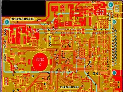
Our PCB reverse engineering service ensures high-quality product enhancement and cost savings. Benefit from our 100% success rate in PCB board copying, modification, schematic diagram derivation, BOM list creation, and PCB production. At SZOROD, we guarantee transparency and reliability. Try us for quick and accurate reverse engineering solutions.https://pcb-reverse-engineering.com/
28 posts
Don't wanna be here? Send us removal request.
Last Seen Blogs

gimmeheart
Heart Hunter The Arcana

rabbitremains
IM NOT A BUNY

kutonik
Personal Anime Blog

things-my-zr-playlist-did
Things my ZR playlist did

neonpurpleobject
purpul & neon
Text
The Art and Science of PCB Reverse Engineering: A Comprehensive Guide
In the world of electronics, understanding how a printed circuit board (PCB) works can be crucial for troubleshooting, innovation, and learning. PCB reverse engineering is a process that allows engineers, hobbyists, and researchers to dissect and comprehend the intricate designs of existing PCBs. Whether you're looking to replicate an old design, learn about advanced technologies, or modify existing hardware, PCB reverse engineering offers valuable insights and opportunities. In this blog post, we’ll explore the essentials of PCB reverse engineering, its benefits, and practical tips for getting started.
What is PCB Reverse Engineering?
PCB reverse engineering is the process of analyzing and deconstructing a PCB to understand its layout, design, and functionality. This typically involves examining the physical board and its components to recreate or modify the circuit’s schematic diagram and design files. The goal is to uncover the design details that are not readily available from the manufacturer, enabling you to replicate or improve the existing design.
Why Engage in PCB Reverse Engineering?
Learning and Education: For students and hobbyists, reverse engineering provides a hands-on way to learn about electronic circuit design, component functions, and board layout. It’s a practical method to understand how various components interact within a circuit.

Repair and Maintenance: When dealing with older or discontinued hardware, PCB reverse engineering can help in diagnosing faults and replacing faulty parts. This is particularly useful for repairing vintage electronics where original schematics are no longer available.
Innovation and Design: Engineers often use reverse engineering to analyze competitor products, understand their design choices, and find areas for improvement. By learning from existing designs, they can innovate and create better, more efficient products.
Legacy Support: Companies maintaining legacy systems may need to reverse engineer PCBs to continue providing support, upgrades, or replacements for outdated technology.
The PCB Reverse Engineering Process
Reverse engineering a PCB involves several steps, each requiring precision and careful analysis. Here’s a simplified overview of the process:
Disassemble the PCB
Carefully remove the PCB from its enclosure or casing. Use tools like tweezers and anti-static mats to handle the board and avoid damaging sensitive components.
Document the Board
Take high-resolution photographs of both the top and bottom layers of the PCB. These images will serve as reference material during the reverse engineering process. Ensure that the images are clear and well-lit.
Identify Components
Label and identify all components on the PCB. This includes resistors, capacitors, integrated circuits (ICs), and connectors. Use a multi meter or component tester to help identify and measure components if necessary.
Trace the Circuit
Use the photographs to trace the circuit connections. This involves mapping out the paths of electrical connections between components. Tools like PCB design software can assist in recreating the circuit schematic.
Create the Schematic Diagram
Based on your tracing, create a schematic diagram that represents the electrical design of the PCB. This step is crucial for understanding how the circuit functions and for making any modifications.
Design the PCB Layout
Once the schematic is complete, design a PCB layout that matches the original design. PCB design software can be used to create and refine the layout, ensuring that it accurately reflects the original board’s design.
Verify and Test
Before finalizing the design, verify that the recreated PCB functions as intended. Build a prototype and test it to ensure that it meets the required specifications and performs correctly.
PCB reverse engineering is a powerful technique for understanding and working with electronic circuits. Whether you’re aiming to repair vintage hardware, learn about circuit design, or innovate in the field of electronics, mastering the art of PCB reverse engineering can provide significant advantages. By following the steps outlined in this guide and utilizing the right tools, you can delve into the intricate world of PCB design and uncover the secrets behind your favorite electronic devices.
0 notes
Text
Clone PCB Service: A Comprehensive Solution for Reverse Engineering and Innovation
In the modern world of electronics and hardware development, Printed Circuit Boards (PCBs) are the backbone of most devices, ranging from simple gadgets to highly complex systems. However, there are times when engineers and businesses need to replicate or modify existing PCBs, either to improve upon a design, produce compatible hardware, or reverse-engineer devices. This is where Clone PCB service comes into play. This blog will explore the fundamentals of PCB cloning, its special benefits, and why this service is invaluable for innovation and reverse engineering.
What Is a Clone PCB Service?
PCB cloning requires advanced technical knowledge and tools to extract the necessary information from the original board, especially when the schematics or design files are unavailable. A professional clone PCB service can handle this process with precision, producing a board identical to the original, or one that has been enhanced to meet updated specifications.
Special Impressions of Clone PCB Services
1. Enabling Reverse Engineering for Legacy Devices
One of the primary uses of clone PCB services is reverse engineering legacy devices, especially when the original design files are no longer available. Many businesses still rely on older hardware, and when a PCB becomes obsolete, it can be difficult to find replacements. Clone PCB services allow businesses to recreate these essential components, ensuring they can continue to support and maintain their devices without completely overhauling their systems.
2. Improving Existing PCB Designs
Beyond simple duplication, clone PCB services offer a valuable opportunity for improvement. Sometimes the original design of a PCB is outdated or inefficient. Through cloning, engineers can optimize the design, enhance performance, reduce size, or add new functionality while keeping the core design intact. Clone PCB service allows businesses to make iterative improvements without starting from scratch.
3. Cost-Effective Production
For companies that need to produce multiple copies of a specific PCB, cloning can be a highly cost-effective solution. Once a PCB has been successfully cloned, it can be produced in bulk, saving on the costs of designing a new PCB from the ground up. Clone PCB services can significantly reduce development costs and time, especially when working with complex or proprietary technology.
4. Design Reuse and Customization
Clone PCB services allow companies to reuse a successful design for new applications. By duplicating an existing design and modifying it for new functionality, businesses can save development time and resources. This is particularly useful for companies that manufacture a range of similar products and want to leverage a tested design in multiple applications with slight modifications.
The Clone PCB service is an essential tool for reverse engineering, innovation, and cost-effective production in the electronics industry. It offers businesses the ability to replicate, improve, and customize existing PCB designs, enabling them to support legacy devices, optimize performance, and streamline their production processes. While intellectual property and ethical considerations must be respected, the benefits of PCB cloning far outweigh the challenges, making it a valuable service in today's fast-paced technological world.
0 notes
Text
Mastering PCB Reverse Engineering: A Comprehensive Guide
Circuit boards that have been printed (PCBs) are the foundation of modern electronics. They are everywhere, from your smartphone to your home appliances. PCB reverse engineering is a vital process that allows engineers and hobbyists to understand and replicate these crucial components. In this guide, we'll dive into PCB reverse engineering, exploring its significance, methods, and practical applications.
What is PCB Reverse Engineering?
Reverse engineering a printed circuit board is dissecting it to determine its layout and purpose. The goal is to recreate the board's schematics, layout, and connections. This process of pcb reverse engineering is crucial for repairing, improving, or replicating existing electronic devices. By examining how components are connected, engineers can troubleshoot issues or design compatible replacements.
Why is PCB Reverse Engineering Important?
PCB reverse engineering serves several purposes. It helps in:
Repairs and Maintenance: By understanding the layout and connections, technicians can fix malfunctioning devices.
Legacy Systems: Many older systems have outdated or unavailable documentation. Reverse engineering aids in the upkeep and modernization of these systems.
Security Analysis: It is used to identify vulnerabilities and improve the security of electronic systems.
Innovation: Engineers can learn from existing designs and develop improved versions or entirely new devices.
Methods of PCB Reverse Engineering
There are several methods of pcb reverse engineering. Here are the most common techniques:
1. Visual Inspection
The simplest method involves visually inspecting the PCB. Using a magnifying glass or microscope, you can examine the components and their connections. This method is often the first step in understanding the board's layout.

2. Circuit Tracing
Tracing a circuit entails navigating the PCB's electrical routes. By using tools like continuity testers or multimeters, you can map out the connections between different components. This technique is useful for creating a basic schematic of the circuit.
3. Decapsulation and Microscopy
For detailed analysis, especially in the case of integrated circuits (ICs), decapsulation and microscopy are used. An IC's covering layers must be removed during decapsulation in order to access its interior circuitry. Then, you can use microscopy to look at the circuit's minute features.
4. Software Tools
Reverse engineering can be substantially improved by using contemporary software technologies. Programs like KiCad and Eagle allow you to create digital schematics and layouts from your findings. These tools can also simulate the circuit to ensure accuracy.
Practical Applications of PCB Reverse Engineering
Reverse engineering of PCBs has several applications:
Product Development: Companies use reverse engineering to improve or modify existing products.
Educational Purposes: It helps students and hobbyists understand complex electronic systems.
Competitive Analysis: Businesses analyze competitors' products to understand their design and functionality.
PCB reverse engineering is a powerful technique that opens up numerous possibilities in electronics. Whether you're repairing an old device, analyzing security vulnerabilities, or innovating new technology, understanding how PCBs work is crucial. By mastering pcb reverse engineering, you can unlock the secrets of electronic designs and drive advancements in technology. For anyone involved in electronics, PCB reverse engineering is an invaluable skill. Embrace it to enhance your understanding, solve complex problems, and push the boundaries of what's possible.
0 notes
Text
Understanding IC Crack: What It Is and How to Prevent It
IC crack is a term that refers to the physical damage and malfunctioning of integrated circuits (ICs) due to cracks in their packaging. These tiny but vital components are at the heart of today's electronics, appearing in everything from cellphones to automobiles. An IC crack can lead to serious performance issues, including system failures and reduced reliability.
Causes of IC Crack
Several factors contribute to IC crack. One primary cause is thermal stress. Integrated circuits often experience significant temperature fluctuations, especially in high-performance environments. These temperature changes can cause the materials in the IC to expand and contract, eventually leading to cracks.
Another cause is mechanical stress. During manufacturing or handling, ICs can be subjected to physical forces. These stresses can damage the IC's structure if not properly managed. Inadequate soldering techniques during assembly can also contribute to the problem, making IC crack a common issue in poorly manufactured electronic devices.
Impact of IC Crack
The effects of an IC crack are far-reaching. When an IC crack occurs, it can disrupt the flow of electrical signals within the circuit. This disruption often results in erratic device behavior, reduced performance, and in severe cases, complete system failure. The impact is not limited to performance alone; it can also lead to safety issues, especially in critical systems such as medical devices and automotive electronics.
Preventing IC Crack
Preventing IC crack involves several strategies, primarily focusing on managing thermal and mechanical stresses. Here are some practical tips:

Use Quality Materials: Ensure that high-quality materials are used in the manufacturing and packaging of ICs. This lowers the possibility of material fatigue and cracking.
Optimize Thermal Management: Implement effective cooling systems to manage the heat generated by ICs. Good thermal management helps minimize the expansion and contraction of materials.
Improve Handling Procedures: Train personnel in proper handling techniques to avoid mechanical stress during manufacturing and assembly. To decrease the danger of physical injury, use the proper tools and practices.
Adopt Robust Soldering Techniques: Utilize advanced soldering techniques and equipment to ensure reliable connections between ICs and other components. Poor soldering might increase the chance of cracking.
IC crack is a major issue that can undermine the accuracy and efficiency of electronic equipment. By understanding its causes and implementing preventive measures, manufacturers and users can significantly reduce the risk of IC crack. Emphasizing quality materials, effective thermal management, and proper handling techniques are essential steps in ensuring the longevity and functionality of integrated circuits. In the ever-evolving world of electronics, staying informed about issues like IC crack and adopting best practices can make a significant difference in device performance and reliability. Remember, addressing these small but critical problems can lead to substantial improvements in your electronic systems. For more insights into electronic component issues and solutions, stay tuned to our blog. We provide qualified guidance and updates to help you remain current and ahead of the curve.
0 notes
Text

Get Excellent PCB REVERSE ENGINEERING SERVICES by SZOROD
Discover the excellency of reverse engineering with SZOROD. With experience spanning over 20 years, we provide a comprehensive suite of PCB reverse engineering services. FromPCB copying to modification and intricate chip unlocking solutions, we ensure 100% success. All our services come with a guarantee of accuracy and reliability. Get a 100%-quality solution with transparent pricing and round-the-clock availability. Trust us for reliable services.https://pcb-reverse-engineering.com/
0 notes
Text
Unlocking Innovation: PCB Reverse Engineering Services
PCB reverse engineering services are essential for understanding and replicating existing printed circuit boards (PCBs). In order to extract the design of a physical PCB, including its layout, component list, and schematic diagrams, this technique entails disassembling the board. This service is crucial for various applications, from repairing and refurbishing old devices to developing new products based on proven designs.
Why Opt for PCB Reverse Engineering Services?
In today’s rapidly evolving technology landscape, pcb reverse engineering services offer several advantages. First, they enable businesses to reproduce outdated or obsolete PCBs when original designs or manufacturing files are no longer available. This can be particularly valuable for maintaining and repairing legacy systems.
Second, PCB reverse engineering helps in creating compatible replacements for custom or proprietary circuits. By understanding the intricate details of a PCB, engineers can develop new versions that are functionally identical to the original. This ensures continuity in product performance and compatibility with existing systems.
How Does the PCB Reverse Engineering Process Work?
The process begins with acquiring a physical PCB. The board is meticulously examined and documented using high-resolution imaging techniques. Components are then removed, and each layer of the PCB is scanned and analyzed. This step is critical for capturing the detailed layout and connections of the circuit.
After obtaining the scans, skilled technicians use advanced software to recreate the PCB’s schematic diagrams and layout files. These digital files are compared with the original board to ensure accuracy and completeness. This comprehensive approach guarantees that the reverse-engineered PCB matches the original’s functionality and performance.
The Advantages of Expert Services for PCB Reverse Engineering
Opting for professional pcb reverse engineering services provides several key benefits. It guarantees exceptional quality and precision in the PCB reproduction, to start with. Professionals use state-of-the-art equipment and techniques to achieve precise results, which is crucial for maintaining the integrity of the original design.
Professional services can also facilitate the creation of new products by streamlining the development process. Businesses can cut expenses and development time while guaranteeing that their new products are based on dependable and tested technology by utilizing pre-existing PCB designs.
Industries That Benefit from PCB Reverse Engineering
Services for PCB reverse engineering are used in many different sectors. In the medical field, for instance, they help in refurbishing and maintaining complex diagnostic and monitoring equipment. In the industrial sector, reverse engineering is used to replicate control boards for machinery and automation systems.
The consumer electronics sector also benefits from these services, as they enable the repair and upgrade of devices like smartphones and gaming consoles. Furthermore, PCB reverse engineering is essential to the automotive industry's upkeep and advancement of electronic control units and sensors.
Why Choose Our PCB Reverse Engineering Services?
Our pcb reverse engineering services stand out due to our extensive experience and commitment to quality. We employ a detailed and precise approach to ensure that every PCB we reverse engineer meets the highest standards. Our team uses advanced technology to deliver accurate and reliable results, helping you achieve your project goals efficiently.
0 notes
Text
A Complete Guide to Understanding the IC Cracking Process
In the world of electronics and technology, the term crack IC refers to a specialized process that involves accessing and deciphering the encrypted data within integrated circuits (ICs). This is a critical skill for various applications, from repairing old equipment to advanced research and development. In this blog, we will explore what it means to crack IC, why it is necessary, and the methods used to achieve it.
What Does It Mean to Crack an IC?
To crack IC means to gain access to the data stored in an IC that is protected by encryption or other security measures. Integrated circuits are found in nearly every electronic device, from household appliances to complex industrial machinery. They often contain valuable programming and data that might be inaccessible due to encryption or obfuscation.
Cracking ICs can involve either retrieving lost data, understanding how a particular chip functions, or even reverse engineering to improve or replicate technology. The need to crack IC arises in several scenarios, including when dealing with discontinued products, recovering data from failed chips, or analyzing competitive technology.
Why Is Cracking IC Necessary?
Here are some common reasons why you might need to crack IC:
Repairing Discontinued Products: Older devices with ICs that are no longer produced can be repaired by accessing the data within the chips. Cracking ICs can provide the necessary information to fix or replace components.
Data Recovery: In cases where important data is lost or corrupted, cracking IC can help recover the information stored within the chip.
Reverse Engineering: For engineers and researchers, cracking IC allows for detailed analysis of how a chip works. This can lead to improved designs or new innovations.
Understanding Competitor Technology: If you are working in a competitive field, crack IC can help you understand and potentially improve upon the technology used by others.
Methods to Crack ICs
Hardware-Based Cracking: This method involves physically accessing the IC to retrieve data. Techniques such as decapsulation, where the chip is carefully opened, and the use of focused ion beams (FIB) to analyze the internal circuits are common.
Software-Based Cracking: Known as non-intrusive attacks, this approach uses software tools to bypass encryption without physically damaging the chip. Techniques include voltage and current attacks, as well as using specialized software to extract data. This method is less invasive and preserves the integrity of the IC but can be more complex and less reliable depending on the chip’s encryption.
Choosing the Right Service for Cracking ICs
When searching for IC-cracking services, take into account the following aspects:
Experience: Choose a provider with a proven track record in cracking ICs. Experience in handling various chip models and encryption methods is crucial for success.
Technology: Ensure the service uses advanced tools and techniques for both hardware and software-based cracking. This ensures accuracy and effectiveness.
Reputation: To ascertain the reliability and quality of the service that the business provides, look for previous evaluations and comments from clients.
Legal Compliance: Confirm that the crack IC services comply with legal regulations to avoid any potential issues.
Understanding how to crack ICs is essential for many professionals working with technology. Whether you need to repair outdated equipment, recover lost data, or conduct research, knowing how to access and interpret the data within an IC can be highly beneficial. By choosing the right techniques and working with experienced professionals, you can successfully navigate the complexities of cracking ICs and achieve your technical goals.
0 notes
Text
Understanding Clone PCB Service: A Comprehensive Guide
For those looking to replicate or repair printed circuit boards (PCBs), a clone PCB service offers a valuable solution. This service allows you to duplicate existing PCBs with high accuracy, ensuring that your electronic devices function as intended. Here’s everything you need to know about clone PCB service and how it can benefit your projects.
What is Clone PCB Service?
A clone PCB service involves the replication of existing PCBs, capturing their design and functionality with exact precision. This service is often used for duplicating old, discontinued boards or for creating prototypes based on existing designs. The process typically includes creating a detailed copy of the PCB layout, components, and connections, ensuring that the new board operates exactly like the original.

Benefits of Using Clone PCB Service
1. Cost-Effective Solution
Opting for a clone PCB service can be more cost-effective than designing a new PCB from scratch. By replicating an existing board, you save on design and development costs, making it an economical choice for both personal and professional projects.
2. Time Efficiency
Designing a PCB can be time-consuming. A clone PCB service accelerates the process by providing a ready-made solution. This is particularly beneficial when you need to replicate a working design quickly for production or repair purposes.
3. Preservation of Legacy Designs
For those working with older technology, a clone PCB service helps preserve legacy designs. If a PCB is no longer in production or is difficult to source, cloning allows you to continue using and maintaining older equipment without compromising on performance.
4. Enhanced Accuracy
Modern clone PCB services use advanced technology to ensure high accuracy in replication. This means that the cloned PCB will match the original’s specifications precisely, reducing the risk of errors and ensuring consistent performance.
How Clone PCB Service Works
1. Design Analysis
Analyzing the original PCB design is the first stage in a clone PCB service. This involves examining the layout, traces, components, and connections. High-resolution imaging and scanning technologies are often used to capture detailed information.
2. Creating the Clone
Once the design is analyzed, the cloning process begins. This includes replicating the PCB layout and transferring it onto a new board. The process may involve both manual and automated techniques to ensure precision.
3. Testing and Validation
After the clone is created, it undergoes rigorous testing to ensure it functions exactly like the original PCB. This step is crucial for verifying that the cloned board meets all performance and reliability standards.
Choosing the Right Clone PCB Service
When selecting a clone PCB service, consider the following factors:
Experience and Reputation: Select a service provider who has a solid track record and satisfied clients.
Technology and Equipment: Ensure the provider uses up-to-date technology and equipment for accurate cloning.
Turnaround Time: Check the service provider’s turnaround time to ensure it aligns with your project deadlines.
Cost: Examine prices to identify a service that provides a decent trade-off between price and quality.
A clone PCB service is an essential resource for those needing to replicate or repair printed circuit boards. By providing cost-effective, accurate, and timely solutions, this service supports both personal and professional electronics projects. Whether you’re preserving legacy designs or accelerating prototyping, choosing the right clone PCB service ensures your PCBs function flawlessly and meet your project requirements.
0 notes
Text
Understanding PCB Copy Services: A Deep Dive into the World of Copy PCB
PCB copying is a vital service in the electronics industry, offering a range of benefits from cost-effective manufacturing to intellectual property recovery. SZORODis a trusted partner for companies looking for PCB copy services, offering advanced techniques, customized solutions, and a commitment to quality. With their expertise and dedication, SZORODensures that every copied PCB is a perfect match to the original, helping businesses maintain continuity and drive innovation in their products.
0 notes
Text
Expert Services to Crack ICs with SZOROD
SZOROD is your go-to expert for all IC decryption needs. We specialize in unlocking encrypted chips to recover essential data or repair obsolete technology. With our advanced tools and over 20 years of experience, we ensure successful crack IC solutions while preserving the chip’s integrity. Our service is reliable, legal, and offers no charge for decryption failures. Whether it’s for outdated equipment or advanced research, SZOROD provides timely and effective results. Contact us today for professional IC unlocking services and get your solutions with confidence.
https://pcb-reverse-engineering.com/services/unlock-ic/
0 notes
Text
Unlock Your IC with Precision and Expertise from SZOROD
Discover expert IC crack services at SZOROD for high-difficulty and complex multi-layer PCB boards. We specialize in unlocking encrypted chips to recover valuable data or repair discontinued products. Our team uses advanced hardware and software techniques to ensure successful decryption while preserving the integrity of your ICs. With over 20 years of experience, SZOROD offers reliable and legal IC crack solutions with no charge for decryption failures. Whether you need assistance with outdated technology or specialized research, our professional service guarantees timely and effective results. Contact SZOROD today for a consultation and let us help you unlock your IC with confidence.
https://pcb-reverse-engineering.com/services/unlock-ic/
0 notes
Text
Unveiling Innovation: Exploring PCB Reverse Engineering
Within the domain of hardware and innovation, PCBs (Printed Circuit Sheets) serve as the spine of endless gadgets, from smartphones to mechanical apparatus. These perplexing sheets house layers of components and circuitry that empower gadgets to operate seamlessly. Be that as it may, what happens when we have to be get it, imitate, or move forward upon the plan of these PCBs? Usually where PCB invert building steps in—a intriguing prepare that opens the privileged insights inserted inside these crucial electronic components.
What is PCB reversing?
PCB invert designing includes dismembering and dissecting the structure, format, and usefulness of a printed circuit board to reveal its design details. This prepare is fundamental for different reasons, counting:
Understanding Bequest Plans:
As innovation advances, more seasoned PCB plans may have to be caught on or overhauled. PCB Reverse Engineering permits engineers to comprehend and record the usefulness of bequest PCBs that need comprehensive documentation.
Repair and Support:
When a gadget breakdowns and substitution parts are inaccessible or exorbitant, switch designing the PCB can offer assistance in repairing the gadget by recognizing flawed components or circuitry.
Change and Advancement:
Engineers can utilize turn around building to enhance existing plans or create unused cycles of PCBs with made strides execution, productivity, or usefulness.

Security Reviews:
Switch building is additionally utilized to survey the security vulnerabilities of PCBs, ensuring they meet rigid cyber security standards.
The Method of PCB Switch Building
The method of invert designing a PCB ordinarily includes a few key steps:
Physical Investigation:
This step includes carefully looking at the PCB's physical traits, such as its measure, shape, and component arrangement. Devices such as amplification gadgets, callipers, and X-ray imaging may be utilized to uncover covered up layers or associations.
Electrical Investigation:
Engineers at that point conduct electrical tests to outline out the associations and functionality of the PCB. This may incorporate utilizing multi meters, oscilloscopes, or specialized testing gear to follow flag ways and degree voltage levels.
Schematic Capture:
Once the physical and electrical characteristics are caught on, engineers make a schematic chart that speaks to the PCB's circuitry and component associations. Program instruments like Hawk, Altium Originator, or OrCAD are commonly utilized for this reason.
Component Distinguishing proof:
Recognizing and archiving each component on the PCB is significant. This includes decoding portion numbers, producer points of interest, and details to guarantee exact replication or substitution.
Recreation:
Utilizing the schematic diagram and component information, engineers can reproduce the PCB plan. This may include creating a new format that mirrors the original or integrates improvements based on the analysis.
By unraveling the inward workings of printed circuit sheets, engineers can pick up bits of knowledge that drive advancements, cultivate development, and guarantee the longevity of electronic gadgets. PCB reverse engineering plays a pivotal part in innovation advancement and support. As innovation proceeds to advance, the hone of PCB invert building will stay instrumental in pushing the boundaries of what is conceivable in gadgets plan and usefulness.
0 notes
Text
Understanding the Process and Benefits of Clone PCB
A clone PCB refers to a printed circuit board that replicates the design of an existing board. This concept can be crucial for a variety of applications, including reverse engineering, prototype development, and even product duplication. In this article, we'll delve into what it means to clone a PCB, the process involved, and the benefits it can bring.
What is a Clone PCB?
In essence, a Clone PCB is a duplicate of an authentic printed circuit board (PCB). This copying process can be used for several reasons, such as creating a backup of a critical component, manufacturing a similar product, or conducting repairs on outdated electronics . Cloning a PCB involves duplicating its design and functionality while maintaining the same electrical characteristics and performance as the original board.
The Process of Cloning a PCB
Cloning a PCB involves several key steps to ensure that the final product matches the original board's specifications. This is a condensed explanation of the procedure:
Design Analysis : The first step in creating a clone PCB is to thoroughly analyze the design of the original board. Examining the design, component positioning, and electrical connection routing are all part of this. Advanced tools like scanning software and schematic capture programs can be used to capture and replicate these details accurately.

Reverse Engineering : After design analysis, the next phase is reverse engineering. This involves creating a detailed schematic and layout based on the analysis of the original PCB. Reverse engineering tools can help convert physical PCB designs into digital formats, making it easier to replicate the board.
Fabrication and Assembly : With the digital design files ready, the clone PCB can be fabricated. This involves printing the PCB design onto a substrate, etching away excess material, and then placing and soldering components onto the board. Quality control is crucial during this phase to ensure that the cloned board meets the original specifications.
Testing and Validation : Once the Clone PCB is assembled, it undergoes rigorous testing to verify that it functions as intended. This includes checking electrical performance, signal integrity, and overall reliability. The goal is to ensure that the cloned PCB performs identically to the original board in every aspect.
Benefits of Cloning a PCB
Cost-Effective Solutions : One of the primary benefits of a clone PCB is cost savings. Cloning can be a more affordable option compared to designing a new PCB from scratch, especially when replicating an existing, proven design.
Prototyping and Testing: For engineers and developers, cloning a PCB allows for rapid prototyping and testing. This can be especially useful for developing new products or testing modifications without the need for extensive redesign efforts.
Replacement for Obsolete Components: As technology evolves, certain PCBs and their components may become obsolete. Cloning a PCB provides a viable solution for replacing or repairing outdated electronics, ensuring continued functionality of critical systems.
Educational Purposes: Cloning PCBs can also serve educational purposes. It offers students and enthusiasts the opportunity to learn about PCB design and assembly by working with real-world examples.
Product Duplication: For manufacturers, cloning a PCB allows for the duplication of successful products. This can be beneficial for scaling production or creating variations of a popular design.
The process of creating a clone PCB involves a detailed and meticulous approach to ensure accuracy and functionality. By understanding and utilizing the cloning process, businesses and individuals can enjoy the benefits of cost-effective solutions, enhanced prototyping, and the ability to maintain and repair obsolete electronics. Whether for educational purposes, product duplication, or practical applications, cloning a PCB provides valuable opportunities in the world of electronics.
0 notes
Text
How to unlock GD32 chip IC?
TW earphone charging case, earphones and hearing aids, portable medical equipment, nursing detectors, low battery applications, three-phase BLDC and PMSM motors, electric tools, robots and remote control toys, industrial automation, wireless infrastructure, communication network cards, industrial applications, safety equipment, lithium battery charging and analog front-end monitoring, sweeping robots, aircraft model four axis aircraft, energy storage, etc.
https://pcb-reverse-engineering.com/news/gd32-unlock/
0 notes
Text
Demystifying PCB Cloning: Creating Copies of Printed Circuit Boards
The world of electronics thrives on innovation, but there are times when a proven design needs replication. This is where PCB cloning comes in. PCB, or Printed Circuit Board, cloning is the process of creating an exact replica of an existing circuit board. It's essentially reverse engineering a physical board to obtain its design files and recreate it.
Why Clone a PCB?
There are several reasons why someone might choose PCB cloning:
Replacement Parts: If a crucial piece of equipment relies on a discontinued PCB, cloning allows for the creation of replacements, ensuring the equipment's continued functionality.
Product Development: Cloning can be a time and cost-effective way to analyze existing designs and develop improved versions. By studying the layout and components, engineers can gain valuable insights for their own projects.
Rapid Prototyping: PCB clone can fast-track the prototyping stage for new products. With the core design already established, engineers can focus on modifications and testing.
Education and Learning: For hobbyists and electronics students, PCB cloning offers a practical way to understand circuit board design and functionality. By analyzing the physical board and recreating the schematics, they gain valuable hands-on experience.
The PCB Cloning Process
PCB cloning typically involves several steps:
· Physical Examination: The first step involves thoroughly examining the original PCB. This includes identifying the components used, their placement, and the routing of the traces that connect them.
· Component Identification: Each component on the board needs to be identified by its specific part number. This allows for sourcing the exact components or suitable alternatives during the cloning process.
· Reverse Engineering the Layout: The most intricate step involves extracting the design information from the physical board. This often involves high-resolution scanning and specialized software to recreate the trace layout and layer structure.
· Generating Design Files: The extracted design information is then used to generate Gerber files, which are the industry-standard format for PCB manufacturing. These files precisely define the layout of each layer in the PCB.
· Fabrication and Assembly: With the Gerber files in hand, the PCB clone can be fabricated by a PCB manufacturer. Finally, the components are soldered onto the newly created board, replicating the functionality of the original.
Legality of PCB Cloning
It's important to remember that PCB cloning is legal only if you have the right to modify and reproduce the original board. If you purchased a device and the PCB is part of it, then you generally have the right to clone it for personal use or repair purposes. However, PCB clone for commercial purposes without the proper licensing or permission from the original designer is a violation of intellectual property rights.
The Future of PCB Cloning
As technology advances, PCB cloning is becoming a more accessible and efficient process. Advancements in scanning technology and software tools are making it easier to extract design information from complex boards. Additionally, the growing availability of online PCB cloning services allows individuals and businesses to clone boards without the need for in-house expertise.
1 note
·
View note
Text
Breathing New Life into Electronics: PCB Reverse Engineering for PCB Cloning at SZOROD
Imagine finding a vintage device with unique functionality or a discontinued gadget with a sentimental value. Unfortunately, these treasures often suffer from outdated components or lack readily available replacements. This is where SZOROD's expertise in PCB Reverse Engineering comes in, offering the potential to create a PCB clone and breathe new life into these electronic gems.
PCB Reverse Engineering is the meticulous process of analyzing an existing Printed Circuit Board (PCB) to understand its design, functionality, and component interactions. By deconstructing the PCB, valuable insights can be gained, paving the way for various applications. One such application is PCB cloning, where a functional replica of the original PCB is created.

So, how does PCB Reverse Engineering lead to PCB cloning? Here's a simplified breakdown of the process:
Physical Examination: The PCB undergoes a thorough examination to identify all its components, including the ICs (Integrated Circuits) and passive components like resistors and capacitors.
Schematics and Layout Extraction: Using specialized techniques like layer imaging and etching, engineers meticulously map the connections between components, essentially creating a blueprint – the schematic diagram.
Component Analysis & Bill of Materials (BOM) Creation: Each component is analyzed to determine its specifications and a Bill of Materials (BOM) is compiled, listing all the necessary components to replicate the PCB.
Here's where the challenge arises. Sometimes, specific components, particularly complex ICs, might be obsolete or have proprietary designs. In these cases, SZOROD's engineering expertise comes into play. They can leverage alternative components with similar characteristics or even develop workarounds to achieve the desired functionality. This is where PCB Reverse Engineering goes beyond simple replication, potentially leading to improved or updated versions of the original design – a benefit not achievable with a straight-up PCB clone.

Once the BOM is finalized and any component sourcing hurdles are addressed, SZOROD's advanced PCB manufacturing capabilities come into play. They can fabricate the PCB clone using high-quality materials and cutting-edge production techniques, ensuring the new board functions reliably and matches the original design.
The applications of PCB Reverse Engineering and PCB cloning are vast. It allows SZOROD to:
Resurrect Discontinued Devices: By creating PCB clones, SZOROD can offer replacement PCBs for devices no longer in production, ensuring vintage equipment and cherished gadgets can be enjoyed for years to come.
Improve Upon Existing Designs: The process of PCB Reverse Engineering unveils the inner workings of a PCB. This knowledge can be used to identify areas for improvement, leading to PCB clones with enhanced features or better performance.
Develop Compatible Components: Through PCB Reverse Engineering, SZOROD can gain insights into the functionalities of proprietary ICs. This knowledge can then be used to develop compatible components, filling the gap for discontinued parts and keeping older devices operational.
In conclusion, PCB Reverse Engineering, with its potential for PCB cloning, is a powerful tool in SZOROD's arsenal. It allows them to breathe new life into old electronics, fostering innovation and ensuring that cherished technologies don't become relics of the past.
1 note
·
View note
Text
Understanding PCB Reverse Engineering Cost: Key Considerations and Special Facilities
PCB reverse engineering, a process that involves deconstructing a printed circuit board (PCB) to understand its design and functionality, is crucial in various industries. Whether it's for repairing outdated equipment, analyzing competitor products, or optimizing existing designs, PCB reverse engineering is an invaluable service. However, one of the main concerns for businesses and individuals is the cost associated with this process. In this article, we will explore the factors influencing PCB reverse engineering costs and the special facilities that make this service possible.
Factors Influencing PCB Reverse Engineering Cost:
Complexity of the PCB Design
The complexity of a PCB reverse engineering cost significantly impacts the reverse engineering cost. A simple single-layer board with a few components will be less expensive to reverse engineer compared to a multi-layer board with numerous components. The intricacy of the circuitry, the density of the components, and the type of components used all contribute to the overall cost.
Number of Layers
PCBs can range from single-layer to multi-layer designs. Multi-layer boards require more time and expertise to reverse engineer, as each layer must be meticulously analyzed and documented. The more layers a PCB has, the higher the cost of reverse engineering.
Type of Components
The type of components used in the PCB also affects the cost. Surface mount devices (SMDs) are generally more challenging to reverse engineer than through-hole components due to their smaller size and higher density.
Documentation and Testing Requirements
The extent of documentation and testing required can also impact the cost. Comprehensive documentation, including detailed schematics, bill of materials (BOM), and layout files, is essential for successful reverse engineering. Additionally, thorough testing to ensure the PCB reverse engineering cost functions correctly.
Advanced Scanning and Imaging Equipment
State-of-the-art scanning and imaging equipment are essential for accurate PCB reverse engineering. High-resolution scanners and X-ray machines allow engineers to visualize and analyze the intricate details of a PCB without physically dismantling it.
Experienced Engineers and Technicians
Skilled engineers and technicians with extensive experience in PCB design and reverse engineering are vital for successful projects. Their expertise ensures accurate interpretation of scanned data, identification of components, and creation of precise documentation. Their knowledge of various PCB technologies and industry standards also contributes to the quality and reliability of the reverse-engineered board.
Testing and Validation Laboratories
Dedicated testing and validation laboratories equipped with the latest testing equipment are essential for ensuring the functionality and reliability of reverse-engineered PCBs. These facilities conduct rigorous testing, including electrical, thermal, and environmental tests, to verify that the reverse-engineered board meets the required specifications and performs as expected in real-world conditions.
The PCB reverse engineering cost is influenced by various factors, including the complexity of the design, the number of layers, the type of components, and the documentation and testing requirements. Special facilities, such as advanced scanning and imaging equipment, CAD software and tools, experienced engineers and technicians, and dedicated testing laboratories, play a crucial role in the reverse engineering process.
0 notes