#Chip components and Electronic parts printing process manufacturing.
Text
Enhancing SMT Efficiency with Panasonic Feeders

In the fast-paced world of electronics manufacturing, precision, and speed are key to staying competitive. Panasonic feeders are critical components in surface-mount technology (SMT) equipment, designed to improve the efficiency and accuracy of automated PCB assembly processes. These feeders ensure that electronic components are delivered seamlessly to pick-and-place machines, which are responsible for placing tiny components onto printed circuit boards (PCBs).
What is a Panasonic Feeder? A Panasonic feeder is a device used in SMT production lines to feed components, such as resistors, capacitors, and ICs, to the placement head of a pick-and-place machine. These feeders handle components housed in various packaging formats like tapes, trays, or tubes and ensure that each component is accurately aligned for placement. Panasonic feeders are known for their reliability, precision, and adaptability to different component types and sizes.
Key Features and Benefits:
High Precision: Panasonic feeders are engineered for high accuracy in component delivery. This precision ensures that each component is placed correctly on the PCB, reducing the risk of assembly errors and improving product quality.
Versatility: Whether dealing with small chip components or larger, more complex parts, Panasonic feeders can accommodate a wide range of component sizes, making them versatile for various manufacturing needs.
Efficiency: By automating the component-feeding process, Panasonic feeders help to speed up production lines, reducing assembly time and increasing throughput. This allows manufacturers to meet high-volume demands more efficiently.
Applications: Panasonic feeders are widely used in industries such as consumer electronics, automotive electronics, and telecommunications. Their reliability and precision make them essential for manufacturers aiming to produce high-quality products at a fast pace.
Conclusion: Panasonic feeders are crucial components in the SMT manufacturing process, offering precision, speed, and flexibility. By optimizing the delivery of components to pick-and-place machines, these feeders help manufacturers enhance their production efficiency and maintain high standards of product quality.
0 notes
Text
Exactly to Try to find in a Trustworthy PCB Manufacturer and Supplier in China?

When it pertains to locating a reputable PCB supplier and provider in China, you're certainly not just appearing for anybody - you're seeming for a partner that may aid your business prosper. But with numerous alternatives on call, it could be frustrating to recognize where to begin. You'll would like to consider a maker's experience and certifications, including ISO 9001, however that is actually only the starting point. What else should you be trying to find, and just how can you guarantee that your chosen provider has the capabilities and proficiency to satisfy your distinct necessities? That is actually an inquiry you'll desire to explore additionally.
Experience and Certifications
With over a many years of experience in the PCB production market, a trusted Mandarin PCB manufacturer has developed on its own as a counted on companion for business worldwide. You are actually searching for a pcb board supplier that possesses an effective keep track of record in delivering top notch products punctually. A trusted pcb board supplier in China need to have significant experience in manufacturing different sorts of PCBs, consisting of ceramic pcb and dual sided pcb. When examining a pcb board china supplier, you ought to examine their certifications. Appear for qualifications like ISO 9001, ISO 14001, and IATF 16949, which demonstrate the producer's devotion to quality, environmental protection, and automobile quality monitoring. Are you prepared to elevate your electronic devices job along with high-quality elements? Contact PCB board today to start on your customized solutions.
Quality Assurance Procedures
A robust quality assurance system is elemental to a reputable Mandarin PCB supplier's procedures. When examining a possible provider, you need to seek a quality assurance system that encompasses the whole entire pcb board production method, from basic material evaluation to end product screening. A trusted dual sided pcb manufacturer need to possess a quality command group that assesses every stage of the production method, featuring PCB assembly, part procurement, and installation. When it comes to hitech pcb board manufacturing, quality command solutions must consist of rigorous examination process for complicated elements, like silicon chips and ports. A printed motherboard manufacturer should likewise possess a system in position for tracking and controlling procedure variations, such as temperature level and moisture.
Development Functionalities
Various production innovations and advanced tools allow a dependable Mandarin PCB manufacturer to produce premium panels properly. When assessing a possible provider, you'll wish to assess their development capacities to guarantee they can easily fulfill your requirements. Look for manufacturers along with knowledge in making sophisticated PCBs, such as hitech PCBs and hitech ceramic pcb panels. These sorts of panels often call for specific tools and methods. Likewise, think about makers that give a stable of PCB kinds, featuring light weight aluminum PCBs. As an aluminum pcb distributor, they need to be capable to give premium boards with outstanding thermal energy. Double edge PCBs, which possess conductive coatings on each sides, likewise need specific production capabilities. Guarantee the maker has experience with these kinds of boards and can easily generate all of them to your specs.
Interaction and Support

Assessing a Chinese PCB maker's manufacturing capabilities is actually just the 1st step in promising a smooth and prosperous partnership. When it concerns collaborating with a distributor, like Hitech Circuits Co., Limited, a trusted PCB producer, effective communication and help are vital. You must appear for a supplier that can easily supply clear and succinct updates on your order status, component sourcing, and production timelines. A respectable supplier, such as a hitech ceramic PCB distributor or hitech aluminum PCB supplier, ought to have a dedicated group for client assistance. They ought to be actually responsive to your inquiries and concerns, resolving all of them in a well-timed and qualified fashion.
Prices and Payment Phrases
When partnering with a Chinese PCB producer, pricing and payment phrases are actually critical variables to analyze, as they straight impact your project's finances and general cost-effectiveness. You'll would like to contrast quotes from different suppliers to ensure you're getting the most effective rate for your hitech light weight aluminum PCB or even hitech ceramic PCB. Make certain to inquire about any added prices, such as tooling charges or even freight fees, that might not be actually featured in the initial quote. It's also vital to comprehend the payment phrases. A reputable ceramic pcb supplier or aluminum pcb maker need to provide versatile payment alternatives, including wire transactions, visa or mastercard, or even PayPal. Distrust manufacturers that require full payment upfront, as this may be an indication of a con.
Verdict
As you browse the structure landscape of PCB makers in China, a dependable partner is actually the sign that overviews you by means of the hurricane. Look for a manufacturer with a proven performance history, accreditations that radiate like badges of tribute, and a quality assurance system that's closed. With the ideal mix of experience, capabilities, and support, your PCB needs will certainly reside in really good hands, and your venture will definitely be actually the masterpiece you imagined.
3F, Bldg B5, Zhimeihuizhi Industrial Park
FuYong, Bao'an Dist. Shenzhen, GuangDong, China
+86-755-29630063
0 notes
Text
PCB Manufacturing: A Comprehensive Exploration of Modern Assembly Services
In the electronics manufacturing sector, PCB (Printed Circuit Board) assembly services are indispensable. Numerous companies provide rapid prototyping and mid-volume production services tailored to the intricate demands of diverse industries. This article delves into the complexities of these services, highlighting the technological prowess and strategic advantages of opting for domestic assembly options.
Innovative Prototyping and Expedited Assembly Services
Organizations specializing in PCB assembly emphasize their capability to execute rapid turnaround projects, typically within 1 to 5 days. These offerings are designed to support even the most complex or specialized boards, accommodating projects of any scale. Additional services such as Bill of Materials (BOM) validation and preliminary Design for Manufacturability (DFM) analysis are frequently included at no extra charge, demonstrating a dedication to quality and customer satisfaction from the beginning of the manufacturing journey.
Advantages of Domestic Mid-Volume Production
For mid-volume production, domestic PCB assembly offers several benefits. It is particularly valuable when quick turnaround times are essential or when projects contain sensitive intellectual property. Utilizing domestic facilities is also beneficial when products are destined for governmental agencies, involve export-restricted information, or when volumes are too small to benefit economically from offshore production. This method ensures greater control over the manufacturing process, improved traceability, and enhanced client involvement.
Tailored PCB Assembly Services
Top manufacturers expand their service offerings beyond basic assembly to include comprehensive support services. These may encompass component sourcing, rework and repair services, functional testing, and X-ray inspections, as well as specialized treatments such as encapsulation, potting, and various coatings. These customized services ensure that every aspect of PCB assembly is efficiently handled, from initial prototyping through to the completion of the final order.
Gaining a Competitive Advantage in PCB Assembly
Manufacturers that lead in PCB assembly often present several competitive benefits:
Swift, 24-hour turnaround for quotes.
Custom software tools for BOM validation.
Detailed DFM feedback.
Flexible procurement options for either turnkey or consigned parts.
No minimum order quantity, supporting a variety of project scales.
Advanced assembly techniques, including microelectronics and flip chip technologies.
These manufacturers typically select strategic equipment and keep their client base limited, ensuring personalized service and meticulous attention to detail.
Ensuring Quality and Achieving Certifications
Quality assurance is a cornerstone in PCB assembly, critical for ensuring the reliability and performance of the final products. This sector employs a suite of sophisticated inspection and testing procedures that are essential for maintaining high quality standards. Techniques like Solder Paste Inspection (SPI) and Automated Optical Inspection (AOI) are employed to detect any potential defects early in the assembly process.
X-ray analysis is another pivotal technique used to examine the internal features of PCBs, ensuring that hidden joints and components are correctly placed and soldered. Additionally, a variety of functional testing methods are utilized to verify that each board performs according to its design specifications under different conditions. Adherence to these rigorous practices is essential for achieving certifications that testify to the reliability and quality of the products. These certifications are often required by clients in highly regulated industries, underscoring the necessity of stringent quality controls in PCB manufacturing.
The Evolving Landscape of PCB Manufacturing
The PCB manufacturing industry is constantly evolving, propelled by technological advancements and the growing need for precision and efficiency. As firms continue to innovate and broaden their service range, the importance of selecting a PCB assembly partner with extensive capabilities and a solid quality management system becomes increasingly evident.
For entities requiring professional PCB assembly services, it is recommended to collaborate with manufacturers that not only meet the technical requirements but also align with strategic business objectives. This alignment is essential for fostering long-term partnerships and succeeding in sophisticated electronics manufacturing endeavors.
In summary, PCB manufacturing includes a broad spectrum of services and capabilities. From rapid prototyping to specialized mid-volume production, the industry provides customized solutions to satisfy the varied needs of its customers. By utilizing cutting-edge technologies and focusing on quality and client service, leading PCB assemblers are ideally positioned to meet the dynamic requirements of contemporary electronic devices.
0 notes
Text
Automated X-ray Inspection (AXI) - Topscom Technology
Increasing product complexity and component miniaturization have driven the need for more consistent inspection processes and alternative test methods. Topscom has responded to this need in several ways, including the addition of Automated X-ray Inspection (AXI) to our capabilities. AXI is designed to find structural solder faults including solder opens, shorts, insufficient solder, excessive solder, missing electrical parts, and mis-aligned components. This includes non-visible joints such as area-array packages (BGA, CSP, Flip Chip), parts under RF shielding, and some connector styles. Defects are rapidly detected and repaired with almost no debug time. https://is.gd/K6iFAW
PCB SMT assembly, China printed circuit board assembly, China PCB factory, China PCB fabrication, China PCB manufacturing, China PCB board, China PCB manufacturer, China PCB service, China PCB prototype, China PCB supplier, China PCB, PCB China, China PCB online, PCB board, China PCB assembly, PCBA China, China PCB design, PCB assembly, China PCB quote, PCBA, contract manufacturing China, China contract manufacturing, contract manufacturing, China electronic assembly, China electronic manufacturing, electronics manufacturing, electronic board manufacturers, China OEM manufacturing, OEM manufacturing, China cable wire harness assembly
0 notes
Text
What is the difference between PCB and PCBA?

1. What is PCB?
Multilayer Circuit Board
PCB, or Printed Circuit Board, which can be referred to in Chinese as circuit board, circuit board, printed circuit board, etc., is a key component in electronics manufacturing.PCB is designed as a flat plate, usually made of insulating material, on which conductive lines and connection points are laid. The layout of these conductive lines and connection points is designed according to the needs of the electronic components.They support the electronic components and enable connections between them.
2. What does PCBA mean?
Circuit Board Soldering
PCBA, i.e. Printed Circuit Board Assembly, is usually also referred to as PCB Assembly in foreign countries.PCBA is the next step of PCB, which involves putting a blank PCB board through a series of processes, including SMT placement, DIP insertion, and testing, etc., to end up with a finished product. This finished product is no longer a blank board, but a circuit board with certain functions and various electronic components installed on it, such as resistors, capacitors, chips, and so on. In fact, the core part of almost all electronic products is composed of PCBA.
3. The difference between PCBA and PCB?
The most crucial point to understand the difference between PCBA and PCB is their status and function:
PCB is an empty board with no electronic components installed on the surface, only conductive lines and connection points.
PCBA is processed and assembled on the blank PCB, installed a variety of electronic components, forming a circuit board with a specific function.
The PCB provides the basis for the placement of electronic components, while the PCBA assembles these components together so that they can work together to realize electric
0 notes
Text
The Elements of Your PCBs: A Comprehensive Guide to 10 Most Popular Electronic Components
With the increasing demand for electronic gadgets, automation, and the Internet of Things (IoT), the electronic sector has tremendous growth potential. According to reports, by 2025, the worldwide electronic market will observe an exponential revenue growth of CAGR 8,92% till 2029, resulting in $712.30 billion.
The small components often constitute the foundation of everything the electrical gadgets we use daily, from life-saving medical equipment to cell phones. Navigating this small segment of electronic component sourcing, though, can be intimidating, given the thousands of available component sources.
This blog will go into the top 10 most important and regularly used electronic components, outlining their roles and how they work to create the magic inside your PCBs (Printed Circuit Boards).

Top 10 Essential Electronic Components for PCB Manufacturers
Out of numerous electronic components used in PCB manufacturing, here are the 10 essential components.
1. Resistors:
The backbone of every circuit, resistors regulate the current flow. It is recognised as “R” in the diagram. Picture them as small barriers that control the flow of electricity. The amount of current flowing through them is determined by their resistance value, measured in ohms (Ω). Selecting the correct one for your design among the many available options is essential, as they come in different sizes and power levels.
2. Capacitors:
A capacitor is essentially a small energy storage device. Capacitors (C) are measured in F (farad). They serve as a temporary power source for your circuit by storing electrical charge and reducing voltage fluctuations. Ceramic and electrolytic varieties exist, and each has advantages in certain contexts.
3. Diode:
The third type of electrical device is the diode, which allows current to flow in just one direction. They protect delicate components and make sure the current flows properly, like security guards. Diodes are versatile and can regulate voltage, route signals, and rectify alternating current (AC). In PCBs the most commonly used diode is Zener diode that offers various voltage stabilization options.
4. Transistors:
In the electronic industry, transistors are everywhere. These microscopic technological wonders are the building blocks of integrated circuits (ICs) and other intricate parts, used to control and can amplify the current. Its function is to amplify weak signals into electrical signals with larger amplitudes making it an essential component in PCB.
5. Crystals and Oscillators:
These are the beating heart of many electronics. Oscillators create a steady clock signal by applying a specific frequency to the vibrations of crystals. From regulating microprocessors to facilitating radio transmission, this timing signal is crucial for a multitude of tasks.
6. Light-Emitting Diodes (LEDs):
Incredibly flexible, LEDs aren't limited to glitzy gadgets. They are perfect for indicator lights, displays, and backlighting since they transform electrical energy into light. They have a long lifespan and consume very little power.
7. Integrated Circuits (ICs):
Integrated circuits (ICs), sometimes called chips, are considered the most important invention in the electronic field. They incorporate millions of transistors and other components on a single silicon chip to create complicated functionality. Integral circuits (ICs) are the central processing units (CPUs) and memory chips (MCUs) of contemporary electronics.
8. Electromechanical Components (Switches and Relays):
Components connect electrical and physical parts, known as electromechanical components (such as switches and relays). Relays enable high-power applications as electrically controlled switches, while switches allow you to manually control the current flow.
9. Connectors:
Connectors, the essential component of PCB construction, guarantee secure connections between various on-board components and any external devices you may be using. The correct connector, whether a basic header or a complicated socket, is critical for the operation and integrity of the signal.
10. Transformers:
An electrical device that alters the alternating current voltage. It has a magnetic iron core and two or more primary and secondary coils that wind around it. A transformer can maintain the electrical power balance while converting the input voltage into the needed output voltage using the electromagnetic induction principle. Power systems, electronic devices, communication networks, and manufacturing all use transformers heavily.
Choosing the Right Components for Your PCB
Now that you know what these BoM components are, you can choose them for your PCB design and BoM data creation with care, but there are a few things to keep in mind:
Function: The purpose of each part of your circuit must be defined.
Detailed Specifications: Read the technical specs and BoM data carefully, especially those dealing with voltage ratings and current constraints.
Fitment and Size: Get the dimensions and virtual footprint of your components right so they'll fit snugly on your printed circuit board design.
Availability and Cost: Consider how easy it is to get your hands on the parts you need through dependable electronic component sourcing and how much they will cost.
In summary:
Gaining familiarity with these ten electronic parts and component sourcing will put you in a strong position to succeed in the thrilling field of printed circuit board design and production. The success of a project depends on dependable component sourcing. To make sure your PCBs work perfectly, team up with a reliable provider with a large selection of high-quality components.
Click here to get the instant quotation.
Contact us at [email protected] or +1(818) 886 8900 if you have any more questions about our PCB service.
This Blog Originally Posted Here: The Elements of Your PCBs: A Comprehensive Guide to 10 Most Popular Electronic Components
0 notes
Text
Researchers demonstrate the first chip-based 3D printer
New Post has been published on https://thedigitalinsider.com/researchers-demonstrate-the-first-chip-based-3d-printer/
Researchers demonstrate the first chip-based 3D printer

Imagine a portable 3D printer you could hold in the palm of your hand. The tiny device could enable a user to rapidly create customized, low-cost objects on the go, like a fastener to repair a wobbly bicycle wheel or a component for a critical medical operation.
Researchers from MIT and the University of Texas at Austin took a major step toward making this idea a reality by demonstrating the first chip-based 3D printer. Their proof-of-concept device consists of a single, millimeter-scale photonic chip that emits reconfigurable beams of light into a well of resin that cures into a solid shape when light strikes it.
The prototype chip has no moving parts, instead relying on an array of tiny optical antennas to steer a beam of light. The beam projects up into a liquid resin that has been designed to rapidly cure when exposed to the beam’s wavelength of visible light.
By combining silicon photonics and photochemistry, the interdisciplinary research team was able to demonstrate a chip that can steer light beams to 3D print arbitrary two-dimensional patterns, including the letters M-I-T. Shapes can be fully formed in a matter of seconds.
In the long run, they envision a system where a photonic chip sits at the bottom of a well of resin and emits a 3D hologram of visible light, rapidly curing an entire object in a single step.
This type of portable 3D printer could have many applications, such as enabling clinicians to create tailor-made medical device components or allowing engineers to make rapid prototypes at a job site.
“This system is completely rethinking what a 3D printer is. It is no longer a big box sitting on a bench in a lab creating objects, but something that is handheld and portable. It is exciting to think about the new applications that could come out of this and how the field of 3D printing could change,” says senior author Jelena Notaros, the Robert J. Shillman Career Development Professor in Electrical Engineering and Computer Science (EECS), and a member of the Research Laboratory of Electronics.
Joining Notaros on the paper are Sabrina Corsetti, lead author and EECS graduate student; Milica Notaros PhD ’23; Tal Sneh, an EECS graduate student; Alex Safford, a recent graduate of the University of Texas at Austin; and Zak Page, an assistant professor in the Department of Chemical Engineering at UT Austin. The research appears today in Nature Light Science and Applications.
Printing with a chip
Experts in silicon photonics, the Notaros group previously developed integrated optical-phased-array systems that steer beams of light using a series of microscale antennas fabricated on a chip using semiconductor manufacturing processes. By speeding up or delaying the optical signal on either side of the antenna array, they can move the beam of emitted light in a certain direction.
Such systems are key for lidar sensors, which map their surroundings by emitting infrared light beams that bounce off nearby objects. Recently, the group has focused on systems that emit and steer visible light for augmented-reality applications.
They wondered if such a device could be used for a chip-based 3D printer.
At about the same time they started brainstorming, the Page Group at UT Austin demonstrated specialized resins that can be rapidly cured using wavelengths of visible light for the first time. This was the missing piece that pushed the chip-based 3D printer into reality.
“With photocurable resins, it is very hard to get them to cure all the way up at infrared wavelengths, which is where integrated optical-phased-array systems were operating in the past for lidar,” Corsetti says. “Here, we are meeting in the middle between standard photochemistry and silicon photonics by using visible-light-curable resins and visible-light-emitting chips to create this chip-based 3D printer. You have this merging of two technologies into a completely new idea.”
Their prototype consists of a single photonic chip containing an array of 160-nanometer-thick optical antennas. (A sheet of paper is about 100,000 nanometers thick.) The entire chip fits onto a U.S. quarter.
When powered by an off-chip laser, the antennas emit a steerable beam of visible light into the well of photocurable resin. The chip sits below a clear slide, like those used in microscopes, which contains a shallow indentation that holds the resin. The researchers use electrical signals to nonmechanically steer the light beam, causing the resin to solidify wherever the beam strikes it.
A collaborative approach
But effectively modulating visible-wavelength light, which involves modifying its amplitude and phase, is especially tricky. One common method requires heating the chip, but this is inefficient and takes a large amount of physical space.
Instead, the researchers used liquid crystal to fashion compact modulators they integrate onto the chip. The material’s unique optical properties enable the modulators to be extremely efficient and only about 20 microns in length.
A single waveguide on the chip holds the light from the off-chip laser. Running along the waveguide are tiny taps which tap off a little bit of light to each of the antennas.
The researchers actively tune the modulators using an electric field, which reorients the liquid crystal molecules in a certain direction. In this way, they can precisely control the amplitude and phase of light being routed to the antennas.
But forming and steering the beam is only half the battle. Interfacing with a novel photocurable resin was a completely different challenge.
The Page Group at UT Austin worked closely with the Notaros Group at MIT, carefully adjusting the chemical combinations and concentrations to zero-in on a formula that provided a long shelf-life and rapid curing.
In the end, the group used their prototype to 3D print arbitrary two-dimensional shapes within seconds.
Building off this prototype, they want to move toward developing a system like the one they originally conceptualized — a chip that emits a hologram of visible light in a resin well to enable volumetric 3D printing in only one step.
“To be able to do that, we need a completely new silicon-photonics chip design. We already laid out a lot of what that final system would look like in this paper. And, now, we are excited to continue working towards this ultimate demonstration,” Jelena Notaros says.
This work was funded, in part, by the U.S. National Science Foundation, the U.S. Defense Advanced Research Projects Agency, the Robert A. Welch Foundation, the MIT Rolf G. Locher Endowed Fellowship, and the MIT Frederick and Barbara Cronin Fellowship.
#000#3-D printing#3d#3D printing#amplitude#applications#box#Building#career#career development#challenge#change#chemical#Chemical engineering#Chip Design#chips#collaborative#computer#Computer Science#crystal#defense#Defense Advanced Research Projects Agency (DARPA)#Design#development#direction#electric field#Electrical Engineering&Computer Science (eecs)#Electronics#engineering#engineers
0 notes
Text
SMT production process

Program the SMT placement machine
According to the BOM position map provided by the customer, program the coordinates of the location of the components. Then carry out the first piece with the SMT chip processing data provided by the customer.
Printing solder paste
The solder paste is stenciled to the PCB board where the electronic component SMD needs to be soldered to prepare for the soldering of the components. The equipment used is a screen printing machine (printing machine), which is located at the forefront of the SMT chip processing production line.
SPI
Solder paste detector, detects whether the solder paste printing is a good product, whether there is less tin, leaking tin, more tin and other undesirable phenomena.
4.SMT
Accurately install the electronic components SMD on the fixed position of the PCB. The equipment used is a placement machine, which is located behind the screen printing machine in the SMT production line.
The placement machine is divided into high-speed machine and general-purpose machine.
High-speed machine: used to paste components with large pin spacing and small pin spacing
Universal machine: paste small pin pitch (pin density), bulky components.
High temperature solder paste melting
Mainly, the solder paste is melted at high temperature, and after cooling, the electronic components SMD and the PCB board are firmly welded together. The equipment used is a reflow soldering furnace, which is located behind the placement machine in the SMT production line.
AOI
Automatic optical detector to detect whether the soldered PCBA components have poor soldering, such as tombstone, displacement, empty soldering, etc.
Visual inspection
The key items of manual inspection and inspection: whether the PCBA version is the changed version; whether the customer requires components to use substitute materials or components of designated brands and brands; IC, diodes, triodes, tantalum capacitors, aluminum capacitors, switches, etc. Whether the direction of the directional components is correct; defects after welding: short circuit, open circuit, fake parts, fake welding.
Packaging
Products that have passed the test will be packaged separately. The commonly used packaging materials are anti-static bubble bags, electrostatic cotton, and blister trays. There are two main packaging methods, one is to use anti-static bubble bags or electrostatic cotton into rolls, which are the most commonly used packaging methods at present; the other is to customize blister trays according to the size of PCBA. Put it in a blister tray and unpack it, mainly for PCBA boards that are sensitive and have vulnerable patch components.
0 notes
Text
Exploring the Different Methods of Key Duplication

In today's fast-paced world, convenience and security are paramount. One aspect that ties both of these elements together is key duplication. Whether you've misplaced your keys or need spares for family members or employees, understanding the various methods of key duplication can be invaluable. We will delve into the different techniques available, highlighting the services offered by LOCKSMITH PLUS OK, a trusted Oklahoma City locksmith.
Traditional Key Cutting
Traditional key cutting, also known as manual key duplication, is a time-tested method employed by locksmiths for decades. This process involves using a specialized machine to carve a new key from a blank one. The locksmith carefully aligns the blank key with the original, ensuring precise cuts that match the original key's pattern. This method is reliable and widely used, offering a quick and cost-effective solution for duplicating keys.
Laser-Cut Key Duplication
As technology advances, so do key duplication methods. Laser-cut key duplication is a modern technique that employs high-powered lasers to create precise cuts on the key's surface. This method is particularly common for high-security keys, as it allows for intricate and complex patterns that are difficult to replicate through traditional means. Locksmith Near Me OKC boasts state-of-the-art equipment to handle laser-cut key duplication with utmost precision.
Transponder Key Programming
Modern vehicles often come equipped with transponder keys, which contain a small electronic chip that communicates with the vehicle's immobilizer system. Duplicating transponder keys requires specialized equipment and expertise. LOCKSMITH PLUS OK is well-versed in transponder key programming, ensuring that your duplicated key functions seamlessly with your vehicle's security system.
Key Fob Duplication
Key fobs have become a ubiquitous part of modern vehicle access systems. These devices provide convenience and enhance security, allowing for keyless entry and remote start functions. Duplicating key fobs is a more intricate process that involves programming the electronic components within the fob to match the vehicle's system. LOCKSMITH PLUS OK offers expert key fob duplication services, ensuring that your new fob works seamlessly with your vehicle.
Mobile Key Duplication Services
In today's busy world, convenience is key. Locksmiths OKC understands the value of your time and offers mobile key duplication services. This means that you can have your keys duplicated at the location of your choice, whether it be at your home, office, or even on the roadside in case of emergencies. With LOCKSMITH PLUS OK, you won't have to worry about searching for a "Locksmith Near Me OKC" - the locksmith comes to you.
3D Printing Technology
With the advent of 3D printing, key duplication has taken yet another leap forward. This cutting-edge technology allows for the creation of keys through additive manufacturing, layer by layer. While not as widespread as other methods, 3D printing offers unique advantages, such as the ability to replicate complex and unconventional key shapes. LOCKSMITH PLUS OK stays at the forefront of technology and can leverage 3D printing for specialized key duplication needs.
When it comes to key duplication, understanding the available methods is crucial in ensuring convenience and security. LOCKSMITH PLUS OK, a trusted Oklahoma City locksmith, offers a wide range of key duplication services, from traditional key cutting to advanced techniques like laser-cutting and transponder key programming. With their expertise and commitment to convenience, LOCKSMITH PLUS OK stands as a reliable choice for all your key duplication needs. Whether you're looking for a "Locksmith Near Me OKC" or need mobile key duplication services, Locksmith in OKC has you covered.
0 notes
Text
ENGY Four Color Pad Printer: Enhancing Precision and Efficiency in Printing

The ENGY Four Color Pad Printer is a cutting-edge printing machine designed to deliver exceptional results in various industries. With its open tray design, pneumatic2 drive system, and semi-automatic operation, this advanced printer promises to revolutionize the printing process. In this article, we will explore the key features and applications of this remarkable machine.
Key Features:
Four Color Capability: The ENGY pad printer boasts the ability to print with four different colors, offering a versatile printing solution for a wide range of products.
Open Tray Design: Its open tray design allows for easy loading and unloading of products, streamlining the printing workflow and ensuring maximum productivity.
Compact Plate Size: With a plate size of 100*200mm, the printer maintains a compact form factor without compromising on its printing capabilities.
Versatile Fixture: The ENGY pad printer is equipped with 14 fixtures, providing ample options for accommodating various product shapes and sizes, ensuring precise printing results.
Pneumatic2 Drive System: The pneumatic2 drive system ensures smooth and consistent printing, minimizing errors and enhancing overall efficiency.
Semi-Automatic Operation: The semi-automatic feature simplifies the printing process, reducing the need for constant manual intervention and saving valuable time and labor.
Applications: The ENGY Four Color Pad Printer finds applications in numerous industries, including but not limited to:
Electronics Industry: Ideal for printing on chips and various electronic components.
Stationery Industry: Suitable for customizing pens with logos or designs.
Toy Industry: Enables high-quality printing on toys, enhancing their visual appeal.
Packaging Industry: Perfect for printing on bottle caps and cups, providing branding opportunities for businesses.
Cosmetics Industry: Facilitates detailed and intricate printing on cosmetic products.
Lighter Manufacturing: Allows personalized printing on lighters for promotional purposes.
Camera Industry: Capable of printing on camera parts and accessories.
Pharmaceutical and Medical Equipment: Ensures accurate printing on medical devices and equipment.
The ENGY Four Color Pad Printer stands as a reliable and efficient printing solution for diverse industries. Its four-color capability, open tray design, and semi-automatic operation make it an excellent choice for businesses seeking precision and productivity. Whether in the electronics, stationery, toy, packaging, or medical industry, this machine’s versatility and performance are set to make a lasting impact on the world of printing. Embrace the ENGY Four Color Pad Printer and unlock new possibilities in product customization and branding.
0 notes
Text
Understanding Characteristics Of A Standard Printed Circuit Board
Electronic gadgets run with a printed circuit board (PCB), a piece of an electronic chip that helps users to monitor them. All kinds of electrical goods you use daily rely on the circuit board implanted in the core system.
It provides a path for electrical current to flow in different directions. However, most people do not know the features and functions of circuits despite being familiar with electrical tools with PCBs.
From kitchen appliances to computers, these daily-use products contain printed circuits. Here are points to note down about PCBs used in assembling electrical items.
Understanding PCB
There was a time when a product running with electrical energy occupied extra space so that it could fit in wires and switches. Today, smart technology enables electronic manufacturers to constitute all the components into one metal-core printed circuit board.
Minimizing the circuit system ensures efficiency and economics because it lessens the size and number of items. Whenever you turn on an electronic device, the circuit board allows components in different areas around the board to transmit the signal to one another.
Features of a PCB
Some circuits are large and easy to detect in the product, while others come with tiny complex arrangements inside. A standard PCB may have a metal plate on which copper tracks and green-red run into specific routes under the protective cover.
The process of removing the cover of an integrated circuit requires IC chemical decapsulation. This tactic helps reveals the microparticles imprinted on the circuit when assessing the product data.
General components of PCB
A circuit board includes a wide range of mini components connected to different parts in a formidable pattern. Some widely known components of the PCBs are:
Battery: It provides energy to the circuit through its multiple terminals.
Capacitor: It has two terminals to store electrical energy in an electric field
Resistor: This electronic component regulates the flow of electric current.
Inductor: It is a conducting coil introducing inductance into a circuit.
Transistors: It is a semiconductor devices capable of amplification.
Diode: It is a semiconductor device consisting of a p-n junction.
PCB types
Electronic goods may comprise circuit board types based on their applications and functions. They can be of different shapes, sizes, and designs suitable for the product. The most common PCB types include:
Single-sided PCBs with only one layer of copper foil and an alloy case protecting the board.
Multilayer PCBs are versatile for rigid and flexible parts of the product. They usually have supporting layers on the configuration's sides, top, and bottom.
Rigid-Flex PCBs keep the board from moving and twisting when inserting multiple wire fittings into the circuit.
Companies developing electronic goods must choose the circuit board specially designed for the product. Find leading manufacturers of PCBs that offer integrated circuits with automated decapsulation to meet recommended criteria.
Author’s Bio: The writer is an avid online blogger. This article is about ic chemical decapsulation.
0 notes
Text
Features of a PCB board

A two-layer PCB board is considered the simplest way to produce. These boards feature a copper layer on both of their sides as outer layers. Boards that have multiple layers will usually have a sandwich of extra interior copper layers as well as the required insulation to protect the circuits from surge voltages.
After a two-layer PCB, the next most convenient and easiest way to produce is the four-layer board. These electronic circuit boards are capable of adding a considerable amount of routing options in the inside layers when compared to those of two-layer boards. Some piece of these inside layers is suitable to use as a power plane or ground plane.
The reason for using some inside layers as a power plane or ground plane in a printed circuit board is to attain the following benefits, such as:
Improved signal integrity
Lower EMI
Higher signaling frequencies
Enhanced power supply decoupling
Through Hole components in a circuit board are mounted by the wire leads, which are passing through it. They are soldered to outlines on the other side of the board. Surface mount components of the board are connected to their leads to copper outlines on the same side of the board. A printed circuit board may use both techniques for mounting electronic components.
In PCB manufacturing, most companies do not prefer to use the Through Hole method during their manufacturing process. Most manufacturers use only Surface Mount method for mounting various electronic components, including:
Diodes
Transistors
IC chips
Capacitors
Resistors
However, they use this method to mount some large electronic components, like electrolytic connectors and capacitors.
Artwork is a pattern, which is used to etch into each copper layer of a printed circuit board. Manufacturers use photoresists to etch a circuit board, and layer onto it. The light is then projected to the etched part of the board in the artwork pattern.
The opposed material will safeguard the copper PCB printing from closure into the etching solution. The etched circuit board is then sanitized and cleaned. In boards that contain multiple layers, the material layers are laminated jointly in an alternating sandwich, such as copper, substrate, etc. The external layers of the board are only to be coated, as the nearby substrate layers will protect the inside copper layers.
All types of printed circuit boards will undergo a PCB prototype process before their manufacturing process. This is for the reason that it will aid manufacturers to find out a variety of flaws effectively. If you are designing a circuit board, the process will aid you considerably in having a performance-centric board.
The lights in an LED PCB will also need a circuit board because it plays a vital role in supporting LED lighting. It backs the LEDs physically by conducting heat from the LED bulbs. It, in turn, improves the performance of the bulbs, in addition to inhibiting them from excess heating.
A Rigid Flex PCB is largely used in industrial, commercial, and martial applications. They are also used in a variety of devices, ranging from cell phones to digital cameras to smart devices,. As these PCBs are frivolous in design, they are used to make pacemakers in the medical industry because of their space-saving and flexible design, as well.
#Rigid Flex PCB#LED PCB#circuit board#PCB prototype#PCB printing#printed circuit#PCB manufacturing#PCB#PCB board
3 notes
·
View notes
Text
PCB assembly for dummies: A step by step guide to getting PCB assembly right
Before many years, food, shelter & water were the essential part for an individual in their day to day lives, but now one major factor is added that is electronics. Our day starts with electronic components and ends with the same, from our phones to our cars to our home appliances. And the most essential part of these electronics is the printed circuit board (PCB).
What is PCB?
So you may have come across the small green chips may be in your phone, or say TV remote covered with copper parts and lines, these tiny green coloured chips are PCB, & they form the heart of that particular electronic device.
The output of the green colour:
The PCB comprises of copper lines, fiberglass, and other metal parts, and these boards are joined together with epoxy and insulated with a solder mask. And from this solder mask, the green colour comes from.
You may have also observed these boards with components firmly stuck on it and for an advanced PCB to work efficiently, the components should be perfectly mounted on it. And a PCB with organised components on it is called an assembled PCB. And the process of manufacturing is called PCB assembly or PCBA.
Do you have any idea about how these devices are made? The process of PCB assembly is an easy one but has many manual and automated steps. Every step, the manufacturer has an option to select from an automated and manual process. Yeah, this is quite confusing, to let’s make this easier and have a look at the below steps from the initial stage to the end with a brief explanation.
The PCBA Process steps:
1. Solder Paste Stencilling
So the processing of the PCB assembly starts with applying a solder paste to the board. It’s similar to the process of screen printing, wherein a thin stainless steel layer of the stencil is placed over the PCB. The assemblers apply the solder paste only to fixed parts of the future PCB, &only the components will be placed when the PCB is completed.
Image Source: https://www.pcbcart.com
So the solder paste is to be applied evenly on the circuit board, and also in the intended locations where it should be needed.
2. Pick and Place
Once you have applied the solder paste to the PCB board, the process of PCBA is taken to a further step and that is the pick and place one. The PCB board is picked with a vacuum grip and placed on a machine and a surface mount components or SMDs are applied on the prepared PCB with the help of a robotic device. And in the later stage, these SMDs are soldered on the surface board.
Before the invention of machines, this step was manually done with the help of tweezers, & here the assemblers had to pick and place all the components with hands. But thanks to the machines, to make them work for the humans quite simpler and easy.
3. Reflow Soldering
Now when the solder paste and SMD have been placed, they also have to be solidified, to keep the paste and components to remain in their place. And the PCB assembly is skilled through a process called “reflow”.
After the completion of the Pick & Place process, the PCB board is shifted to a conveyor belt. The belt takes the PCB board to a large reflow oven, the oven has many inbuilt heaters & these heaters in turn heats the board to the temperature to around 250 degrees Celsius. The solder is melted into the solder paste with the immense heat in the oven.
As the solder starts to melt, the PCB moves through the oven and is passed through coolers, and this cools the melted solder and solidifies in a controlled manner. And in the end the SMDs are connected to the PCB with the creation of a permanent solder joint.
4. Inspection and Quality Control
Once the reflow process is done, we need to check the quality and conduct an inspection, and at this time the mount components are already soldered into a place. This assembled board is inspected for knowing the functionality.
Manual checks: This is done by an assigned designer, who visually ensures the quality and functionality of a PCB.
Though you come across any mistake or not, you need to carry on the next step that is to check the part and ensure the working of the same as required it to be. This means you have to check the PCB connections for quality purposes. You can carry out these inspections on regular basis to have an error-free working of the board.
5. Through-Hole Component Insertion
Once we pass the inspection stage, the board may add on more components apart from the SMDs, and this includes the plated through-hole components or can be said PTH components.
To explain PTH, it can be said that it is simply a hole in the PCB which is fully plated through the board. Now through these holes, PCB components pass the signal from one side to the other side of the board. And the soldering paste will be not the preferred one, in this case, instead, we need a step higher soldering method for the PTHs. There are mainly two main soldering methods:
Manual Soldering: This is completely manual, through-hole insertion
Wave Soldering: This can be said to be the machinery form of soldering, but with a little different process. Here the PTH component is put in place and the board on the other conveyor belt. The waves of the molten solder are washed from the downwards side of the board at a stroke, and this process is undertaken with the help of the oven specially meant for this process.
6. Final Inspection and Functional Test
The last step is the final inspection which tests the PCB regarding its functioning. This is known as the “functional test”. How the PCB is operated in normal situation is tested here by putting the PCB going through many paces. Simulated signals & power pass through the PCB during the test and the electrical characteristics of the PCB are tested.
If any problem faced in the current or signal output, voltage, or any unacceptable fluctuation occurs, then the PCB fails the test. This failed PCB can be later recycled or whatever are the company laws.
But testing is one of the step not to be missed in the PCB assembly process,as the pros and cons is decided in this stage only.
So widely choose your PCBA manufacturer like Jayshree Instruments that delivers the best services and assuring PCB assembly process meets the high quality standards and work.
2 notes
·
View notes
Text
The Impact of PCB Assembly on Miniaturization
In the early days of personal computing, computers were massive machines that occupied entire rooms. They had limited processing power and were mainly used for complex calculations and data processing. Users interacted with them through punch cards and command-line interfaces.
Now, fast forward to the present day, where personal computers have undergone a remarkable transformation. Today's computers are sleek, powerful devices that can fit on a desk or even in your backpack. Moreover, these modern computers are not just tools for number crunching. They are multimedia powerhouses & provide access to the vast expanse of the internet, enabling communication, research, and information sharing.
A Deeper Dive into PCB Miniaturization
The process of miniaturization in electronic devices involves condensing more transistor nodes onto smaller integrated circuits (ICs). Once integrated, these ICs become part of a system or device, enabling it to perform its intended function. This technology achieves a remarkable combination of reduced size and increased power.
The evolution of miniaturization aligns with Gordon Moore's foresight in 1965, predicting that integrating more components onto ICs would lead to innovations such as home computers, automotive controls, and portable communication devices. Moore's prediction materialized, ushering in an era of technological advancements, including portable computers, smartphones, medical devices, the Internet of Things, 5G wireless devices, as well as AR/VR and AI—all made possible by smaller yet more powerful computing systems.
While envisioning these miniature technologies is one aspect, the manufacturing process presents its own set of challenges. Electronics manufacturers continually innovate to overcome these challenges and fulfil the promises of miniaturization.
Miniaturization holds the potential to revolutionize the world, but realizing this potential requires advanced manufacturing processes, such as advanced electronics assembly. It involves a meticulous blend of expertise, precision, and innovative processes to transition from conceptualization to mass production and global distribution.
Evolution of Miniaturization
A notable miniaturization technique involves using Ball Grid Arrays (BGAs) for integrated circuit packages. BGAs facilitate numerous connections between the integrated circuit and the printed circuit board, enhancing signal routing and processing power. They also contribute to chip reliability and heat reduction, making them integral to technology miniaturization.
Miniaturization with Advanced PCB Assembly
Additionally, wafer-level chip scale packages (WLCSPs) play a role in miniaturization by creating micro-scale ICs on a wafer, which are later diced into individual chips. These packages, often featuring gold joints, maintain reliability even at tiny scales, enabling downsizing without compromising performance. The Chip-on-Board (CoB) process is another crucial element in advanced electronics assembly, involving the specialized attachment of integrated circuit chips to substrates. This process becomes particularly intricate as the size and shape of ICs and substrates vary significantly among different products.
The Road Ahead
In essence, miniaturization holds the promise of addressing significant global challenges, from extending human life to powering cleaner energy solutions. Advanced electronics assembly acts as the bridge between groundbreaking research and consumer accessibility, enabling seamless transitions from prototypes to production, regardless of the complexity or size of the electronics involved. Whether a startup or a Fortune 500 technology leader, we offer advanced PCB assembly services that ensures a smooth journey.
This blog published originally here: https://www.pcbpower.us/blog/the-impact-of-pcb-assembly-on-miniaturization
0 notes
Text
All about transparent, colorless polyimide film
Polyimide film is an electrical insulating material with very special properties and can therefore be used in a variety of ways. Polyimide (short: PI) is a thermoplastic synthetic substance for high-temperature applications.
Polyimide foil is dimensionally stable, has a very high dielectric strength and is also HF-compatible as an adhesive-free foil. The polyimide foil is often made self-adhesive.
We would like to provide you the most important information about polyimide foil.
What is a polyimide?
A polyimide is a class of polymers and can be used in many different ways. Good examples are thin foils that are used for flexible cable insulation and also for printed circuits. They are also used as fibers for fire protection clothing or in the form of rigid foams for the insulation of aircraft and ships.
Polyimides have practical electrical properties, are chemically very stable and retain their mechanical characteristics even at high temperatures.
Typically, polyimides have a characteristic orange-brown color. This can be seen very well, for example, in rigid printed circuits, for instance in televisions, radios, cell phones and other electronic devices. Since the parts made of polyimide cannot be seen here, the color does not matter in contrast to visible displays.
Which are the components of the polyimides?
In principle, polyimides consist of two essential building blocks. These are diamines and dianhydrides. Diamines are organic compounds and have two amino groups. Dianhydrides have two double carboxylic acid anhydride groups.
Both ingredients tend to be very aromatic. In addition, they have a strong absorption in the UV range, which goes into the visible part of the spectrum. This gives the polyimides their characteristic color.
The aim of research in recent years has been to investigate the combination of the two components in order to determine their advantages for creating a colorless polyimide. Ultimately, the goal was achieved, and colorless polyimides were created.
What is meant by colorless?
First of all, you have to be aware that “colorless” can mean different things and that there are actually two different factors that can explain colorlessness:
Definition by the so-called Yellowness Index (YI). It is a scale on which e.g. a normal drinking glass has a YI of zero. A typical polycarbonate foil would have a YI of 0.5 and a normal polyimide foil would be around 90. Currently, the goal for so-called colorless polyimides is around 2.
The second option is transparency. This physical property provides information about how much light is transmitted through a material without being scattered. On the one hand, transparency is defined by the permeability, i.e. how much light of a certain wavelength passes through the material without it being scattered. On the other hand, the haze defines the amount of light scattered in the material. Scotch tape, for example, is colorless, but has a clear cloudiness. The polyimide foil is orange, but still transparent. The drinking glass is both colorless and transparent.
What are the advantages of colorless polyimides?
The advantages of the colorless polyimide foil are very versatile, which is why the material offers important possible uses:
high light transmission
high temperature stability
excellent surface hardness
smooth surface
Resistance to acids and bases
moisture barrier
Resistance to radiation
easy further processing
Where are colorless polyimides used??
As already indicated, polyimides are versatile due to the excellent combination of useful properties. Polyimides are particularly often used in the electronic field in aerospace, in automobile construction, in consumer electronics and in other high-technology areas. As far as the colorless variant is concerned, it is predicted that it will be used primarily in the high-tech sector. It is important that the correct combination of the blocks is achieved in order to get an optimal result. The main application areas are according to experts:
smartphones
photovoltaic cells
medical applications
Smartphones are simply indispensable in our lives. The glass displays in particular often cause headaches because they are still quite prone to breakage, or at least are at risk of cracks and chipping. In addition, the glass of the display brings with it quite some weight, which has a negative effect on the total weight of the cell phone. With smartphones, the tendency is rather that the phone is large, since it is not only used for making calls, but also for googling, for all kinds of apps and so on. Therefore, the weight issue is crucial.
A smartphone that is significantly lighter with the same size and functionality has a clear competitive advantage. This can be achieved by completely or partially replacing the glass display with foil. The haptic is also tactile, the display of high quality, of course completely colorless. The additional advantage is that the display does not break even with heavy impacts and when falling.
Glass cover plates are often used together with photovoltaic cells to protect the sensitive circuits inside. Here, too, the weight of the glass is a negative factor, since this requires a more complex attachment, or possibly exceeds the load-bearing capacity of the roof on which the photovoltaic cells are to be installed. In addition, there is of course also a risk of breakage, especially if there are tall trees nearby, the branches of which could fall onto the solar system in stronger winds. The new polyimide technology is also an excellent option here, since it effectively protects photovoltaics – and with significantly less weight and without the risk of glass breakage.
There are also many possible applications in the medical field. For example, one has to think of tubes for the administration of medication, since these require excellent optical quality, should be light in weight, must offer thermal stability and, moreover, must meet high hygiene standards.
Is polyimide foil currently being produced from colorless, transparent polyimide?
Nowadays, transparent polyimide foil can also be produced from the commercially available polyimide. This is available in different thicknesses:
0,025 mm
0,05 mm
0,075 mm
Is it possible to die cut the transparent polyimide film?
All common processing methods for foils can also be used for the colorless polyimide foil. In any case, this also includes punching the foil.
Can a coating be applied to the transparent polyimide foil?
The polyimide foil can be processed so that it is self-adhesive. It can therefore be provided with different coatings depending on the different requirements of the customers. There are different adhesive systems to choose from.
Why is the market potential for transparent polyimide foil so big?
Colorless polyimides are a breakthrough technology and are being discussed for use in numerous modern consumer and communication electronics products. Virtually all major electronics manufacturers are currently working on folding displays. Samsung and Huawei even have devices on the market and Apple is working intensively on the project.
Another promising area of application for transparent polyimide foil is as flexible substrates for optoelectrical components. In this context, for example, flexible organic light-emitting display devices with active matrix (AMOLEDs), flexible printed circuit boards (FPCBs) and flexible solar cells should be considered.
The great advantage is that the displays made possible by the colorless polyimide foil can be rolled up and transported easily. They are light, space-saving, robust and have tactile properties.
Is transparent polyimide foil commercially available?
More and more companies are interested in the commercial production of practical, polyimide-based displays. In the meantime, some companies have established secure supply chains and the scale-up of production is managed while ensuring sustainability. It can be expected that the number of companies will increase significantly due to the innovative product, for which there is clear demand.
However, it must also be pointed out that – as with any new technology – the initial costs will be high, which is why it is likely that high-end products will be equipped with the new technology in a first stage.
Dr. Dietrich Müller GmbH supplies transparent polyimide film Flexiso PI FI 16075 in the thickness of 0,013, 0,025 and 0,050 mm.
The post All about transparent, colorless polyimide film appeared first on Dr. Dietrich Müller Ahlhorn GmbH.
from Dr. Dietrich Müller Ahlhorn GmbH https://www.mueller-ahlhorn.com/transparent-colorless-polyimide-foil/
1 note
·
View note
Text

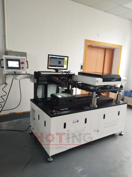
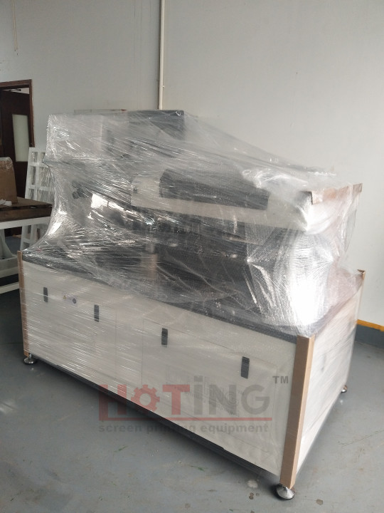


Thick film screen printer with CCD auto registration delivery never stop. This screen printer widely used in Ecigarette lighter ceramic heater sheet, Porous ceramic, Ceramic capacitors, Resistors, Thick film circuits, Ceramic circuits, Filters, Glazed potentiometers, Dielectric antennas, Ceramic metallization, RFID, Automotive oil level sensors, Tension sensor, Air quality sensors, Pressure sensors( Piezoresistive, Capacitive), Integrated LED lamp holders, Technical indicators, Piezoelectric ceramic components, LED ceramic substrates, LTCC, MLCC, Optical filter, Ceramic thick film circuit, Solar wafer, Chip components and Electronic parts printing process manufacturing. #printedelectronics #screenprinting
#Thick film screen printer with CCD auto registration delivery never stop. This screen printer widely used in Ecigarette lighter ceramic heat#Porous ceramic#Ceramic capacitors#Resistors#Thick film circuits#Ceramic circuits#Filters#Glazed potentiometers#Dielectric antennas#Ceramic metallization#RFID#Automotive oil level sensors#Tension sensor#Air quality sensors#Pressure sensors( Piezoresistive#Capacitive)#Integrated LED lamp holders#Technical indicators#Piezoelectric ceramic components#LED ceramic substrates#LTCC#MLCC#Optical filter#Ceramic thick film circuit#Solar wafer#Chip components and Electronic parts printing process manufacturing.#printedelectronics#screenprinting
0 notes
Last Seen Blogs

meeeowns
neth✿

purpurestudio-blog
Purpure Studio

drpandatea-blog
you should feel what I feel


medohxamaligame
Silly Lil' Games