#Dielectric antennas
Text
Dielectric Resonator Antenna Market Key Drivers, Challenges, and Prominent Regions by 2032
Dielectric resonator antennas (DRAs) are advanced components used in wireless communication systems to provide high-performance signal transmission and reception. Unlike traditional antennas, DRAs utilize a dielectric resonator material to achieve compact size, high efficiency, and wide bandwidth. This makes them ideal for applications requiring high-frequency operation and compact form factors.
The dielectric material used in DRAs allows for precise control of the antenna's resonant frequency and impedance, resulting in enhanced performance characteristics such as improved gain, directivity, and bandwidth. DRAs are commonly used in applications including telecommunications, satellite communication, and radar systems.
The Dielectric Resonator Antenna Market is expected to witness substantial growth, reaching significant value by 2031 ,with a projected Compound Annual Growth Rate (CAGR) of 5.1% from 2024 to 2031.
Future Scope
The future of dielectric resonator antennas is characterized by continued innovation in materials and design techniques. Advances in dielectric materials and fabrication processes will enable the development of even more compact and efficient antennas, suitable for emerging wireless technologies and high-frequency applications.
The integration of DRAs with advanced technologies such as 5G and millimeter-wave communications is expected to drive further development. DRAs will play a crucial role in meeting the demanding requirements of next-generation wireless systems, offering enhanced performance and reliability.
Trends
Several key trends are shaping the development of dielectric resonator antennas. One significant trend is the growing demand for high-frequency and high-data-rate communication systems, driven by the proliferation of 5G and future 6G technologies. DRAs are well-suited for these applications due to their ability to operate at higher frequencies with minimal loss.
Another trend is the focus on miniaturization and integration. As electronic devices become more compact, there is a need for smaller and more efficient antennas that can be integrated into portable and wearable devices without compromising performance.
The development of advanced dielectric materials and innovative designs is also a key trend, enabling DRAs to achieve better performance metrics and meet the evolving requirements of modern communication systems.
Applications
Dielectric resonator antennas are used in a wide range of applications across telecommunications, satellite communication, and radar systems. In telecommunications, DRAs are employed in base stations, mobile phones, and other wireless devices to ensure high-quality signal transmission and reception.
In satellite communication, DRAs are used in ground stations and satellite terminals to achieve reliable and high-frequency communication. In radar systems, DRAs provide precise signal detection and tracking capabilities, enhancing the performance of various radar applications.
Solutions and Services
Manufacturers of dielectric resonator antennas offer a range of solutions including custom-designed DRAs, high-performance dielectric materials, and integrated antenna systems. These solutions are tailored to meet the specific requirements of different applications and environments.
Support services typically include design consultation, prototyping, testing, and integration to ensure that DRAs meet performance and quality standards. Manufacturers also provide ongoing technical support and maintenance to optimize the performance and reliability of dielectric resonator antennas.
Key Points
Dielectric resonator antennas provide high-performance signal transmission and reception with compact size and wide bandwidth.
Future developments include advanced materials, integration with 5G and millimeter-wave communications, and miniaturization.
Trends include high-frequency applications, compact design, and innovative materials.
Applications span telecommunications, satellite communication, and radar systems.
Solutions and services encompass custom designs, high-performance materials, and technical support.
Read More Details: https://www.snsinsider.com/reports/dielectric-resonator-antenna-market-4225
Contact Us:
Akash Anand — Head of Business Development & Strategy
Email: [email protected]
Phone: +1–415–230–0044 (US) | +91–7798602273 (IND)
0 notes
Text
things i learned this year on wikipedia: you can microwave metal actually
there is an ancient (ANCIENT) microwave in my work breakroom. you could fit an entire turkey in there. there's no turntable, if your food ends up uneven that's on you. And, most mysterious of all: it has a metal rack in the center of the microwave.

(example image from wikipedia)
after spending 4 years at this place avoiding the Big Microwave and its Probable Death Rack i finally went on wikipedia and made a discovery. I had been lied to my entire life. You can put metal in the microwave.
It's the shape that gets you, not just the material. It's just that you can only put things without points in the microwave, which rules out almost all metal items you were potentially thinking of microwaving. Unless you have a metal orb at home. that might be okay. Quothe wikipedia:
Contrary to popular assumptions, metal objects can be safely used in a microwave oven, but with some restrictions.[77][78] Any metal or conductive object placed into the microwave oven acts as an antenna to some degree, resulting in an electric current. This causes the object to act as a heating element. This effect varies with the object's shape and composition, and is sometimes utilized for cooking.
Any object containing pointed metal can create an electric arc (sparks) when microwaved. This includes cutlery, crumpled aluminium foil (though some foil used in microwave ovens is safe, see below), twist-ties containing metal wire, the metal wire carry-handles in oyster pails, or almost any metal formed into a poorly conductive foil or thin wire, or into a pointed shape.[79] Forks are a good example: the tines of the fork respond to the electric field by producing high concentrations of electric charge at the tips. This has the effect of exceeding the dielectric breakdown of air, about 3 megavolts per meter (3×10⁶ V/m). The air forms a conductive plasma, which is visible as a spark. The plasma and the tines may then form a conductive loop, which may be a more effective antenna, resulting in a longer lived spark. When dielectric breakdown occurs in air, some ozone and nitrogen oxides are formed, both of which are unhealthy in large quantities.
#mine#every person i've explained this to has never heard it#apparently we decided the facts were too complicated#and kept the entire population at a microwave 101: DonT Forks#someone should add this to the wikipedia common misconceptions article bc I have read that several times#and this did not appear
24 notes
·
View notes
Text

Ancient temple with a Dielectric Resonator Antenna. (They insulate as well as osculate) This holds frequency better than any metal modern counterpart.
Borobudur is a temple that took over 100 years to build, from the time of Rakai Mataram Ratu Sanjaya (717-745) until it was completed in 825 and inaugurated during the reign of Sri Maharaja Samarottungga (782-835)
8 notes
·
View notes
Text
Tips to design High Frequency PCB for optimal performance
Best Practices for High-Frequency PCB Design
We all know the importance of military electronic devices like military radars, satellite systems, communications, etc, for the safety of our country. But do you know that these systems consists of high-frequency Printed Circuit Boards? Therefore, a high-frequency printed circuit board (PCB) requires careful design to guarantee the best performance. As a PCB producer or user, you must know that even little errors can have a big effect on performance.
Here, in this insightful blog, we will discuss negotiating the challenges of high-frequency PCB design so that your product development project performs as intended.
Understanding the Basics
It is essential to understand why high-frequency PCBs need particular care before going into the details. Signals can deteriorate at high frequencies for reasons including crosstalk, signal reflection, and impedance mismatches. PCB design guidelines are helpful in reducing these problems and guaranteeing the effective operation of your printed circuit board.
Key Design Considerations
These super-critical High-Frequency Printed Circuit Boards need several careful considerations at every stage, from the design to production. Here are some noteworthy points to keep in mind.
Material Selection
Maximizing the performance of your PCB starts with selecting the appropriate material. FR4, Rogers, or Teflon (PTFE) are common materials used in high-frequency PCBs and have distinct
advantages:FR4: Lower dielectric losses but more expensive
Rogers: Consistent high-frequency performance with reduced dielectric losses.
Teflon or PTFE: Excellent performance, yet processing is more difficult and costly.
Picking the right material will depend on the specifications and budget of your project.
Layer Stack-Up
Your PCB's layer stack-up affects signal integrity. Signal integrity is improved, and loop regions are reduced when power and ground planes are close to signal layers. With the balanced layer stacking, electromagnetic interference (EMI) can be reduced in high-frequency designs.
Impedance Control
High-frequency PCB design depends critically on maintaining constant impedance. Mismatched impedance often results in lost and reflected signals. Controlled impedance traces are computed using the material's dielectric constant, trace width, and height. There are tools and software accessible to assist you in creating and validating impedance-controlled traces.
Being one of the market leaders in the PCB manufacturing industry, we at PCB Power apply these considerations to produce advanced high-frequency printed circuit boards.
Practical Tips for High-Frequency PCB Design
Here are some simple yet effective practical tips that can improve your PCB performance.
Using Shorter Trace Lengths: A shorter trace length can help reduce signal deterioration. Long traces can function as antennas, absorbing noise and producing EMI problems. Reduce the distance high-frequency signals must travel over the PCB.
Avoid Sharp Bends: Impedance alterations and signal reflection are two effects of abrupt bends in traces. To maintain signal integrity, use 45-degree angles or gentle curves rather than 90-degree turns.

The Right Grounding: It takes a strong grounding plan. To reduce noise and performance enhancement, use a ground plane to give signals a return route. Narrow ground traces are to be avoided since they can cause inductance and lower signal quality.

Advanced Techniques:
With technological advancement, new and modern techniques are implemented for high-frequency printed circuit board manufacturing.
Via Placement
High-frequency signals can be impacted by parasitic inductance and capacitance. To reduce the effect, use vias sparingly and put them thoughtfully. Use several vias to disperse the current equally as needed.
Differential Pair Routing
Differential pair routing helps lower noise and crosstalk for fast signals. Signal integrity must be preserved by routing differential pairs closely together with identical lengths.

Testing and Validation
Test and validate your high-frequency PCB thoroughly after it is designed. Test impedance and signal integrity with Time Domain Reflectometry (TDR) and Vector Network Analyzers (VNA). Furthermore, simulation software is highly useful for predicting PCB performance under different circumstances.
FINAL WORDS:
High-frequency printed circuit board design calls for meticulous attention to detail and following particular PCB design standards. High-frequency applications can be optimized on your PCB by choosing the appropriate materials, keeping impedance control, and putting in place efficient grounding and routing techniques. To be sure your design satisfies performance objectives, never forget the need for extensive testing and validation.
By using these tips, you can confidently take on the difficulties of high-frequency PCB design and guarantee that your projects meet the best possible performance and dependability criteria.
To learn more about printed circuit boards, please visit our resource page. Connect with us through [email protected] or call us at +1(818)8868900.
This Blog Originally Posted Here: Tips to design High Frequency PCB for optimal performance
0 notes
Text

Aluminum Nitride Ceramic PCB
Aluminum Nitride (AlN) is currently the best ceramic substrate material accessible. Its properties of high thermal conductivity (170 W/mK) combined with being a strong dielectric and a low expansion rate (CTE) make it the material of choice today as a substrate or package for high-power LEDs, ICs, sensors and many other components and circuits.
Reasons why you should choose Aluminum Nitride PCB for your project
Aluminum Nitride (AlN) PCBs offers several compelling reasons, especially in applications where thermal management, high-frequency performance, and reliability are critical. Here are some key reasons to consider using AlN PCBs:
·Exceptional Thermal Conductivity: AlN ceramics have excellent thermal conductivity properties, making them highly effective at dissipating heat generated by electronic components. This property is crucial for maintaining component reliability, extending the lifespan of electronics, and preventing overheating-related failures.
·High-Frequency Performance: AlN PCBs exhibit low signal loss and minimal signal distortion, making them well-suited for high-frequency and microwave applications. They provide reliable signal transmission and are ideal for RF (Radio Frequency) circuits, microwave antennas, and advanced communication systems.
·Electrical Insulation: AlN ceramics possess excellent electrical insulation properties. They have a high dielectric strength, preventing electrical leakage and ensuring the isolation of electrical components and signals. This insulation is essential for maintaining signal integrity and preventing unintended electrical connections.
·Mechanical Strength: AlN ceramic substrates have good mechanical strength, with the ability to withstand mechanical stresses during manufacturing, assembly, and operation. This mechanical robustness contributes to the overall reliability of electronic systems.
·Compatibility with Semiconductor Devices: The thermal expansion coefficient of AlN is relatively close to that of silicon, a common material used in semiconductor devices. This compatibility allows for efficient heat transfer from semiconductor components, reducing the risk of thermal stress and enhancing their performance and longevity.
·High-Power and High-Temperature Applications: AlN PCBs are well-suited for high-power electronic components and high-temperature environments. They can efficiently dissipate heat from power amplifiers, voltage regulators, LEDs, and other heat-generating devices.
·Longevity and Reliability: The superior thermal management provided by AlN PCBs contributes to the longevity and reliability of electronic systems, reducing the risk of premature component failures due to overheating.
·Wide Range of Applications: AlN PCBs find application in various industries, including aerospace and defense, telecommunications, medical devices, automotive, and industrial electronics. They are versatile and suitable for demanding electronic applications.
·Customization: AlN PCBs can be customized to meet specific design requirements, including layer count, dimensions, and design layout, ensuring that they are tailored to the needs of the application.
·Efficient Heat Dissipation: The exceptional heat dissipation properties of AlN PCBs allow for the effective management of thermal issues without the need for additional cooling mechanisms, such as heat sinks or fans.
In conclusion, choosing Aluminum Nitride (AlN) PCBs offers lots of advantages, including superior thermal conductivity, high-frequency performance, electrical insulation, and mechanical strength. These properties make them a preferred choice in applications where traditional PCB materials may not meet the stringent requirements for thermal management and reliability. At Hitech Circuits, we supply both Aluminium Nitride PCB (AlN) processed by thick film process (Silver/silver palladium metalization) as well as Direct Plated Copper Technologies (DPC), with copper tracks and pads.
#AINPCB #ceramicpcb
0 notes
Text
0 notes
Text
0 notes
Text
Liquid Crystal Polymers (LCP) Market: Riding the Wave of Innovation
Liquid Crystal Polymers (LCP) have emerged as a transformative force in the materials industry, offering a unique blend of properties that cater to diverse applications. This research blog delves into the dynamic landscape of the Liquid Crystal Polymers market, exploring its market size, demand drivers, growth factors, and the exciting possibilities it presents across various sectors.
Market Size:
The Liquid Crystal Polymers market has experienced remarkable growth, driven by the increasing demand for high-performance materials in sectors such as electronics, automotive, and aerospace. The market’s size is influenced by the escalating need for lightweight, durable, and heat-resistant materials. LCP’s ability to excel in extreme conditions positions it as a material of choice for cutting-edge applications.
Demand Drivers:
Electronics Revolution: The relentless pace of innovation in the electronics industry has fueled the demand for materials that can meet stringent performance requirements. Liquid Crystal Polymers, with their excellent electrical properties, dimensional stability, and resistance to high temperatures, have become integral to the production of connectors, sockets, and other electronic components.
Automotive Advancements: As the automotive industry undergoes a paradigm shift towards electric vehicles and lightweighting, LCP finds increasing use in critical components such as sensors, connectors, and under-the-hood applications. The material’s ability to enhance fuel efficiency and withstand harsh conditions makes it a valuable asset in the pursuit of automotive innovation.
Telecommunications Evolution: The rollout of 5G technology has heightened the demand for materials that can facilitate high-frequency data transmission. Liquid Crystal Polymers, with their low dielectric constant and excellent signal integrity, play a crucial role in the development of antennas, connectors, and other components vital for the 5G infrastructure.
Growth Factors:
Material Advancements: Ongoing research and development efforts are focused on enhancing the properties of Liquid Crystal Polymers, expanding their application spectrum. Innovations in formulation and processing techniques are opening up new possibilities for LCP in areas such as 3D printing and advanced manufacturing.
Global Connectivity: The increasing interconnectedness of global markets provides opportunities for LCP manufacturers to reach a wider audience. As industries worldwide recognize the advantages of LCP in various applications, the market is poised for continued growth on a global scale.
Sustainable Solutions: The growing emphasis on sustainability and environmental consciousness is driving the adoption of eco-friendly materials. Liquid Crystal Polymers, with their recyclability and potential for reducing energy consumption, align with the sustainability goals of many industries.
Future Prospects:
The future of the Liquid Crystal Polymers market looks promising, with ongoing technological advancements and the material’s adaptability to evolving industry needs. As industries continue to push the boundaries of innovation, Liquid Crystal Polymers are expected to play a pivotal role in shaping the next generation of high-performance materials.
Conclusion:
In conclusion, the Liquid Crystal Polymers market is thriving in the midst of technological revolutions and industry transformations. Stakeholders and businesses keen on staying ahead in the materials landscape should closely monitor the evolving trends and capitalize on the versatile capabilities that Liquid Crystal Polymers bring to the table. The journey ahead promises exciting possibilities as LCP continues to ride the wave of innovation.
0 notes
Text
Global 3D Printed Electronics Market Size, Share, Growth Analysis, By Printing Technology(Inkjet Printing Screen Printing, Gravure Printing), By Material(Ink, Polymer)
Global 3D Printed Electronics Market Insights
Global 3D Printed Electronics Market size was valued at USD 10.6 billion in 2021 and is poised to grow from USD 12.22 billion in 2022 to USD 38.2 billion by 2030, growing at a CAGR of 15.31% in the forecast period (2023-2030).
3D printed electronics is a new program that allows electronics to be integrated into or on top of devices. The concept of 3D printing has been widely applied to the exterior of 3D injection molded synthetic objects to add antennas and simple conductive interconnects. With technological advancements in the 3D printed electronics business, new techniques can be used to create materials and processes to create sophisticated circuitry inside parts. Customization can be a valuable advantage in the development of fully formed additive manufacturing parts for circuit boards or any computerized device. The demand for small, thin devices with advanced capabilities is insatiable. However, difficult tasks such as designing a PCB or printed circuit board and its components are usually outsourced, resulting in longer waiting times. With the introduction of 3D printing, it is now possible to create in-house prototypes of circuits and circuit boards, reducing cost, time, and concerns about intellectual property infringement. Improved efficiency and productivity of manufacturers, as well as lower material costs, are expected to drive the global 3D printed electronics market during the forecast period.
Increased production of products with reduced weight, ease of use, and improved technology in manufacturing electrical components, all benefit the market. Increased production of antenna and sensor printing in 3D form stimulates the market. The rapid adoption of newly developed technologies in many sectors, as well as increasing consumer demand in industries such as the health sector, defence, telecommunication, automobile industry, electrification system, power utility, aerospace, and many others. The market is expected to flourish with the increased competition due to new arrivals and the availability of increased performance. Rising market participants and increased investment in the electronics and automobile industries have boosted market rates. However, the cost of new equipment and material for printed electronics are high, may this factor hamper market growth.
Global 3D Printed Electronics Market Segmental Analysis
Global 3D printed electronics market is segmented on the basis of printing technology, material and region. On the basis of printing technology, global 3D Printed Electronics Market is segmented into inkjet printing, screen printing, gravure printing, and flexographic printing. On the basis of material, global 3D Printed Electronics Market is segmented into ink, polymer, paper and glass. On the basis of region, global 3D Printed Electronics Market is divided into North America, Europe, Asia Pacific, Latin America, and MEA.
3D Printed Electronics Market Analysis by Printing Technology
On the basis of printing technology, global 3D printed electronics market is segmented into inkjet printing, screen printing, gravure printing, and flexographic printing. The inkjet segment accounted for a significant share of the revenue in the global market. The rapidly increasing adoption of this unique and advanced technology is fuelling the rapid growth of this segment. Inkjet printers are adjustable and versatile and easy to set up. Inkjet printers have a low throughput of about 100 m2/h and low resolution (about 50 m). It works well with soluble, low-viscosity materials such as organic semiconductors. High-viscosity materials, such as organic dielectrics, and dispersed particles, such as inorganic metal inks can cause nozzle obstruction. The thickness and uniformity of the dispersion decrease as the ink is applied in droplets. Using multiple nozzles simultaneously and pre-forming the substrate can improve productivity and resolution.
3D Printed Electronics Market Analysis by Material
On the basis of material, global 3D printed electronics market is segmented into ink, polymer, paper and glass. The ink materials segment accounted for the largest revenue share in the printed electronics market. The increasing growth of this segment is due to the rapid market acceptance of this substance. The increasing adoption of printed electronics technology has allowed the widespread use of inks in a wide range of applications in many fields. Also, inks are becoming more readily available in the market, making them more accessible to buyers.
0 notes
Text
For constantly changeable phase, which is typically regulated by a voltage, analogue phase shifters are utilised. Varactor diodes or nonlinear dielectrics are used in electrically controlled phase shifters. The main purpose for analogue phase shifters is in phased array antennas, which are utilised in weather radars and satellites for military equipment.
Analog phase shifters have long been used in a small number of satellite communication and radar applications, with the defence industry accounting for a sizable portion of the market. This market situation is expected to alter in the upcoming years as 5G antennas use analogue phase changers. The market for analogue phase shifters will experience a significant increase due to the pervasive and ubiquitous nature of communications infrastructure.
0 notes
Text
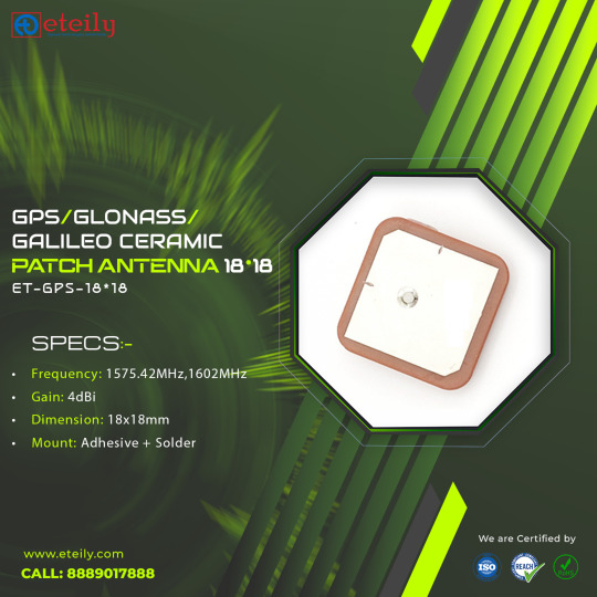
GPS/GLONASS/GALILEO CERAMIC PATCH ANTENNA
Eteily's Ceramic Patch Antenna is a low profile, dielectric antenna element specifically designed for 1575.42MHz L1 GPS, 1602MHz GLONASS & Galileo L1 1575.42MHz applications.The flat patch antenna incorporates a Square design for GPS right-hand circular polarization wave reception. These antennas has excellent stability and sensitivity through the use of high performance ceramic materials well suited for GPS applications and ships with double-sided adhesive tape for ease in mounting to the ground plane.
GPS-GNSS ANTENNA
A GPS-GNSS antenna is designed specifically for Global Positioning System (GPS) and Global Navigation Satellite System (GNSS) applications. These antennas receive signals from a constellation of satellites to determine precise positioning, velocity, and timing information. We are also manufacturer and suppliers of GPS GNSS antenna in Delhi, Mumbai, Chennai, Hyderabad, Pune, Bangalore, Kolkata and Ahmedabad.
Eteily is the world class manufacturer of GNSS Global Navigation Satellite System Antenna, which includes GPS, GLONASS, Galileo, BeiDou IRNSS Antennas for navigation tracking. We design for various applications such as GPS Tracker, Marine application, Railway Application, Asset Tracking and many more.
#High Performance GPS Antenna#GPS Antenna by Eteily-Excellent Performance#GPS antenna manufacturer in india#GPS antenna manufacturer in china#GPS antenna#Global Positioning System Antenna manufacturers#Gps Patch Antenna#GPS antenna manufacturer#Top Gps Antenna Manufacturers#Top Gps Antenna Manufacturers in india#GPS Antenna Types#gps antenna price in india#gps antenna design#gps antenna in telecom#gps antenna for mobile phones#Gps Active Antenna Manufacturers#GPS Marine Antenna Manufacturer#GPS & GNSS Antennas#GPS Internal & External Antennas#GPS Antennas and Accessories#Garmin GPS Antenna#GPS Antenna Price#gps antenna for car#GPS Receiver & Antenna#gps tracker antenna#gps pcb antenna#gps antenna supplier in india#gps suppliers in india#Top Gps Tracking Device Manufacturers in india
0 notes
Text
Rocket-PCB: Unleashing the Potential of Ceramic PCBs
Rocket-PCB is proud to introduce its latest innovation in the world of printed circuit boards (PCBs) — Ceramic PCBs. This cutting-edge technology brings a host of advantages over traditional PCB materials, opening up new possibilities for various industries. In this article, we will delve into the benefits and applications of Ceramic PCBs, highlighting their role in revolutionizing electronic design and manufacturing.

Advantages of Ceramic PCBs:
Excellent Thermal Performance: Ceramic PCBs exhibit outstanding thermal conductivity, making them ideal for high-power applications. The excellent heat dissipation properties ensure efficient cooling of electronic components, reducing the risk of overheating and improving overall system reliability.
Enhanced Electrical Performance: With low dielectric loss and minimal signal attenuation, Ceramic PCBs enable high-frequency circuit designs, making them suitable for RF/microwave applications. Their low electrical impedance contributes to better signal integrity and reduced electromagnetic interference.
High Mechanical Strength: The robustness and durability of Ceramic PCBs make them resistant to mechanical stress and vibration, ensuring long-term stability even in harsh environments. This makes them ideal for applications in aerospace, automotive, and industrial sectors.
Compact and Lightweight: The compact nature and lighter weight of Ceramic PCBs allow for miniaturization of electronic devices. This aspect is particularly advantageous in portable gadgets and wearables where space and weight are critical factors.
Applications of Ceramic PCBs:
Power Electronics: Ceramic PCBs find extensive use in power electronic devices such as power amplifiers, motor controllers, and high-power LED drivers. Their exceptional thermal properties help optimize power dissipation and maximize the efficiency of these systems.
RF/Microwave Devices: The high-frequency capabilities of Ceramic PCBs are well-suited for designing antennas, radar systems, satellite communications, and wireless transceivers. Their low loss tangent ensures minimal signal distortion and high performance in communication applications.
LED Technology: Ceramic PCBs enhance the performance of LED technology by providing efficient thermal management, leading to improved brightness and extended lifespan of LED products.
Automotive Electronics: The automotive industry benefits from the reliability and thermal stability of Ceramic PCBs in electric vehicles (EVs), battery management systems, and automotive lighting systems.
Medical Devices: In medical electronics, Ceramic PCBs play a crucial role in devices like implantable medical sensors, pacemakers, and ultrasound equipment, where reliability and long-term stability are paramount.
Rocket-PCB’s Ceramic PCBs bring a new era of possibilities to the world of electronic design and manufacturing. With their outstanding thermal conductivity, electrical performance, and mechanical strength, these PCBs cater to a wide range of industries, from aerospace to medical applications. As technology continues to evolve, Ceramic PCBs will undoubtedly play a pivotal role in shaping the future of electronic devices, enabling more efficient, compact, and reliable solutions. Embrace the power of innovation with Rocket-PCB’s Ceramic PCBs and take your electronic designs to new heights.
0 notes
Text
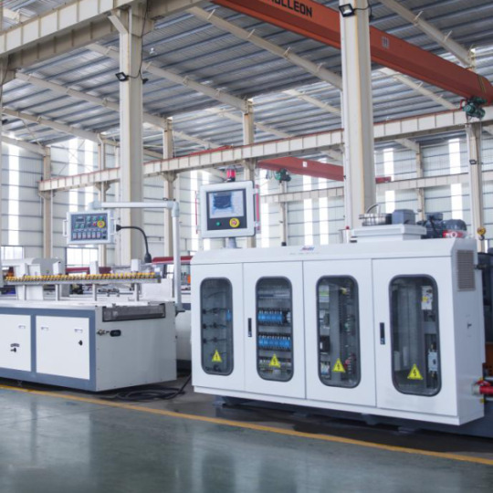
5G Radome Extrusion Machine
The function of radome is to protect the antenna system from the influence of external environment (such as wind, snow, sunlight, biology, etc.), prolong the service life of antenna, and ensure the permeability of electromagnetic wave. Therefore, the radome material shall meet the requirements of dielectric performance, mechanical performance, weather resistance, manufacturability and weight.
On this basis, the requirements for 5g radome are as follows
1. Low dielectric and low loss
While the radome plays a protective role, the dielectric properties of the material will also directly affect the performance of the antenna. The absorption and reflection of electromagnetic waves by materials will reduce the signal transmission efficiency. Therefore, radome materials need to adopt materials with low dielectric constant and low dielectric loss, and millimeter waves are easier to be lost, so the requirements for dielectric properties of materials are higher. At present, it is urgent to develop low dielectric and low loss materials for radome.
2. Lightweight
The radome is usually made of fiber reinforced resin composites. At present, the radome is mainly made of FRP, but the proportion of FRP is large, which is not conducive to the lightweight design of the antenna. The new material of Huawei radome is gfrpp, i.e. super strong glass fiber reinforced polypropylene resin, which is 40% lighter than the traditional FRP, and the weight of multi frequency antenna is controlled within 50kg, Avoid antenna hoisting to save installation time and cost. Therefore, in order to meet the design needs of lightweight, integration and miniaturization of 5g antenna, radome materials will also develop to lightweight.
3. Environmental protection
In recent years, with the enhancement of people's awareness of environmental protection, the requirements for environmental protection at home and abroad are higher and higher. Environment-friendly is the higher requirements of 5g for radome materials. Enterprises actively research and develop low dielectric and low loss reinforced and modified materials with high cost performance, environment-friendly and lightweight, such as ASA, PP, PC and other materials
With the advent of 5G era, the fast development of radome for base-station protection is promoted with material and related equipment. The traditional FRP radome can not satisfied with the relevant requirements. PVC radome has some application to certain extent. However, with some testing and application of new materials, such as PC + glass fiber, PP + glass fiber, ASA etc, the main advantages are: low dielectric, low cost, light-weight, environmental.
According to the market demand, Jwell has researched,developed and launched: PVC, PC + glass fiber, PP + glass fiber, ASA radome extrusion machine line.
Main technical specification
Model
SJZ65
SJZ80
JWS90
JWS100
Screw(mm)
65/132
80/156
90/33
100/33
Output(kg/h)
150-200
250-350
120-150
150-200
Motor power(kw)
37
55
75
110
Product image display
Read the full article
0 notes
Text

What is Rogers PCB?
Rogers PCB is a type of printed circuit board (PCB) material made from a combination of epoxy and ceramic. It is well known for its high dielectric constant, low loss tangent, and high thermal conductivity, making it an ideal material for high-frequency applications. It is used in a wide range of electronics, such as:
5G Station
Cellular Base Station Antennas and Power Amplifiers
Automotive Radar and Sensors
Microwave point to point (P2P) links
LNB’s for Direct Broadcast Satellites
Microwave equipment of all kinds.
RF Identification (RFID) Tags
Rogers PCB is produced using the raw materials of the Rogers Company. Rogers company manufactures the laminate materials that are often used for manufacturing circuit boards. The Rogers PCB is a type of high-frequency PCB board, quite different from the traditional PCB board materials, epoxy resin. It uses the ceramic base as the material of high frequency. The major advantage of Rogers PCB is the temperature stability and superior dielectric constant.
Rogers PCB has a major application in high-speed electronic designs, radio frequency applications, and commercial microwaves. The low water absorption capacity of this Rogers PCB is ideal for the application of high humidity. Other Rogers PCB applications include RF identification tags, power amplifiers, automotive radar, sensors, etc.
Rogers PCB fabrication needs in-depth research on high-frequency PCB. HITECHPCB is a Rogers PCB manufacturer and has a deep understanding of the performance of Rogers PCB material. For example, Rogers PCB laminates and Rogers PCB dielectric constant in Rogers PCB material properties Rogers PCB is a high-frequency PCB material model produced by Rogers company, different from the conventional FR-4 PCB material. There is no epoxy resin in the Rogers PCB material, and Rogers ceramic PCB is used as the High-frequency PCB material. Absorption of Rogers PCB, it can be used as an ideal choice for application ns in high humidity environments, providing customers in the high-frequency PCB industry with the highest quality.
Difference Between Rogers Materials and FR-4 Materials
By combining Rogers PCB layers with FR-4 layers, we can achieve reduced cost and maximum performance compared to if we used only Rogers layers. Thus, this process should use Rogers PCB cores instead of prepregs for this process.
FR-4 stack up with 6 layers is shown below. Because prepreg is less expensive than cores, it is placed on the outside to minimize cost. A foil build is often referred to as this.
Rogers layers are required on the outside layers, but the core is usually found on the layers that need them. Below is an example with 6 layers but with 3 cores instead of 2. This configuration is sometimes called a "core build" or "cap construction" board. Rogers PCB is a high-frequency circuit board that has ceramic laminates and reinforced hydrocarbon. A Rogers PCB may be made from cores and prepregs, but most often, the top two copper layers are carried on the core, while the rest of the board is made from standard FR-4 to reduce the cost. The PCB materials absorb the signal, due to which it has less signal loss compared to that of FR-4. At higher frequencies, the signal loss is greater in FR-4 materials. This is also the signal length and design dependent.
High-Frequency
PCB with FR-4 materials is preferred due to their low cost, reliability, and well-understood electrical and mechanical properties. They are used in various applications ranging from microwave designs to audio circuits. Unfortunately, FR-4 printed circuit boards are not suitable for high-frequency applications. Rogers created the most well-known high-frequency-special laminates. Its materials have a constant dielectric reduction of close to 20% when compared to FR-4 printed circuit boards.
The best way to determine whether your project will benefit from high-frequency laminates is to assess electrical and mechanical requirements. If you find both variations are too broad, Rogers PCB material is a better option.
Dissipation
The material used is most important when producing printed circuit boards, though it may require a high cost. However, it is not the only issue that knows the content value when it comes to the loss factor or Df. FR-4 printed circuit boards will be affected or reduced. The losses are greater when compared to printed circuit boards made from Rogers materials.
In other words, when compared to Rogers PCB, FR-4 materials have a higher dissipation factor, especially at high frequencies. Typical values for FR-4 printed circuit boards are around 0.020 and close to 0.004 for Rogers boards. Dissipation of FR-4 materials increases with frequency. High-frequency laminates primarily have a frequency-dependent stable dissipation characteristic.
The signal loss is minimized with the lower dissipation factor in FR-4. Also, the automated assembly process and the processing of FR-4 materials make them easier in the assembly and manufacturing process.
Impedance Stability
Impedance is the measure of the current opposition when applying voltage. In many design applications, the stable impedance is essential and is an area where the materials like Rogers and FR-4 are applied.
FR-4, despite its low cost, is prone to high variations in the dielectric constant with the change in temperature across the length and width of the substrate. In terms of impedance stability, Rogers' material has a wider range of dielectric constants than FR-4 content.
High-frequency laminates are preferable for circuits that require little variation over wide temperature ranges. In this case, you may need to use printed circuit boards made of Rogers materials rather than FR-4 materials, especially if most of your operations involve working in high-temperature environments.
Dielectric Constant
The dielectric constant of any material measures a substance's ability to store some electrical energy across an electrical field. When it comes to dielectric constant, FR-4 has a dielectric constant of about 4.5, which is much lower than Roger's material, which has a dielectric constant of about 6.15 to 11.
The dielectric constant of FR-4 is comparatively higher than that of plastic materials. Using FR-4 materials can save at least 25% of PCB made from such materials. Other factors that make FR-4 articles available include their lightweight, moisture resistance, and high dielectric strength. Even though the Rogers PCB has a higher dielectric than FR-4, you can go with FR-4. FR-4 and Rogers 4350b and 4350 are similar manufacturing processes, although FR-4 stores electrical energy effectively.
Thus, PCB with higher dialect trends breaks easier when subjected to intense electric fields.
0 notes
Text
Versatile Components for Industrial Applications
Steatite Ceramic Spacers are essential components used in a wide range of industrial applications. These spacers are made from steatite, a magnesium silicate material that possesses excellent electrical insulation and thermal resistance properties. With their unique characteristics, Shunt Reactor play a crucial role in supporting and spacing various electronic components, circuit boards, and systems operating in high-temperature environments.
One of the key features of steatite ceramic spacers is their exceptional electrical insulation properties. Steatite has a high dielectric strength, which means it can withstand high voltages without conducting electricity. This makes it an ideal material for creating insulating barriers between conductive components, ensuring the safe and reliable operation of electrical systems. Steatite ceramic spacers effectively prevent electrical leakage and short circuits, reducing the risk of damage and improving overall system performance.
In addition to their electrical insulation properties, steatite ceramic spacers also exhibit excellent thermal resistance. Steatite has a low coefficient of thermal expansion, meaning it can withstand significant temperature variations without cracking or deforming. This makes ceramic spacer heat shield suitable for applications in high-temperature environments, such as heating elements and industrial ovens. They provide thermal insulation and help maintain stable temperatures, preventing heat transfer and ensuring the efficient operation of the system.
The mechanical strength of steatite ceramic spacers is another notable characteristic. Steatite is a hard and durable material that can withstand mechanical stress and vibrations. This makes it suitable for use in structural supports, where the spacers provide stability and maintain proper alignment of components. Steatite spacers can withstand significant loads and pressures, ensuring the longevity and reliability of the supported system.
Furthermore, ceramic spacers for resistor to chemical corrosion. They are unaffected by most acids, alkalis, and organic solvents, making them suitable for applications in chemically harsh environments. This corrosion resistance ensures the longevity of the spacers and prevents degradation or failure due to chemical exposure.
The versatility of steatite ceramic spacers is evident in their diverse range of applications. In the electronics industry, these spacers are commonly used in circuit boards to separate and support components, preventing contact between conductive elements and providing electrical insulation. They are also used in power distribution systems to maintain proper spacing between high-voltage conductors, reducing the risk of electrical arcing or short circuits.

Steatite spacers find applications in heating elements, where they provide electrical insulation and mechanical support. They help maintain the integrity of the heating element, ensuring efficient heat transfer and preventing electrical faults.
Moreover, steatite ceramic spacers are used in high-temperature applications such as industrial furnaces, kilns, and incinerators. They serve as supports for heating elements and other components, maintaining their structural integrity in extreme heat conditions.
ceramic spacer manufacturers are also utilized in the automotive industry, particularly in ignition systems. They provide electrical insulation and support for spark plugs, helping to create reliable electrical connections and preventing misfires.
In the telecommunications industry, steatite ceramic spacers are used in antennas and waveguides. They ensure proper spacing and alignment of components, optimizing signal transmission and reception.
In summary,
Steatite Ceramic Spacers are critical components with a wide range of industrial applications. Their excellent electrical insulation, thermal resistance, mechanical strength, and chemical corrosion resistance make them indispensable in various systems and environments. Whether in electronics, power distribution, heating elements, or high-temperature applications, ceramic spacers for resistor contribute to the efficient and reliable operation of industrial systems.
Url:- https://www.jyoticeramic.com/Steatitecerami.php
Contact:- +91 253 6918111
Source Link:- https://jyoticeramicc.isblog.net/steatite-ceramic-spacers-versatile-electrical-insulators-37287338
0 notes
Text
0 notes
Last Seen Blogs

transhades
see how it shines

5elementssf
5 Elements Youth Program

muscledaddys
Chestandnipples

thewildestross
XXX~O

airalihsa
Lyna Dewit