#LED ceramic substrates
Text

Scientists study effect of boron nitride microribbon on ceramic properties
In recent years, the high complexity of integrated devices has made heat accumulation increasingly critical and has resulted in higher heat dissipation requirements for substrates and packaging materials. In this study, boron nitride microribbon (BNMR)/Al2O3 composite ceramics are prepared using spark plasma sintering (SPS).
This study examines the effect of varying the amount of toughened phase BNMR on the density, mechanical properties, dielectric constant, and thermal conductivity of BNMR/Al2O3 composite ceramics while also exploring the mechanisms behind the toughening and increased thermal conductivity of the fabricated ceramics.
A team of material scientists led by Ji-Lin Wang from Guilin University of Technology in Guilin, boron nitride microribbon (BNMR)/Al2O3 composite ceramics are prepared using spark plasma sintering (SPS). During the sintering process, the pliable BNMRs were continuously extruded and deformed by the Al2O3 grains under high temperature and pressure, followed by even wrapping of the Al2O3 grains.
Read more.
#Materials Science#Science#Ceramics#Boron Nitride#Composites#Sintering#Boron#Nitrides#Alumina#Aluminum
9 notes
·
View notes
Text
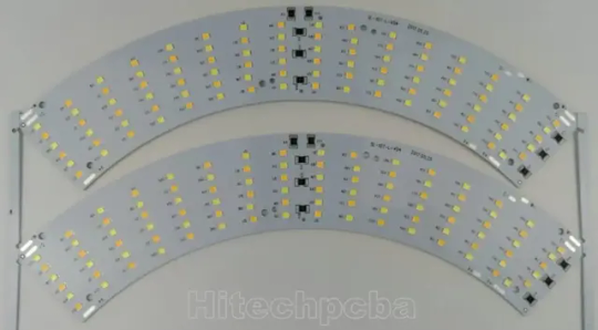
LED PCB Assembly
What is the LED Circuit Board assembly?
Generally, LED PCB assembly is considered to be a circuit board that has the LED components soldered to it. The LED is soldered to the printed circuit board and features a chip that creates the light as electrically connected. A thermal heat sink and a ceramic base are used to bond the chip. Not all the PCB products can be used in Led industry, as an LED PCB is easy to create a high volume of heat, but making it hard to cool with traditional methods. For this reason, metal core PCB is widely used in LED application because of their enhanced ability to dissipate heat, especially aluminum pcb is often used to fabricate PCB for LED lights.
We’ve had great LED PCB assembly experiences with top LED chips to brand such as Cree, Luxeon, Osram, Nichia, Lumileds, MLS, EVERLIGHT, Samsung, LG, Seoul., etc. PCB LED lights can be incorporated into numerous lighting applications due to their combination of excellent energy efficiency, low cost and maximum design flexibility.

Application of LED PCB Assembly
Hitechpcba serves customers in different industries, providing highly reliable and innovative LED PCBs for various applications:
• Horticulture light LED PCB Assembly
• LED controller PCB Assembly
• Computer LED display and indicators
• LED lights PCB Assembly for medical use
• Automotive LED PCBs Assembly include PCBs for brake lights and headlights
• Street lighting LED PCB Assembly
• Flashlights and camping accessories
• Traffic light PCB Assembly
• Commercial lighting LED PCB Assembly
LED PCB Assembly specification
Number of layers for LED PCB
These layers are made up of aluminum and magnesium, but now have Copper base material and Ceramic base materials for LED PCB industry, we can meet it.
Aluminum LED PCBs stand out among other PCBs because it has a good insulation characteristic and has a better machinery performance, the cheap cost is one important factor too.
Types of layers for LED PCB Assembly
Normally, the base layer is made using aluminum alloy metal.
This aluminum alloy substrate used in making the base makes it ideal for through-hole technology which transfers and dissipates heat.
A thermal insulation layer is made using some ceramic polymer which has good viscoelasticity characteristics.
It is highly heat resistant and protects the PCB against heat and mechanical stress.
The circuit layer, which is covered by a copper foil which can range from one to ten ounces.
LED Board type- single or in panel
Some boards are shapeless. For this reason, LED PCB panels are used. This reduces time, labor production and testing time.
Some LED PCB Assembly is done on a single board while others are done on panel boards.
LED PCB Assembly Process
Roughly, the PCBA process can be divided into theses phases: soldering paste printing > SMT (surface mounted technology) > reflow soldering > AOI (automated optical inspection)> THT (through-hole technology) > wave soldering > touch-up and cleaning > IC-programming > FCT (functional tests) > aging testing.
Below we show you the process.
Step1. Summarizing Project Information
Before contacting your supplier, make sure you have all the project information. Suppliers will need info following for quoting LED PCB assembly:
Gerber
BOM
LED PCB specification
Quotation quantity
Once you have gathered these information, you can contact us and request for a quote.
Of course, you can also provide the schematic, LED PCB Assembly pictures and even samples to us. The more details they have, the more accurate the supplier’s quotation will be.
Step2. Discussion and details about custom LED PCB Assembly
Different projects will have different requirements. Remember the special requirements mentioned in step 1? That’s going to be the focus of this session. Equipment and engineering capacity will not be identical between suppliers. Make sure your supplier has the equipment to produce and assemble major components and the corresponding testing capabilities.
For example, some vendors don’t have X-ray testing equipment, which means they can’t check the mount quality of BGA chips. Outsourcing this step will increase risk and cost. That’s what you don’t want.
Also, pay attention to time taken by the supplier to quote. Motherboards often contain hundreds or even thousands of components, and they are supplied by different manufacturers. To ensure the quality of the components, the supplier sourcing team will make multi-inquiries from these manufacturers or authorized suppliers to match customer’s requirement, which usually takes 2-3 business days, and even longer for some scarce chips. Therefore, if your project is complex and the supplier quotes you within few hours, double check with them.
Step3. Sample and feedback
After confirming the PI, the supplier will usually provide pre-production samples for your approval. At the same time, the supplier will also confirm with you the logistics plan of the bulk goods. Make sure they understand your shipping requirements, including details on packaging, customs clearance, taxes, etc.
For us to have a successful LED PCB Assembly process, its functions must be defined. Compliance requirement is defined to reduce the effect when components are selected.
The Bill of Materials is then generated from the information installed on the LED PCB.
All this information is used to assemble components which are identified from MOB to the LED PCB.
After that, the routing of traces is determined to each component, based on the size, shape of the circuit board and location of connectors.

Hitech Circuits is trusted by thousands of electronic engineers on their LED PCB assembly projects, from consumer, led bulb to precisely medical LED light, we can help you from the beginning of design stage; From commercial flood LED to industrial high power LED, from automotive LED to military LED, Venture is the perfect place for your LED PCB assembly requirement.
Hitech Circuits has been participated in hundreds and thousands of LED lighting projects, by providing LED PCB and also LED PCB assembly service.
Our LED PCB assembly had covered both ends of the Lighting Class LED size spectrum, assembling some of the largest (2 meter long boards) and some of the smallest LED Lighting applications which used in Medical Endoscopes.
LED PCB Assembly is very crucial in the current industrial development. Many electrical devises are being innovated and the old once being improved.
LED PCBs are useful due to the fact that they are made using materials that can transfer and dissipate heat. This characteristic increases device durability.
The world is changing with new technology, especially PCB technology that plays an essential role in the application of LED circuits. And the LED industry is taking advantage of this technology and growing faster.
As a full feature PCB solutions provider with more than a decade of experience, we're capable to provide LED PCB fabrication, components procurement and LED PCB assembly all under one roof. We can work with you to develop metal core PCB, aluminum circuit boards customized to your specific applications. We feature competitively priced PCBs made with standard FR-4 material that includes a thermal aluminum clad layer that will efficiently dissipate heat, keep all LED PCB components cool and significantly enhance the performance of your products.

LED pcb board, LED pcb assembly
LED with its advantages of high brightness, high efficiency, low heat, long life, is considered the most development potential in the 21st century lighting. In the market and policy driven by the rapid development of the domestic LED industry blowout has formed a relatively complete industrial chain, including the production of epitaxial wafers, chip preparation, packaging, integration, LED application. In 2010, China's LED industry scale, up from $ 827 billion in 2019 to 220 billion yuan, an annual growth rate of over 70%, higher than the 50% level of growth of the global LED lighting industry output value. Among them, the middle and lower reaches of the most complete industrial chain, accounting for 90% of the overall percentage of the GDP.Chinahas become the world's leading LED manufacturing base and important application market.
To further promote the technological innovation of the LED industry, construction and wide application of independent industry chain, China Electronic Appliance Corporation and industry associations to organize the theme of "Focus on the core energy LED Exhibition will be held November 9-11, 2010 in Shanghai International Expo Center and the 78th China Electronics Fair over the same period will be held will create from raw materials, epitaxial wafers, chip, LED bracket, LED accessories, LED packaging and supporting materials, the LED backlight upstream firm to the upstream and downstream enterprises of the display, lighting, landscaping, decorative lighting, traffic lights, automotive lighting, special lighting, to the equipment, instrumentation, software, finance, consulting and other service enterprises and technological exchanges and market trading platform, help the domestic industry sustained and healthy development, and promote the steady expansion of the LED application market.
In the LED industry chain upstream of the epitaxial wafers and LED chips accounted for 70% of the profits of the whole industry, and technology-intensive, capital-intensive, where the core technology of the LED. Well-known epitaxial wafer and chip production enterprises will be exhibited a number of energy-efficient, low heat, cost-effective LED products, many of whom have excellent products of international advanced level.
LED electronic pcb assembly manufacturing 100% Original LED Chip with one-stop in-house pcba services
3 notes
·
View notes
Text
Understanding Special PCB: The Backbone of Customized Electronics
In today’s rapidly evolving technology landscape, Special PCBs (Printed Circuit Boards) have become a cornerstone in customized electronics, playing a pivotal role in industries like aerospace, healthcare, telecommunications, and automotive. These specialized boards are tailored to meet unique design requirements and performance standards that exceed conventional PCB capabilities.

What are Special PCBs?
Special PCBs are distinct from standard circuit boards due to their specific materials, layout designs, and intended applications. These boards are used for devices that operate in harsh environments, require higher performance, or need to be compact and efficient. Whether it’s rigid-flex PCBs, aluminum-based PCBs for LED lighting, or multilayer boards, special PCBs are designed to cater to niche market needs.
The Role of PCB Manufacturing in Special PCBs
Creating special PCBs demands cutting-edge PCB manufacturing processes and advanced technology. The production of these PCBs involves multiple stages, including:
Design and Prototyping: Advanced software is used to design the layout, followed by the creation of prototypes for testing.
Material Selection: Special materials, such as ceramic, polyimide, or copper-clad laminates, are chosen based on the application’s specific needs.
Precision Assembly: The manufacturing of special PCBs requires high-precision assembly techniques like surface mount technology (SMT) and through-hole assembly to ensure reliability and performance.
PCB Board Makers: Experts in Customization
Leading PCB board makers like Shenzhen Shuoqiang Electronics (SQPCB) specialize in delivering high-quality special PCBs tailored to individual specifications. With state-of-the-art manufacturing facilities, SQPCB can handle small-scale prototype projects or large-scale production orders, ensuring precision, durability, and performance.
Assembly of Special PCBs
PCB manufacturing assembly is a critical phase where components are mounted onto the PCB substrate. For special PCBs, the assembly process requires meticulous attention to detail due to their complexity. Whether it’s high-density interconnect (HDI) boards or PCBs with intricate multilayer designs, the right assembly process ensures the optimal functionality of the circuit.
The PCB assembly process typically involves:
Soldering Components: High-quality soldering methods, like reflow soldering, are used to attach components to the board accurately.
Testing and Quality Control: After assembly, PCBs undergo rigorous testing to ensure they meet quality standards and perform as intended in their specific applications.
Why Choose SQPCB for Special PCB Manufacturing?
SQPCB stands out as a trusted PCB board maker for several reasons:
Customization: Their team of experts works closely with clients to deliver customized special PCBs tailored to specific requirements.
Advanced Technology: They use the latest tools and technologies to ensure the highest standards of manufacturing and assembly.
Quality Assurance: With a robust quality control process, every PCB manufactured by SQPCB is rigorously tested to ensure reliability and performance.
Competitive Pricing: SQPCB offers cost-effective solutions without compromising on quality, making them a preferred partner for businesses of all sizes.
Conclusion
Special PCBs are critical in driving innovation in various sectors, offering unmatched performance and adaptability for custom electronic devices. By partnering with experienced PCB board makers like SQPCB for PCB manufacturing and assembly, businesses can ensure the production of high-quality, reliable, and efficient special PCBs for their unique applications.
#Special PCB#pcb manufacturing#customize pcb#flex pcb#pcb manufacturers#multilayer pcb#advertising#rigid flex pcb#business
0 notes
Text
Équipement de lithographie laser à écriture directe, Prévisions de la Taille du Marché Mondial, Classement et Part de Marché des 21 Premières Entreprises
Selon le nouveau rapport d'étude de marché “Rapport sur le marché mondial de Équipement de lithographie laser à écriture directe 2024-2030”, publié par QYResearch, la taille du marché mondial de Équipement de lithographie laser à écriture directe devrait atteindre 167 millions de dollars d'ici 2030, à un TCAC de 5.2% au cours de la période de prévision.
Figure 1. Taille du marché mondial de Équipement de lithographie laser à écriture directe (en millions de dollars américains), 2019-2030

Selon QYResearch, les principaux fabricants mondiaux de Système de chauffage-ventilation-lombaire pour siège de voiture comprennent Gentherm, Lear, Toyota Boshoku, Hyundai Transys, AEW, Leggett & Platt, Brose Fahrzeugteile, Continental, Magna, Guangzhou Xinzheng Auto Parts Co., Ltd., etc. En 2023, les cinq premiers acteurs mondiaux détenaient une part d'environ 42.0% en termes de chiffre d'affaires.
Figure 2. Classement et part de marché des 21 premiers acteurs mondiaux de Équipement de lithographie laser à écriture directe (Le classement est basé sur le chiffre d'affaires de 2023, continuellement mis à jour)

The market for Laser Direct Writing Lithography Equipment is influenced by several key drivers that contribute to its growth and adoption across various sectors. Here are some of the primary market drivers:
1. Increasing Demand for Miniaturization: As electronic devices continue to evolve towards smaller and more powerful forms, there is a growing need for lithography techniques that can produce smaller features with high precision. Laser direct writing lithography allows for the fabrication of intricate microstructures, making it essential for applications in the semiconductor and electronics industries.
2. Advancements in Photonics and Optical Devices: The development of advanced photonic devices, such as light-emitting diodes (LEDs), laser diodes, and optical switches, drives demand for precision lithography techniques. Laser direct writing is effective in producing optical components with complex geometries and tailored optical properties.
3. Growth in Semiconductor Manufacturing: As semiconductor technology advances, there is an ongoing need for advanced lithography methods to create integrated circuits with higher density and performance. The trend towards more complex chip designs necessitates techniques like laser direct writing that can achieve high resolution and precision.
4. Flexible Substrate and Materials Compatibility: Laser direct writing lithography can be performed on a variety of substrates, including flexible and unconventional materials, allowing for innovative applications in fields like wearable technology and flexible electronics. This compatibility broadens the scope of potential applications and fuels market growth.
5. Customizability and Rapid Prototyping: The ability of laser direct writing systems to rapidly prototype and customize designs without the need for masks or extensive tooling is a significant advantage. This flexibility allows for quicker iterations in research and development projects, accelerating innovation cycles in sectors such as microelectronics, biomedical devices, and nanotechnology.
6. Emerging Applications in Biotechnology and Medicine: The increasing use of microfabrication techniques in biotechnology and medical applications, such as lab-on-a-chip devices, microfluidics, and biosensors, drives the demand for laser direct writing lithography. These applications require high precision and miniaturization, which can be achieved with laser technology.
7. Advancements in Material Science: The discovery and development of new materials that can respond to laser patterning—such as novel photoresists, polymers, and ceramics—are contributing to the effectiveness of laser direct writing. The ability to create precise patterns using advanced materials supports a wide array of applications.
8. Promotion of Energy-Efficient Technologies: With the increasing focus on energy efficiency, laser direct writing offers advantages over traditional lithography methods that often require extensive energy consumption for processing. This makes it appealing to industries aiming to reduce their environmental footprint.
9. Demand for High-Throughput Manufacturing: As industries push for greater efficiency, the need for high-throughput manufacturing processes rises. Laser direct writing lithography can be optimized for faster production rates, making it suitable for mass production applications, particularly in electronics.
10. Growing Investment in R&D: Increased investment in research and development by both private companies and government institutions to explore the capabilities of laser direct writing techniques is driving market growth. This funding supports the development of new applications and enhancements to existing technologies.
11. Collaboration Across Industries: Enhanced collaboration between academia, industry, and research institutions promotes knowledge sharing and innovation in laser direct writing technologies. This collaborative effort helps to advance applications and drive market growth.
12. Globalization of the Electronics Market: The globalization of supply chains and the expansion of electronics markets, particularly in emerging economies, increase demand for advanced lithography solutions. As manufacturers seek to enhance production capabilities, laser direct writing is becoming more attractive.
In summary, the market for Laser Direct Writing Lithography Equipment is driven by the growing demand for miniaturization, advancements in semiconductor and photonics technologies, the need for flexible and customizable manufacturing processes, and increased investment in R&D across various sectors. These factors collectively contribute to the expanding adoption of laser direct writing lithography in multiple applications.
À propos de QYResearch
QYResearch a été fondée en 2007 en Californie aux États-Unis. C'est une société de conseil et d'étude de marché de premier plan à l'échelle mondiale. Avec plus de 17 ans d'expérience et une équipe de recherche professionnelle dans différentes villes du monde, QYResearch se concentre sur le conseil en gestion, les services de base de données et de séminaires, le conseil en IPO, la recherche de la chaîne industrielle et la recherche personnalisée. Nous société a pour objectif d’aider nos clients à réussir en leur fournissant un modèle de revenus non linéaire. Nous sommes mondialement reconnus pour notre vaste portefeuille de services, notre bonne citoyenneté d'entreprise et notre fort engagement envers la durabilité. Jusqu'à présent, nous avons coopéré avec plus de 60 000 clients sur les cinq continents. Coopérons et bâtissons ensemble un avenir prometteur et meilleur.
QYResearch est une société de conseil de grande envergure de renommée mondiale. Elle couvre divers segments de marché de la chaîne industrielle de haute technologie, notamment la chaîne industrielle des semi-conducteurs (équipements et pièces de semi-conducteurs, matériaux semi-conducteurs, circuits intégrés, fonderie, emballage et test, dispositifs discrets, capteurs, dispositifs optoélectroniques), la chaîne industrielle photovoltaïque (équipements, cellules, modules, supports de matériaux auxiliaires, onduleurs, terminaux de centrales électriques), la chaîne industrielle des véhicules électriques à énergie nouvelle (batteries et matériaux, pièces automobiles, batteries, moteurs, commande électronique, semi-conducteurs automobiles, etc.), la chaîne industrielle des communications (équipements de système de communication, équipements terminaux, composants électroniques, frontaux RF, modules optiques, 4G/5G/6G, large bande, IoT, économie numérique, IA), la chaîne industrielle des matériaux avancés (matériaux métalliques, polymères, céramiques, nano matériaux, etc.), la chaîne industrielle de fabrication de machines (machines-outils CNC, machines de construction, machines électriques, automatisation 3C, robots industriels, lasers, contrôle industriel, drones), l'alimentation, les boissons et les produits pharmaceutiques, l'équipement médical, l'agriculture, etc.
0 notes
Text
BST Ceramic PCB: Your partner in Ceramic PCB solutions
In demanding electronic applications where performance is essential, traditional PCBs often fall short. That is where ceramic PCBs come in, offering a leap forward in reliability, thermal management, and overall efficiency.
At BST Ceramic PCB, we specialize in the manufacturing of high-performance ceramic circuit boards. Our advanced technology utilizes ceramic materials as the base for these PCBs, offering advantages over traditional FR-4 epoxy boards.
What sets ceramic PCBs apart?
Unlike conventional PCBs, ceramic core PCBs utilizes a ceramic base material, such as alumina or aluminium nitride. This ceramic substrate PCB construction brings a host of advantages:
Exceptional thermal conductivity: Dissipate heat rapidly and efficiently, even in high-power applications.
High-frequency performance: Ideal for applications requiring high signal speeds and minimal signal loss.
Dimensional Stability: Resistant to wrapping and shrinking, ensuring consistent performance in extreme environments.
Chemical resistance: Withstand harsh chemicals and environments, ensuring long-term reliability.
BST Ceramic PCB: Your partner in Ceramic PCB solutions
We offer a comprehensive range of ceramic base PCB solutions, including:
High temperature PCBs
High voltage PCBs
RF and Microwave PCBs
LED PCBs
Our team of experts will work closely with you to understand your unique requirements and deliver custom ceramic substrate PCBs that exceed your expectations.
Applications Across Industries
Our ceramic PCBs cater to a diverse range of industries due to their unique properties:
Telecommunications: Ideal for high-frequency applications like RF amplifies and microwave components.
Automotive: Withstand extreme temperatures and vibrations, making them perfect for engine control units and power electronics.
MedicalElectronics: Deliver reliable performance in demanding medical devices like pacemakers and defibrillators.
AerospaceandDefense: Function flawlessly in harsh environments for applications in satellites, radar systems, and military equipment.
Experience the BST Ceramic PCB Difference
Bestquality: We adhere to the highest industry standards to ensure superior product performance and reliability.
Cutting-EdgeTechnology: Our best facilities allow us to manufacture complex ceramic circuit boards with precision.
Customer-Centricapproach: We are committed to providing exceptional customer service and support throughout the entire process.
Contact us today to discuss your project requirements and experience the exceptional performance and reliability of BST Ceramic PCBs. Enhance your electronic devices to the next level with our latest technology.
0 notes
Text
The Versatility and Applications of Alumina Ceramic Substrates
The Versatility and Applications of Alumina Ceramic Substrates
Alumina ceramic substrates, composed primarily of aluminum oxide (Al2O3), are a high-performance material known for their exceptional electrical, thermal, and mechanical properties. These substrates are widely used in various industries, including electronics, automotive, and aerospace, due to their unique combination of properties that make them suitable for demanding applications.Get more news about Alumina Ceramic Substrate,you can vist our website!
Properties of Alumina Ceramic Substrates
One of the defining characteristics of alumina ceramic substrates is their high dielectric strength, which allows them to withstand high voltages without electrical breakdown. This property makes them ideal for use in electronic components where insulation and reliability are critical. Additionally, alumina substrates exhibit excellent thermal conductivity, which helps in efficient heat dissipation, a crucial factor in high-power electronic devices.
The mechanical strength of alumina ceramic substrates is another notable feature. They possess high flexural strength and fracture toughness, making them resistant to mechanical stress and deformation. This durability ensures that the substrates can maintain their structural integrity even under harsh conditions.
Manufacturing and Customization
Alumina ceramic substrates are manufactured using various techniques, including tape casting and mold pressing. These methods allow for the production of substrates with uniform thickness and high density. The substrates can be customized into different shapes and sizes to meet specific application requirements. Laser cutting and surface metallization are common processes used to achieve the desired dimensions and surface properties.
The substrates are available in different purity levels, typically ranging from 96% to 99.6% alumina content. Higher purity levels generally result in better performance characteristics, such as increased thermal conductivity and mechanical strength. The choice of purity level depends on the specific application and performance requirements.
Applications in Electronics
In the electronics industry, alumina ceramic substrates are widely used in printed circuit boards (PCBs), power devices, and sensors. Their high thermal conductivity and electrical insulation properties make them ideal for use in high-power electronic components, where efficient heat dissipation and reliable insulation are essential. The substrates’ ability to withstand high voltages without electrical breakdown ensures the safety and reliability of electronic devices.
Alumina ceramic substrates are also used in LED packages, where their high reflectivity and thermal conductivity contribute to improved light output and thermal management. The substrates’ excellent adhesion with thin and thick film metallization allows for the integration of various electronic components, enhancing the overall performance of LED devices.
Applications in Automotive and Aerospace
In the automotive industry, alumina ceramic substrates are used in power modules and sensors. Their high thermal conductivity and mechanical strength make them suitable for use in high-temperature environments, such as engine control units and power electronics. The substrates’ resistance to thermal shock ensures their reliability and longevity in demanding automotive applications.
In the aerospace industry, alumina ceramic substrates are used in various electronic components and sensors. Their ability to withstand extreme temperatures and mechanical stress makes them ideal for use in aerospace applications, where reliability and performance are critical. The substrates’ high dielectric strength and thermal conductivity contribute to the efficient operation of electronic systems in aircraft and spacecraft.
Future Prospects
The demand for alumina ceramic substrates is expected to grow in the coming years, driven by advancements in electronics, automotive, and aerospace technologies. The development of new manufacturing techniques and the increasing focus on high-performance materials will further enhance the properties and applications of alumina ceramic substrates.
In conclusion, alumina ceramic substrates are a versatile and high-performance material with a wide range of applications in various industries. Their unique combination of electrical, thermal, and mechanical properties makes them suitable for demanding applications where reliability and performance are essential. As technology continues to advance, the role of alumina ceramic substrates in enabling innovative solutions will only become more significant.
0 notes
Text
What Are the Different Types of Ceramic Wafers
Ceramic wafers are critical components in a variety of high-tech applications, particularly in the electronics and semiconductor industries. These thin, disc-shaped substrates are made from ceramic materials and are used as a foundation for fabricating electronic circuits, microelectromechanical systems (MEMS), and other advanced technologies. Understanding the different types of ceramic wafers is essential for selecting the right one for your specific needs. Here are some of the most common types of ceramic wafers and their applications:
1. Alumina (Aluminum Oxide) Wafers:
Alumina ceramic wafer is among the most widely used types due to their excellent electrical insulation properties, high thermal conductivity, and mechanical strength. These ceramic wafers are often used in applications that require reliable performance under high temperatures and harsh conditions. Alumina wafers are commonly found in electronic substrates, insulating layers, and components for power electronics.
2. Silicon Carbide Wafers:
Silicon carbide ceramic wafers are known for their exceptional hardness, high thermal conductivity, and resistance to wear and corrosion. These properties make silicon carbide wafers ideal for applications in high-power and high-temperature environments, such as power electronics, LED lighting, and high-frequency devices. The robustness of silicon carbide ceramic wafers also makes them suitable for use in abrasive and harsh industrial conditions.
3. Zirconia (Zirconium Oxide) Wafers:
Zirconia ceramic wafers are prized for their high fracture toughness, chemical resistance, and thermal stability. These wafers are often used in applications that require durability and reliability under extreme conditions. Zirconia ceramic wafers are commonly used in oxygen sensors, fuel cells, and advanced ceramic coatings. Their high strength and toughness make them suitable for demanding mechanical and thermal applications.
4. Beryllium Oxide Wafers:
Beryllium oxide ceramic wafers are distinguished by their exceptional thermal conductivity, which is significantly higher than that of alumina. This makes beryllium oxide wafers ideal for applications that require efficient heat dissipation, such as in high-power electronic devices and thermal management systems. Despite their excellent performance, the toxicity of beryllium oxide necessitates careful handling and manufacturing processes.
5. Sapphire (Aluminum Oxide) Wafers:
Sapphire ceramic wafers, made from a single crystal of aluminum oxide, are known for their exceptional optical clarity, hardness, and thermal stability. These wafers are extensively used in optoelectronic devices, LEDs, and substrates for integrated circuits. Sapphire ceramic wafers offer excellent transparency to a range of wavelengths, making them suitable for optical and photonic applications.
In conclusion, the different types of ceramic wafers, including alumina, silicon carbide, zirconia, beryllium oxide, and sapphire, each offer unique properties tailored to specific applications. Selecting the appropriate ceramic wafer depends on the requirements of your particular application, such as thermal conductivity, electrical insulation, mechanical strength, and chemical resistance. Understanding these differences is crucial for optimizing performance and ensuring the reliability of your high-tech devices and systems. Ceramic wafers continue to play a pivotal role in advancing technology across various industries.

0 notes
Text

Aluminum Nitride Ceramic PCB
Aluminum Nitride (AlN) is currently the best ceramic substrate material accessible. Its properties of high thermal conductivity (170 W/mK) combined with being a strong dielectric and a low expansion rate (CTE) make it the material of choice today as a substrate or package for high-power LEDs, ICs, sensors and many other components and circuits.
Reasons why you should choose Aluminum Nitride PCB for your project
Aluminum Nitride (AlN) PCBs offers several compelling reasons, especially in applications where thermal management, high-frequency performance, and reliability are critical. Here are some key reasons to consider using AlN PCBs:
·Exceptional Thermal Conductivity: AlN ceramics have excellent thermal conductivity properties, making them highly effective at dissipating heat generated by electronic components. This property is crucial for maintaining component reliability, extending the lifespan of electronics, and preventing overheating-related failures.
·High-Frequency Performance: AlN PCBs exhibit low signal loss and minimal signal distortion, making them well-suited for high-frequency and microwave applications. They provide reliable signal transmission and are ideal for RF (Radio Frequency) circuits, microwave antennas, and advanced communication systems.
·Electrical Insulation: AlN ceramics possess excellent electrical insulation properties. They have a high dielectric strength, preventing electrical leakage and ensuring the isolation of electrical components and signals. This insulation is essential for maintaining signal integrity and preventing unintended electrical connections.
·Mechanical Strength: AlN ceramic substrates have good mechanical strength, with the ability to withstand mechanical stresses during manufacturing, assembly, and operation. This mechanical robustness contributes to the overall reliability of electronic systems.
·Compatibility with Semiconductor Devices: The thermal expansion coefficient of AlN is relatively close to that of silicon, a common material used in semiconductor devices. This compatibility allows for efficient heat transfer from semiconductor components, reducing the risk of thermal stress and enhancing their performance and longevity.
·High-Power and High-Temperature Applications: AlN PCBs are well-suited for high-power electronic components and high-temperature environments. They can efficiently dissipate heat from power amplifiers, voltage regulators, LEDs, and other heat-generating devices.
·Longevity and Reliability: The superior thermal management provided by AlN PCBs contributes to the longevity and reliability of electronic systems, reducing the risk of premature component failures due to overheating.
·Wide Range of Applications: AlN PCBs find application in various industries, including aerospace and defense, telecommunications, medical devices, automotive, and industrial electronics. They are versatile and suitable for demanding electronic applications.
·Customization: AlN PCBs can be customized to meet specific design requirements, including layer count, dimensions, and design layout, ensuring that they are tailored to the needs of the application.
·Efficient Heat Dissipation: The exceptional heat dissipation properties of AlN PCBs allow for the effective management of thermal issues without the need for additional cooling mechanisms, such as heat sinks or fans.
In conclusion, choosing Aluminum Nitride (AlN) PCBs offers lots of advantages, including superior thermal conductivity, high-frequency performance, electrical insulation, and mechanical strength. These properties make them a preferred choice in applications where traditional PCB materials may not meet the stringent requirements for thermal management and reliability. At Hitech Circuits, we supply both Aluminium Nitride PCB (AlN) processed by thick film process (Silver/silver palladium metalization) as well as Direct Plated Copper Technologies (DPC), with copper tracks and pads.
#AINPCB #ceramicpcb
0 notes
Text
Aluminum Nitride Market Share, Driving Factors and Market Segmentation Report 2024-2031

The Aluminum Nitride Market Size was valued at USD 0.145 Billion in 2023. It is estimated to reach USD 0.1851 Billion by 2031 and grow at CAGR 3.1% over the Forecast period 2024-2031. The aluminum nitride market is witnessing robust growth, propelled by its extensive applications across various industries such as electronics, automotive, aerospace, and telecommunications. Aluminum nitride (AlN), a ceramic material renowned for its excellent thermal conductivity, high electrical insulation, and mechanical strength, is gaining traction as a key component in the fabrication of electronic substrates, heat sinks, and optoelectronic devices. In the electronics industry, AlN substrates serve as crucial components in high-power semiconductor devices, radio frequency (RF) components, and light-emitting diodes (LEDs), offering efficient heat dissipation and improved performance. Moreover, in the automotive and aerospace sectors, AlN-based materials are utilized for thermal management solutions, such as heat spreaders, thermal interface materials, and packaging components, ensuring reliability and durability in harsh operating environments.
Get Sample Report of Aluminum Nitride Market@ https://www.snsinsider.com/sample-request/1419
Major Key Players in the Aluminum Nitride Market
The major key players listed in the Aluminum Nitride Market report are FURUKAWA CO., LTD. , Precision Ceramics USA, Tokuyama Corporation, SIENNA TECH, Thrutek Applied Materials Co. Ltd., Ferro Ceramic-Grinding, Nippon Light Metal Co.,Ltd, Toyal America, Inc., TOYO ALUMINIUM K.K, Morgan Advanced Materials, KYOCERA Corporation, and others.
Market Scope & Overview
The Aluminum Nitride Market report provides a comprehensive overview of the industry, covering a wide range of topics. It delves into market trends, analyzing factors that drive growth, as well as challenges and emerging opportunities. The report explores the diverse applications of polyethylene wax in industries like packaging, coatings, adhesives, and textiles, offering valuable insights for stakeholders. It also examines regional market dynamics and profiles key players, their strategies, and competitive landscapes. With a focus on market segmentation, technological advancements, and regulatory frameworks, the report helps businesses make informed decisions about the Aluminum Nitride Market's present landscape and future trends.
Market Segmentation Analysis
By Grade
Technical Grade
Analytical Grade
By Method
Carbothermal Reduction Method
Direct Nitridation Method
Nitridation Method
By Form
Powder
Granules
Sheet
By Application
Micro Electronics
Naval Radio
Power Electronics
Aeronautical System
Automotive
Emission Control
Others
Market segmentation analysis is a valuable tool for those aiming to excel in the intricate realm of the Aluminum Nitride Market. By providing a comprehensive view of market dynamics, it lays the foundation for well-informed business decisions, strategic planning, and market expansion. This resource is not only appealing to industry participants and investors but is also essential for companies seeking to navigate the competitive landscape effectively. In a world where every advantage matters, segmentation analysis serves as a beacon of wisdom and insight, directing stakeholders toward profitable opportunities and lasting growth.
COVID-19 Impact Analysis
The global landscape has been deeply influenced by the COVID-19 pandemic, affecting nearly every aspect of the world economy. One area significantly impacted is the Aluminum Nitride Market, undergoing a transformative journey. In this meticulously prepared research report, we explore the innovative strategies that leading industry players have employed not just to overcome the challenges posed by the pandemic but to thrive amid ever-changing market dynamics. This report provides a comprehensive insight into the shifts and trends within the market, making it an essential resource for industry stakeholders, investors, companies, and individuals interested in this field.
Impact of Ukraine-Russia War
Dealing effectively with the challenges arising from the conflict between Ukraine and Russia requires businesses to pay attention to the bigger picture globally. Understanding the world situation is crucial for anticipating potential disruptions and making well-informed decisions. In these uncertain times, staying informed about global developments isn't merely a choice but a vital skill. If you're seeking a thorough guide to grasp the constantly changing Aluminum Nitride Market dynamics in light of the Ukraine-Russia conflict, our market research report is a valuable resource with a wealth of information.
Check Discount on Aluminum Nitride Market Report@ https://www.snsinsider.com/discount/1419
Impact of Global Recession
Our market research report on Polyethylene Wax takes a detailed look at the industry, providing a clear understanding of the current market dynamics. We delve into significant trends, factors affecting the market, and the competitive landscape, offering valuable insights to help industry players make informed decisions. By providing a broad overview of market changes, businesses can position themselves more effectively for success.
Regional Outlook
A standout feature of Aluminum Nitride Market report is its emphasis on regional perspectives. Rather than just skimming the surface, this research delves deep into essential metrics that vividly portray market conditions in specific geographic areas. It explores the unique characteristics, preferences, and challenges of each region, presenting a comprehensive view that benefits all market participants.
Competitive Analysis
Understanding what others in the Polyethylene Wax industry are up to is a vital step in creating a comprehensive market research report. It's akin to discovering the undisclosed insights of the market, providing everyone involved with a clearer understanding of how things operate. Whether you're just starting out, an experienced investor, or part of a large company, delving into this information can yield valuable insights.
Key Reasons to Purchase Aluminum Nitride Market Report
Effective leadership hinges on being confident in your decisions. Our report goes beyond just presenting data; it equips you with the assurance to make choices based on thorough analysis, not mere speculation.
With this resource, business leaders can approach the market with a well-defined plan. It serves as a robust tool that brings certainty to your actions, enabling you to seize opportunities and navigate risks more effectively.
Conclusion
In conclusion, market analysis serves as a guiding light, assisting businesses in navigating the intricate and ever-evolving market landscape. It delves deep into the core of the matter, providing all stakeholders with the knowledge needed to make informed decisions. By examining market size, trends, and growth potential, it sets industry players apart from the competition.
About Us:
SNS Insider is one of the leading market research and consulting agencies that dominates the market research industry globally. Our company's aim is to give clients the knowledge they require in order to function in changing circumstances. In order to give you current, accurate market data, consumer insights, and opinions so that you can make decisions with confidence, we employ a variety of techniques, including surveys, video talks, and focus groups around the world.
0 notes
Photo

Energy-efficient and customizable inorganic membranes for a cleaner future
A breakthrough in synthesis strategy enables the facile formulation of inorganic membranes that are not just energy-efficient but also highly customizable, potentially revolutionizing the way many industries operate for greater sustainability.
Inorganic membranes can be thought of as kitchen sieves. Similar to how sieves separate smaller particles from larger ones, inorganic membranes, typically made of ceramics or metals, selectively separate molecules based on their size and properties.
In a ground-breaking achievement, a team of researchers from the College of Design and Engineering (CDE) at the National University of Singapore, led by Professor Ho Ghim Wei from the Department of Electrical and Computer Engineering, has developed a revolutionary technique for producing ultrathin inorganic membranes. These freestanding membranes can function without any supporting substrate—a significant advancement in membrane technology. The team's findings were published in the scientific journal Nature on March 29, 2023.
Read more.
#Materials Science#Science#Membranes#Materials synthesis#Self assembly#National University of Singapore
27 notes
·
View notes
Text
Glass Ceramic Substrates Market Analysis 2023 Dynamics, Players, Type, Applications, Trends, Regional Segmented, Outlook & Forecast till 2033
The competitive analysis of the Glass Ceramic Substrates Market include a comprehensive analysis of market trends, competitor landscape, consumer behavior, and potential opportunities. It should cover key demographics, market size, growth projections, and risk factors. The report should also highlight the methodology used for data collection and analysis, presenting findings with visual aids such as charts and graphs. Additionally, recommendations and strategic insights for stakeholders to make informed decisions are crucial. The report should be concise, well-organized, and provide actionable information for businesses aiming to navigate the market effectively.
Key Function:
A Glass Ceramic Substrates market research report serves to assess market dynamics, identify opportunities, and mitigate risks for businesses. It analyzes consumer preferences, competitor strategies, and economic trends. The report facilitates informed decision-making by presenting data on market size, growth potential, and emerging patterns. It aids in product development, pricing strategies, and market positioning. Additionally, market research reports help businesses understand their target audience, enhance marketing efforts, and optimize resource allocation. By offering actionable insights, these reports empower organizations to stay competitive, adapt to changing market conditions, and foster sustainable growth in a dynamic business environment.
Key Dynamics:
Market research reports capture vital dynamics, including market trends, competitive analysis, and consumer behavior. They reveal market size, growth projections, and regional nuances. SWOT analysis examines internal strengths and weaknesses, along with external opportunities and threats. Consumer insights delve into preferences, impacting product development and marketing strategies. The competitive landscape unveils key players, strategies, and market shares. Regulatory factors and industry challenges are explored, aiding risk assessment. Timely and accurate information empowers businesses to adapt strategies, capitalize on opportunities, and navigate challenges, ensuring informed decision-making and sustained competitiveness in dynamic markets.
Receive the FREE Sample Report of Glass Ceramic Substrates Market Research Insights @ https://stringentdatalytics.com/sample-request/glass-ceramic-substrates-market/9401/
Market Segmentations:
Global Glass Ceramic Substrates Market: By Company
• AGC
• NEG
• Adamant Namiki Precision Jewel
• Ohara
Global Glass Ceramic Substrates Market: By Type
• Above 1 mm
• Below 1 mm
Global Glass Ceramic Substrates Market: By Application
• LED
• Semiconductor Laser
• Others
Regional Analysis of Global Glass Ceramic Substrates Market
All the regional segmentation has been studied based on recent and future trends, and the market is forecasted throughout the prediction period. The countries covered in the regional analysis of the Global Glass Ceramic Substrates market report are U.S., Canada, and Mexico in North America, Germany, France, U.K., Russia, Italy, Spain, Turkey, Netherlands, Switzerland, Belgium, and Rest of Europe in Europe, Singapore, Malaysia, Australia, Thailand, Indonesia, Philippines, China, Japan, India, South Korea, Rest of Asia-Pacific (APAC) in the Asia-Pacific (APAC), Saudi Arabia, U.A.E, South Africa, Egypt, Israel, Rest of Middle East and Africa (MEA) as a part of Middle East and Africa (MEA), and Argentina, Brazil, and Rest of South America as part of South America.
Click to Purchase Glass Ceramic Substrates Market Research Report @ https://stringentdatalytics.com/purchase/glass-ceramic-substrates-market/9401/
Reseason To Purchase:
Purchasing a market research report is essential for businesses seeking a competitive edge. It provides in-depth insights into market trends, consumer behavior, and competitor strategies. This knowledge empowers informed decision-making, mitigates risks, and identifies growth opportunities. Market reports streamline strategic planning, enhance product development, and optimize resource allocation. For businesses entering new markets, these reports offer critical data for successful market entry. Additionally, the comprehensive analysis instills investor confidence, ensures regulatory compliance, and saves time compared to independent research efforts. Ultimately, investing in market research reports is a strategic move that enhances efficiency, minimizes uncertainties, and fosters sustainable business growth.
About Stringent Datalytics
Stringent Datalytics offers both custom and syndicated market research reports. Custom market research reports are tailored to a specific client's needs and requirements. These reports provide unique insights into a particular industry or market segment and can help businesses make informed decisions about their strategies and operations.
Syndicated market research reports, on the other hand, are pre-existing reports that are available for purchase by multiple clients. These reports are often produced on a regular basis, such as annually or quarterly, and cover a broad range of industries and market segments. Syndicated reports provide clients with insights into industry trends, market sizes, and competitive landscapes. By offering both custom and syndicated reports, Stringent Datalytics can provide clients with a range of market research solutions that can be customized to their specific needs.
Reach US
Stringent Datalytics
+1 346 666 6655
Social Channels:
Linkedin | Facebook | Twitter | YouTube
0 notes
Text
Oxyde d'aluminium calciné, Prévisions de la Taille du Marché Mondial, Classement et Part de Marché des 16 Premières Entreprises
Selon le nouveau rapport d'étude de marché “Rapport sur le marché mondial de Oxyde d'aluminium calciné 2024-2030”, publié par QYResearch, la taille du marché mondial de Oxyde d'aluminium calciné devrait atteindre 3780 millions de dollars d'ici 2030, à un TCAC de 0.3% au cours de la période de prévision.
Figure 1. Taille du marché mondial de Oxyde d'aluminium calciné (en millions de dollars américains), 2019-2030

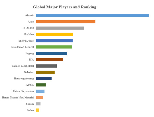
Selon QYResearch, les principaux fabricants mondiaux de Oxyde d'aluminium calciné comprennent Almatis, Alteo, CHALCO, Hindalco, Showa Denko, Sumitomo Chemical, Jingang, ICA, Nippon Light Metal, Nabaltec, etc. En 2023, les dix premiers acteurs mondiaux détenaient une part d'environ 48.0% en termes de chiffre d'affaires.
Figure 2. Classement et part de marché des 16 premiers acteurs mondiaux de Oxyde d'aluminium calciné (Le classement est basé sur le chiffre d'affaires de 2023, continuellement mis à jour)
The market for calcined aluminum oxide, also known as alumina, is influenced by various factors that drive demand and supply dynamics within the industry. Here are some key drivers that impact the calcined aluminum oxide market:
1. Growing Demand in the Ceramics Industry: Calcined aluminum oxide is a crucial raw material in the ceramics industry, where it is used in the production of high-quality ceramics, refractories, and abrasives. The demand for calcined alumina in the ceramics sector is driven by infrastructure development, increased construction activities, and the growing need for advanced ceramic materials in various applications.
2. Increasing Demand in the Abrasives Industry: Calcined aluminum oxide is widely used as an abrasive material in applications such as grinding wheels, sandpaper, and polishing. The abrasives industry's growth, driven by diverse sectors like manufacturing, automotive, construction, and metalworking, contributes significantly to the demand for calcined alumina.
3. Growing Demand in Refractories: Calcined aluminum oxide plays a crucial role in the production of refractory materials used in high-temperature applications like steelmaking, glass production, and cement manufacturing. The demand for refractories in industries such as metallurgy and construction influences the market for calcined alumina.
4. Increasing Demand in the Electronics Industry: The electronics industry uses calcined aluminum oxide in various applications such as insulating components, electronic packaging, and substrates for semiconductor production. The growth of the electronics sector, including developments in semiconductors, LEDs, and electronic components, drives the demand for high-purity calcined alumina.
5. Automotive and Aerospace Applications: Calcined aluminum oxide is used in automotive and aerospace applications for components requiring high strength, wear resistance, and thermal stability. As these industries continue to innovate and demand high-performance materials, the need for calcined alumina as a key component in advanced materials grows.
6. Environmental Regulations and Sustainability: Increasing focus on environmental regulations and sustainability practices is driving the demand for eco-friendly materials in various industries. Calcined alumina produced using sustainable practices and meeting stringent environmental standards can attract environmentally conscious consumers and industries.
7. Research and Development: Advancements in manufacturing processes, product quality, and new applications for calcined aluminum oxide can drive market growth. Continuous research and development efforts to improve the properties and applications of calcined alumina can open up new market opportunities.
8. Global Economic Trends: Macroeconomic factors like industrial output, GDP growth, infrastructure development, and global trade impact the demand for calcined aluminum oxide. Market fluctuations, currency exchange rates, and geopolitical factors can also influence the market dynamics for calcined alumina.
À propos de QYResearch
QYResearch a été fondée en 2007 en Californie aux États-Unis. C'est une société de conseil et d'étude de marché de premier plan à l'échelle mondiale. Avec plus de 17 ans d'expérience et une équipe de recherche professionnelle dans différentes villes du monde, QYResearch se concentre sur le conseil en gestion, les services de base de données et de séminaires, le conseil en IPO, la recherche de la chaîne industrielle et la recherche personnalisée. Nous société a pour objectif d’aider nos clients à réussir en leur fournissant un modèle de revenus non linéaire. Nous sommes mondialement reconnus pour notre vaste portefeuille de services, notre bonne citoyenneté d'entreprise et notre fort engagement envers la durabilité. Jusqu'à présent, nous avons coopéré avec plus de 60 000 clients sur les cinq continents. Coopérons et bâtissons ensemble un avenir prometteur et meilleur.
QYResearch est une société de conseil de grande envergure de renommée mondiale. Elle couvre divers segments de marché de la chaîne industrielle de haute technologie, notamment la chaîne industrielle des semi-conducteurs (équipements et pièces de semi-conducteurs, matériaux semi-conducteurs, circuits intégrés, fonderie, emballage et test, dispositifs discrets, capteurs, dispositifs optoélectroniques), la chaîne industrielle photovoltaïque (équipements, cellules, modules, supports de matériaux auxiliaires, onduleurs, terminaux de centrales électriques), la chaîne industrielle des véhicules électriques à énergie nouvelle (batteries et matériaux, pièces automobiles, batteries, moteurs, commande électronique, semi-conducteurs automobiles, etc.), la chaîne industrielle des communications (équipements de système de communication, équipements terminaux, composants électroniques, frontaux RF, modules optiques, 4G/5G/6G, large bande, IoT, économie numérique, IA), la chaîne industrielle des matériaux avancés (matériaux métalliques, polymères, céramiques, nano matériaux, etc.), la chaîne industrielle de fabrication de machines (machines-outils CNC, machines de construction, machines électriques, automatisation 3C, robots industriels, lasers, contrôle industriel, drones), l'alimentation, les boissons et les produits pharmaceutiques, l'équipement médical, l'agriculture, etc.
0 notes
Text
Why use ceramics for circuit boards?
Ceramic circuit boards are actually made of electronic ceramics material and can be made into various shapes. Among them, the ceramic circuit board has the most outstanding characteristics of high temperature resistance and high electrical insulation performance, and has the advantages of low dielectric constant and dielectric loss, high thermal conductivity, good chemical stability, and similar thermal expansion coefficient of the component, and Ceramic printed circuit boards are produced using LAM technology, a laser rapid activation metallization technology. Used in LED field, high power semiconductor module, semiconductor cooler, electronic heater, power control circuit, power mixing circuit, intelligent power component, high frequency switching power supply, solid state relay, automotive electronics, communication, aerospace and military electronics Component.
Unlike traditional FR-4 (glass fiber) , ceramic materials have good high-frequency performance and electrical properties, and have high thermal conductivity, chemical stability and thermal stability. The ideal packaging material for a generation of large-scale integrated circuits and power electronics modules.
Main advantages:
1. Higher thermal conductivity
2. be assembled in high density
3. Good insulation
4. The solder ability of the substrate is good and the use temperature is high
5. More matching coefficient of thermal expansion
6. Low frequency loss
7. A harder, lower resistance metal film aluminum oxide ceramic circuit board
8. Free of organic constituent, resistant to cosmic rays, high reliability in aerospace and long service life
9. The copper layer does not contain an oxide layer and can be used for a long time in a reducing atmosphere.
If you want to know ceramic PCBs, please feel freely to contact Cynthia at [email protected]
0 notes
Text
Unlocking the Potential of Silicon Carbide Ceramics: A Revolution in Durability and Efficiency
In the realm of advanced ceramics, silicon carbide (SiC) emerges as a standout material that is forging pathways toward new levels of performance in various industries. Silicon carbide ceramics are renowned for their exceptional properties, which include extraordinary hardness, high thermal conductivity, excellent wear resistance, low thermal expansion, and outstanding chemical stability. These characteristics make SiC ceramics an incredibly valuable component in applications where conventional materials might falter under extreme conditions.
### What is Silicon Carbide Ceramic?
Silicon carbide, a compound of silicon and carbon with a chemical formula of SiC, is a synthetic material known for its hardness next only to diamonds. It is produced through the Acheson process – a technique involving the reduction of silica sand with carbon in an electric resistance furnace. The resulting non-oxide ceramic is a polymorphic material, with numerous crystalline forms that grant it a wide range of properties suitable for different applications. The primary forms of SiC ceramics include sintered SiC, reaction bonded SiC, and hot pressed SiC, each with its unique fabrication process and use-case scenarios.
### Exceptional Physical Properties
One of the most compelling advantages of SiC ceramics is their extraordinary hardness. With a Mohs scale rating close to diamonds, these ceramics can endure severe abrasion and maintain their shape and functionality, where metals or polymer components would wear down.
Their thermal conductivity is equally impressive, which makes them ideal for applications that demand rapid heat dissipation. This includes electronics, where SiC substrates can help to cool devices, and in braking systems of vehicles, where they manage the heat generated during operation.
Moreover, SiC ceramics boast a low thermal expansion, ensuring dimensional stability across a range of temperatures. This property is crucial in precision applications such as aerospace components, where materials cannot afford to alter in shape in response to changing temperatures.
### Superior Chemical Stability
In chemically aggressive environments, SiC ceramics hold their own, showing remarkable resistance to oxidation and corrosion. This resistance extends the lifespan of components made from SiC and reduces maintenance needs, translating to long-term cost savings.
### Industrial and Commercial Applications
The industrial applications of SiC ceramics are extensive and diverse. In the automotive industry, SiC ceramic components are employed in pumps, rotors, and other parts that encounter high wear conditions. The material's resistance to high temperatures and corrosive substances makes it ideal for these applications.
In energy sectors, particularly within nuclear power plants, SiC’s resilience to radiation and thermal shock makes it an excellent choice for cladding material and other structural components. SiC-based ceramics are also being utilized in the rapidly growing field of semiconductor electronics, especially in high-voltage, high-temperature devices such as diodes, transistors, and LED lights.
Aerospace is another sector where SiC ceramics have made significant inroads. Components such as turbine blades, vanes, and other engine parts benefit from the material's resistance to thermal shock and wear. The telecom industry has recognized the material's potential in mirror substrates for space telescopes and other precision optical components, given its low weight and high stiffness-to-weight ratio.
### Advancements in Manufacturing Processes
The continued development of SiC ceramic manufacturing processes is a testament to the growing demand for this innovative material. Techniques such as chemical vapor deposition (CVD), hot pressing, and liquid-phase sintering have evolved to create high-purity, dense SiC ceramics with tailored properties for specific applications.
### Environmental Impact and Sustainability
Silicon carbide ceramics also contribute to environmental sustainability by enhancing the energy efficiency of systems where they are integrated and by optimizing lifespan due to their durability. SiC-based power electronics, for instance, operate at higher temperatures with greater efficiency, reducing cooling requirements and, consequently, energy consumption. Furthermore, their longevity reduces the need for frequent replacement, leading to less material waste.
### The Future of SiC Ceramics
Innovation continues to drive the future of SiC ceramics, with research focusing on enhancing properties such as electrical conductivity and creating composites that integrate SiC with other materials to achieve even greater performance benchmarks.
Investments in the automotive and aerospace industries signal a significant trend towards the adoption of SiC ceramics, propelled by the push for higher performance and improved energy efficiency. As electric vehicles become more prevalent, SiC components in electric motors and power electronics are expected to become standard, further reinforcing the material's position in the market.
### Embracing the SiC Ceramic Revolution
Silicon carbide ceramics represent a significant advancement in material science, offering a combination of properties that can be finely tuned to meet the requirements of the most demanding applications. As industries continue to discover new uses for this versatile material, the development of SiC ceramics is bound to accelerate, pushing the boundaries of what is possible in terms of performance, efficiency, and durability.
Businesses and researchers that embrace the potential of SiC ceramics stand at the forefront of a technological revolution, ready to unlock new levels of innovation and efficiency. As we move into an era where material capabilities are critical to competitive advantage, silicon carbide ceramics are poised to play a pivotal role in shaping the future of technology and industrial advancement.
0 notes
Text
UV cure adhesive
**Title: Illuminating Innovation: Exploring the Advantages of UV Cure Adhesive**
**Introduction:**
In the realm of industrial adhesives, UV cure adhesive stands out as a beacon of innovation, offering unparalleled efficiency and performance. Utilizing ultraviolet light to initiate curing, UV cure adhesive has revolutionized bonding processes across various industries. From rapid curing times to exceptional bond strength, UV cure adhesive has become a cornerstone of modern manufacturing. In this article, we delve into the advantages and applications of UV cure adhesive, showcasing its transformative impact on production processes worldwide.
**Understanding UV Cure Adhesive:**
UV cure adhesive is a type of adhesive that cures rapidly when exposed to ultraviolet light. Comprising monomers, oligomers, photoinitiators, and additives, UV cure adhesive undergoes polymerization and crosslinking upon UV exposure, forming a strong bond between substrates. Unlike traditional adhesives that rely on heat or chemical reactions for curing, UV cure adhesive offers instant curing, significantly reducing assembly time and increasing productivity.
**Advantages of UV Cure Adhesive:**
1. **Speedy Curing:** One of the most notable advantages of UV cure adhesive is its rapid curing time. Within seconds or minutes of exposure to UV light, the adhesive undergoes polymerization, resulting in an instantaneous bond formation. This accelerated curing process enables manufacturers to streamline production and meet tight deadlines effectively.
2. **Exceptional Bond Strength:** Despite its fast curing time, UV cure adhesive delivers exceptional bond strength. The crosslinked polymer network created during curing ensures robust adhesion between substrates, resulting in durable and long-lasting bonds. Whether bonding plastics, metals, glass, or ceramics, UV cure adhesive provides reliable performance across a wide range of applications.
3. **Versatility and Compatibility:** UV cure adhesive exhibits versatility in terms of substrate compatibility and application methods. It can bond various materials, including transparent substrates, without discoloration or visible residue. Additionally, UV cure adhesive is compatible with automated dispensing systems, allowing for precise and uniform application in high-volume production environments.
4. **Environmental Benefits:** UV cure adhesive offers environmental advantages compared to traditional solvent-based adhesives. With no volatile organic compounds (VOCs) or hazardous emissions released during curing, UV cure adhesive supports sustainable manufacturing practices and contributes to a healthier work environment.
**Applications of UV Cure Adhesive:**
The versatility and performance of UV cure adhesive make it suitable for a wide range of applications across industries:
- **Electronics:** In the electronics industry, UV cure adhesive is used for bonding components such as circuit boards, display screens, and semiconductors. Its fast curing time and excellent electrical insulation properties make it ideal for high-precision assembly processes.
- **Medical Devices:** UV cure adhesive finds extensive use in the medical sector for bonding medical devices and equipment. From surgical instruments to wearable sensors, UV cure adhesive provides biocompatibility, sterilization resistance, and precise bonding, meeting the stringent requirements of healthcare applications.
- **Automotive:** Automotive manufacturers utilize UV cure adhesive for bonding interior and exterior components, including trim panels, headlights, and automotive glass. Its ability to withstand temperature fluctuations, vibrations, and harsh environmental conditions ensures reliable performance in automotive assemblies.
- **Optoelectronics:** In optoelectronic applications such as LED lighting and display technology, UV cure adhesive is used for encapsulation, lens attachment, and bonding. Its optical clarity, UV stability, and moisture resistance contribute to the performance and longevity of optoelectronic devices.
**Conclusion:**
In conclusion, UV cure adhesive represents a significant advancement in bonding technology, offering speed, strength, and versatility unmatched by traditional adhesives. Its ability to cure rapidly upon exposure to UV light has revolutionized manufacturing processes across industries, enabling faster production cycles and superior bond performance. As the demand for efficient and sustainable adhesive solutions continues to grow, UV cure adhesive stands poised to play a pivotal role in shaping the future of industrial manufacturing. With its proven benefits and diverse applications, UV cure adhesive illuminates a path toward enhanced productivity, reliability, and innovation in the world of adhesives. Visit more: https://www.uvcureadhesive.com/
1 note
·
View note
Last Seen Blogs

industrialmanufacturingamerica
Best Industrial Manufacturing America

food-in-the-morning
Breakfast
industrialmanufacturingamerica
Best Industrial Manufacturing America
industrialmanufacturingamerica
Best Industrial Manufacturing America

our-quz
She's not Uquiz..she's Ourquiz