#metal clad pcb
Text
PCB Manufacturing in Toronto: Expertise, Services, and Local Industry Insights
Discover PCB manufacturing in Toronto, a hub of innovation and quality in electronic manufacturing services. Learn about the specialized capabilities, technological advancements, and diverse offerings of PCB manufacturers Toronto. Explore how local expertise and cutting-edge facilities contribute to producing high-quality printed circuit boards for various industries and applications worldwide. For more details visit our website www.crimpcircuits.com
#pcb manufacturing toronto#printed circuit board design#metal clad pcb#printed circuits#rigid flex pcb#full turnkey pcb services#turnkey pcb services#pcb parts#eagle software#pcb designing#flexible pcb#pcb assembly#printed circuit board manufacturers#pcb manufacturers in canada#circuit board manufacturers in canada#pcb quote#pcb prototype services in canada
2 notes
·
View notes
Text

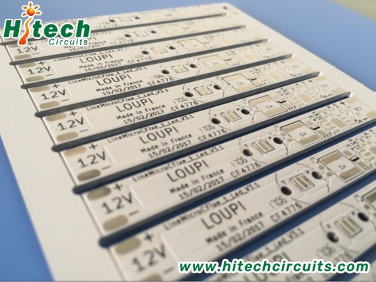
Heavy Copper PCB
Heavy copper pcb manufacturering up to 26 OZ
Hitech is a professional heavy copper pcb, thick copper pcb board manufacturer, PCB power supplier from China, we have been associated with heavy copper pcb plating since 2000 and we have won good reputation in this industry. If you have customized heavy copper pcb needs, please don’t heisitate to conatct [email protected] .
Demand for heavy copper PCB in Electric automotive, Power charge, voltage transformer, Charging station, industrial controls, and military is growing very fast. More than 80% of the existing printed wiring board manufacturing is limited or not capable of producing reliable heavy copper printed circuit boards.
Hitech thick copper board technology offers the possibility to implement complex switches in limited space in combination with circuitry for high current levels. Multi-layer PCB has reliable processes to produce copper layer thicknesses up to 26 Oz .
Hitech heavy copper PCB normally used for high power rectifiers, Power charge, Transformaer, Charging station, computer, military, electric vehicle charging, power grid switching system, etc

What is heavy copper PCB board
Heavy copper PCB boards ( also being called thick copper board, power board etc ) are usually bonded with a layer of copper foil on a glass epoxy substrate. The thickness of copper foil is usually 18μm, 35μm, 55μm and 70μm. The most commonly used copper foil thickness is 35μm. The thickness of copper foil used in China is generally 35-50μm, and there are also thinner ones such as 10μm and 18μm; and thicker ones such as 70μm. The thickness of the composite copper foil on a substrate with a thickness of 1-3mm is about 35μm; the thickness of the composite copper foil on a substrate with a thickness of less than 1mm is about 18μm, and the thickness of a composite copper foil on a substrate with a thickness of more than 5mm is about 55μm. If the thickness of the copper foil on the PCB is 35μm and the printed line width is 1mm, then for every 10mm length, its resistance value is about 5mΩ, and its inductance is about 4nH. When the di/dt of the digital integrated circuit chip on the PCB is 6mA/ns and the working current is 30mA, the resistance and inductance contained in each 10mm printed line are used to estimate the noise voltage generated by each part of the circuit to be 0.15. mV and 24mV.

Advantages of heavy copper PCB board
Heavy copper plate has the characteristics of carrying large current, reducing thermal strain, and good heat dissipation.
1. The heavy copper circuit board can carry large current
In the case of a certain line width, increasing the copper thickness is equivalent to increasing the cross-sectional area of the circuit, which can carry a larger current, so it has the characteristic of carrying a large current.
2. Heavy copper circuit boards reduce thermal strain
Copper foil has a small electrical conductivity (also called electrical resistivity ), the temperature rise is small when a large current is passed, so it can reduce the amount of heat and thereby reduce the thermal strain.
Metal “conductors” are divided into: ” silver→copper→gold→aluminum→tungsten→nickel→iron ” according to conductivity.
3. The heavy copper circuit board has good heat dissipation
Copper foil has high thermal conductivity (thermal conductivity 401W/mK), which can play an important role in improving heat dissipation performance, so it has good heat dissipation;
Thermal conductivity refers to the heat transfer through an area of 1 square meter within 1H for a 1 meter thick material with a temperature difference of 1°C on both sides under stable heat transfer conditions, measured by W/m·K.
Heavy copper plate has the characteristics of carrying large current, reducing thermal strain, and good heat dissipation.
Disadvantages of heavy copper PCB board
The outer copper-clad plane must be separated by the surface components and signal lines. If there is a poorly grounded copper foil (especially the thin and long copper), it will become an antenna and cause EMI problems.
If the pins of electronic components are fully connected with copper, it will cause the heat to dissipate too fast, and it will be difficult to desolder and rework soldering. The copper-clad plane of the outer layer must be well grounded, and more vias need to be punched to connect to the main ground plane. If more vias are punched, it will inevitably affect the wiring channels, unless buried blind vias are used.

Applications of heavy copper PCB board
The application field and demand for thick copper plates have been rapidly expanded in recent years, and it has become a “hot” PCB variety with good market development prospects.
The vast majority of heavy copper PCBs are high-current substrates (current x voltage = power). The main application areas of high-current PCBs are two major areas: power modules and automotive electronic components. Some of its main terminal electronic product fields are the same as conventional PCBs (such as portable electronic products, network products, base station equipment, etc.), and some are different from conventional PCB fields, such as automobiles, industrial controls, and power modules.
High-current PCBs are different from conventional PCBs in terms of efficacy. The main function of a conventional PCB is to form a wire for transmitting information. The high-current PCB has a large current through it, and the main function of the substrate carrying the power device is to protect the current carrying capacity and stabilize the power supply. The development trend of such high-current PCB is to carry larger currents, and the heat emitted by larger devices needs to be dissipated. Therefore, the large currents passing through them are getting larger and larger, and the thickness of all the copper foils of the PCBs is getting thicker and thicker. The 6 oz copper thickness of the high-current PCBs manufactured now has become normal;
The application areas of heavy copper circuit boards include: mobile phones, microwaves, aerospace, satellite communications, network base stations, hybrid integrated circuits, power supply high-power circuits and other high-tech fields.
#heavy copper pcb#pcb#pcb assembly#pcb designer#pcb layout#pcb manufacturing#pcb production#pcb supplier
4 notes
·
View notes
Text
Printed Circuit Board (PCB): The Backbone of Modern Electronics
A Printed Circuit Board (PCB) is an essential component in nearly all electronic devices. These boards are designed to mechanically support and electrically connect various electronic components using conductive pathways. The significance of PCBs in today’s technological landscape cannot be overstated, as they form the foundation upon which most modern electronics are built. Whether it's a smartphone, computer, or even complex industrial equipment, the PCB plays a crucial role in their functionality.
Structure and Components of a PCB
At its core, a PCB is made up of a non-conductive substrate material, typically fiberglass or composite epoxy, with conductive copper traces embedded on it. These traces form electrical circuits that allow components such as resistors, capacitors, transistors, and integrated circuits to communicate and work together. The components are mounted onto the board through a process called soldering, where a metallic substance binds them to the copper pads, ensuring strong electrical connections.
There are several layers in a typical PCB:
1. Substrate Layer: The base material, often fiberglass, provides rigidity and insulation.
2. Copper Layer: A thin copper foil is laminated onto the substrate, forming the conductive pathways.
3. Solder Mask Layer: This is a protective layer that covers the copper traces, preventing short circuits and oxidation.
4. Silkscreen Layer: Used for printing labels and markings, this layer helps technicians and engineers identify components on the board.
PCBs can range from simple single-layer boards to more complex multi-layer boards. In advanced applications, multi-layer boards are used, where multiple copper layers are sandwiched together with insulating layers between them. This allows for higher component density and more complex circuitry in a compact form factor.
Types of Printed Circuit Boards
PCBs come in several different types based on the complexity of the design and the needs of the application:
1. Single-Sided PCB: The simplest form, with components and copper traces on one side of the substrate.
2. Double-Sided PCB: These boards have components and copper traces on both sides of the substrate, offering more flexibility for routing electrical connections.
3. Multi-Layer PCB: As the name suggests, these boards have multiple layers of copper traces, making them ideal for complex and high-performance applications.
4. Rigid PCB: These are made from solid, inflexible materials, commonly used in devices where the board must maintain a specific shape.
5. Flexible PCB: These boards are made from flexible materials and can bend, fold, or twist. They are often used in compact devices where space is limited.
6. Rigid-Flex PCB: A hybrid of rigid and flexible PCBs, these are used in complex devices that require both flexibility and stability in specific areas.
Manufacturing Process
The manufacturing of a PCB involves several precise steps to ensure quality and reliability:
1. Design: The process begins with creating a design using PCB design software. This includes defining the layout, trace routing, and component placement.
2. Printing the Design: Once the design is finalized, it is printed onto the copper-clad substrate using a photomask or a direct laser printing method.
3. Etching: Any excess copper is removed from the board, leaving only the desired copper traces.
4. Drilling and Plating: Holes are drilled where components will be placed, and conductive materials are plated inside these holes to establish connections between layers in multi-layer boards.
5. Solder Mask Application: A solder mask is applied to protect the copper traces and prevent short circuits.
6. Silkscreen Printing: Component labels and identification markers are printed onto the board.
7. Testing and Quality Control: The finished PCB undergoes rigorous testing to ensure there are no defects in the circuitry or connections.
Applications of PCBs
PCBs are found in a vast array of electronic devices and systems. Some of the key application areas include:
Consumer Electronics: Smartphones, tablets, computers, and home appliances rely heavily on PCBs for their operation.
Automotive Industry: Modern vehicles contain numerous electronic systems, from engine control units to infotainment systems, all powered by PCBs.
Medical Devices: Precision medical equipment like diagnostic machines and wearable health devices depend on reliable PCBs for accurate functionality.
Telecommunications: Communication devices, including routers, switches, and mobile towers, are equipped with PCBs that handle data processing and signal transmission.
Aerospace and Defense: In high-stakes industries like aerospace and defense, robust PCBs are required for mission-critical systems, including avionics and radar equipment.
Future Trends in PCB Technology
As technology continues to evolve, so too does the development of PCBs. Advances in materials science, miniaturization, and automation are paving the way for even smaller and more powerful PCBs. Innovations such as flexible hybrid electronics (FHE), 3D-printed circuits, and high-speed PCB designs are expected to revolutionize industries by enabling more compact, lightweight, and efficient electronic devices.
Moreover, with the rise of the Internet of Things (IoT) and 5G technology, the demand for high-performance PCBs capable of handling greater data transmission speeds and power efficiency is surging. This trend will likely lead to more widespread use of multi-layer and flexible PCBs in upcoming technological advancements.
Conclusion
The printed circuit board is undeniably one of the most vital components in modern electronics. Its evolution has allowed for remarkable advancements in technology, from the devices we use daily to the complex systems that run industries. As innovations in materials and design continue, PCBs will remain at the forefront of the ever-expanding world of electronics, enabling new possibilities and driving the next wave of technological breakthroughs.
1 note
·
View note
Text

Copper core PCB is a copper substrate + Insulated layer + copper circuits layer PCB,also, it is called copper substrate pcb, copper based pcb, copper clad pcb. https://www.htmpcb.com/metal-core-pcb-c-10.html
PCB PCB Manufacturer PCB Manufacturing Electronics
0 notes
Text

4 Advantages and 8 Applications of Aluminum PCB
Stack-layer of Singe Aluminum PCB
It features a thermal clad layer that dissipates heat in a highly efficient manner, while cooling components and increasing the overall performance of the products.
Advantages of Aluminum PCB
1. Environmentally Friendly: Aluminum is non-toxic and recyclable. Manufacturing with aluminum is also conducive to conserving energy due to its ease of assembly. For printed circuit board suppliers, using this metal helps maintain the health of our planet.
2. Heat dissipation: High temperatures can cause severe damage to electronics, so it is wise to use a material that can help dissipate heat. Aluminum can actually transfer heat away from vital components, thus minimizing the harmful effect it could have on the circuit board.
3. Higher durability: Aluminum provides strength and durability to a product that ceramic or fiberglass bases cannot provides. Aluminum is a sturdy base material that can reduce accidental breakage during manufacturing, handling, and everyday use.
4. Lightweight: For its incredible durability, aluminum is a surprisingly lightweight metal. Aluminum adds strength and resilience without adding on any additional weight.
8 Applications of Aluminum PCB
1. Audio device: Input, output amplifier, balanced amplifier, audio amplifier, pre-amplifier, power amplifier.
2. Power Supply: Switching regulator, DC / AC converter, SW regulator, etc.
3. Communication electronic equipment: High-frequency amplifier, filtering appliances, transmitter circuit
4. Office automation equipment: Motor drive, etc.
5. Automobile: Electronic regulator, ignition, power supply controller, etc.
6. Computer: CPU board, floppy disk drive, power supply devices, etc.
7. Power Modules: Inverter, solid state relays, rectifier bridges.
8. Lamps and lighting: As the advocated promotion of energy-saving lamps, a variety of colorful energy-saving LED lights are well received by the market, and aluminum pcb used in LED lights also begin large-scale applications.
0 notes
Text
Dupont De Nemours Inc Innovates with Pyralux ML Laminates for PCBs, Driving Future Growth $DD #NYSE
Cost Reduction Initiatives and Product Innovation Position Dupont De Nemours Inc for Success Dupont De Nemours Inc, a leading innovation and technology company, has recently introduced its latest Pyralux ML double-sided metal-alloy-clad laminates to its Pyralux lineup for flexible and rigid-flex printed circuit boards (PCBs). These laminates have high thermal management properties, making them suitable for extreme environments. This new addition to Dupont's product portfolio is expected to have a positive impact on the company's performanc
0 notes
Text
What is aluminium PCB board ?

Aluminium PCB board, also named Aluminium based PCB, metal clad (MCPCB) PCB, insulated metal substrate(IMS or IMPCB) PCB, thermally conductive PCBs, etc. Aluminum printed circuit board ( PCB ) is a unique metal-based copper clad laminate with good thermal conductivity, electrical insulation performance and mechanical processing performance. It is composed of copper foil, thermally conductive insulating layer and metal substrate. It is generally including single layer, double layer and multi layer aluminum pcb board.
1 note
·
View note
Video
undefined
tumblr
Need PCBs for your security, industrial control, or automotive electronics?
PTH of PCB manufacturig Drilling is to drill the required vias in the copper clad PCB board. PCB vias are divided into plated holes ( PTH ) and non-plated holes (NPTH) according to whether they are metallized. According to the process, it is divided into blind holes of the PCB, buried holes and through holes. Vias mainly provide electrical connections and are used for fixing or positioning devices. Website: www.camtechcircuits.com [email protected]
0 notes
Text
Exploring the Advantages of Rocket-PCB’s Aluminum PCB

Rocket-PCB takes pride in offering cutting-edge Aluminum PCB solutions that leverage the advantages of aluminum-based copper-clad laminate technology. These metal PCBs combine a copper circuit layer, a dielectric insulation layer, and a metal substrate, creating a high-performance and versatile platform for various applications. In this article, we will delve into the features and benefits of Rocket-PCB’s Aluminum PCBs, highlighting their superiority over traditional FR-4 boards.
Aluminum-Based Copper-Clad Laminate Technology
The foundation of Rocket-PCB’s Aluminum PCB lies in the innovative aluminum-based copper-clad laminate technology. This unique material composition comprises three essential layers: circuit layer, dielectric layer, and base layer.
Circuit Layer: The circuit layer in an Aluminum PCB is akin to standard PCB copper clad laminates, with copper foil thickness ranging from 1oz to 10oz. This layer allows for efficient signal transmission and supports higher current carrying capacity.
Dielectric Layer: The dielectric layer is a crucial component in Aluminum PCBs, providing low thermal resistance insulation. With a thickness ranging from 0.003" to 0.006" inch, this layer is the core technology behind Rocket-PCB’s Aluminum PCBs and has received UL certification, ensuring reliability and safety.
Base Layer: Serving as the foundation, the base layer consists of a metal substrate, commonly aluminum or copper. This metal substrate distinguishes Aluminum PCBs from traditional epoxy glass cloth laminates and significantly contributes to their superior performance.
Advantages of Aluminum Base PCBs
Rocket-PCB’s Aluminum Base PCBs possess a range of advantages over traditional FR-4 boards, making them a preferred choice for various applications.
Thermal Conductivity: Aluminum is known for its excellent thermal conductivity, which is vital for dissipating heat generated by electronic components. Compared to FR-4 boards, Aluminum PCBs offer significantly higher thermal conductivity, exceeding 2.0 kW/(m.h.℃). This property ensures efficient heat dissipation and enhances the reliability and lifespan of electronic devices.
Electrical Insulation: Despite its metal composition, Aluminum PCBs maintain excellent electrical insulation properties. This characteristic is crucial for preventing short circuits and ensuring the proper functioning of complex electronic systems.
Mechanical Processing Performance: The low alloy Al-Mg-Si system high plastic alloy plate used in Rocket-PCB’s Aluminum PCBs contributes to their exceptional mechanical processing performance. This allows for ease of fabrication, making it easier to create intricate designs and meeting specific project requirements.
Higher Current Carrying Capacity: Thanks to the excellent thermal conductivity and unique material composition, Aluminum PCBs can carry higher currents compared to traditional FR-4 boards. This capability is essential for power-intensive applications where efficiency and reliability are critical.
High Withstand Voltage: Rocket-PCB’s Aluminum PCBs can withstand voltages of up to 4500V, providing an added level of safety and stability for high-voltage applications.
Rocket-PCB’s Aluminum PCBs stand at the forefront of advanced PCB solutions, harnessing the power of aluminum-based copper-clad laminate technology. With their superior thermal conductivity, electrical insulation, mechanical processing performance, and higher current carrying capacity, these PCBs cater to a wide range of applications, including power electronics, LED lighting, automotive systems, and more. By choosing Rocket-PCB’s Aluminum PCBs, customers can be assured of high-quality, reliable, and efficient electronic solutions for their projects.
0 notes
Text
Leading Circuit Board Manufacturers in Canada: Precision and Innovation
Canada is home to a growing number of circuit board manufacturers in canada offering high-quality PCB solutions for a wide range of industries. These manufacturers specialize in producing advanced printed circuit boards (PCBs), including rigid, flexible, and metal-clad designs, serving sectors such as telecommunications, automotive, aerospace, and medical devices. Canadian PCB manufacturers are known for their commitment to precision, quality, and innovation, often providing customized solutions to meet specific client needs. With state-of-the-art facilities and a focus on sustainability, these companies help drive technological advancements while ensuring reliable performance in demanding environments. For more details visit our website www.crimpcircuits.com
#pcb manufacturing toronto#printed circuit board design#metal clad pcb#printed circuits#rigid flex pcb#full turnkey pcb services#turnkey pcb services#pcb parts#eagle software#pcb designing#flexible pcb#pcb assembly#printed circuit board manufacturers#pcb manufacturers in canada#circuit board manufacturers in canada#pcb quote#pcb prototype services in canada
0 notes
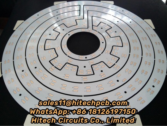
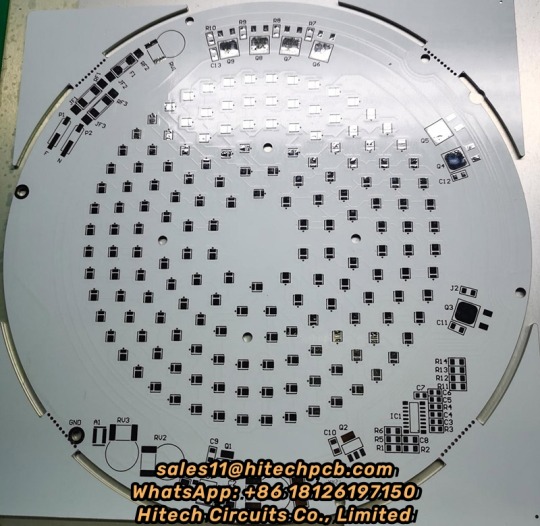
Text

Aluminium PCB
Aluminium PCB are metal-based, copper-clad laminates with a good heat dissipation function. Usually, Aluminium PCB is refer to LED PCB board, which is the most important part of LED display and lighting products, etc.
Hitech Circuits Co., Limited is a professional aluminum pcb board, LED PCB manufacturer in China. Through 10 years of aluminum pcb board designing and manufacturing experience, Hitech are able to provide high quality and cost effective single layer, double layer and multi layer aluminum pcb boards to global customers. For any of your requirements regarding aluminum pcb board, please don’t hesitate to contact [email protected]
#Aluminium PCB#aluminum pcb#pcb assembly#pcb#engineering#technology#pcba#pcb manufacturer#pcbassembly#pcb design#hardware
5 notes
·
View notes
Text

Acme Circuits is reliable MCPCB manufacturer and exporter from India. We manufacture aluminum-clad PCB, metal core PCB, and metal-clad PCB using quality-tested material and modern technology
#Printed Circuit Board Manufacturers#pcb manufacturing#printed circuit board assembly#circuit board manufacturing#pcb board manufacturer#high frequency pcb manufacturing#printed circuit board manufacturers near me#pcb manufacturer#pcb supplier#pcb assembly services#pcb assembly manufacturer#electronic cable assembly#electronic contract services#pcb exporters#printed circuit board manufacturer in india#pcb manufacturing companies in india
1 note
·
View note
Text

Copper core PCB is a copper substrate + Insulated layer + copper circuits layer PCB,also, it is called copper substrate pcb, copper based pcb, copper clad pcb. For more information, you can visit our website https://www.htmpcb.com/metal-core-pcb-c-10.html
0 notes
Text
Aluminium PCB
1. What’s Aluminium LED PCB?
Aluminum LED PCB substrate is a metal - based copper-clad sheet with good heat dissipation. A single panel is generally composed of three layers of structure, namely the circuit layer (copper foil), insulation layer and metal base layer. It is commonly found in LED lighting products. There are two sides, the white side is used to weld the LED pins, and the other side is the natural color of aluminum, which is usually coated with heat-conducting gel and then in contact with the heat-conducting part. Among all metal core PCBS, Aluminum LED PCB is the most common type. The base material consists of an aluminum core and standard FR4. It features a thermal cladding that dissipates heat in an efficient manner while cooling components and improving the overall performance of the product. Currently, aluminum-backed PCBS are considered solutions for high power and tight tolerance applications.
2. Aluminum LED PCB with Copper Layer, Dielectric Layer & Aluminum Layer
Aluminum LED PCB has a similar layout to any other printed circuit boards with copper layer(s), solder mask layer(s) and silkscreen(s). Instead of having a fiberglass or plastic substrate, Aluminum LED PCB is made from metal core substrate, which consists of copper layer, dielectric layer and aluminum layer. This substrate is called as Aluminum based copper clad laminate (CCL). The glass reinforced and ceramic filled dielectric layer in-between copper layer and aluminum layer is very thin, but plays a very important role of electric insulation and thermal conductivity (because of minimum thermal resistance) from copper layer to aluminum base. The copper is etched into conductors and metal base is to withdraw thermal (/heat). The superior heat transfer capacity of Aluminum-based PCB helps cooling components while eliminating problems associated with managing fragile ceramics.
3. Thermal conductivity of Aluminium LED PCB
The general thermal conductivity of Aluminum LED PCB is 0.3, 0.6, 1.0, 1.5, 2.0, 3.0, 5.0, 122W/m.k, etc., among which 0.3-1.0w /m.k is the general conductive Aluminum LED PCB, 1.5W/m.k is the middle conductive Aluminum LED PCB, 2.0-3.0w /m.k is the high conductive Aluminum LED PCB. 5.0W/m.k is thin abasal substrate, and 122W/m.k is ultra-high conductivity Aluminum LED PCB, also known as ALC Aluminum LED PCB.
At present, the common Aluminum LED PCB on the market has a thermal conductivity of 1.0, 1.5, 2.0W/m.k high conductivity type Aluminium LED, wherein the thermal conductivity of 1.0W/m.k Aluminum LED PCB is called general Aluminum LED PCB, its insulation layer is composed of epoxy glass cloth bonded sheet; Aluminum LED PCB with thermal conductivity of 1.5W/m.k is called high heat dissipation Aluminum LED PCB, and its insulation layer is composed of epoxy resin or other resins with high thermal conductivity; The Aluminum LED PCB with a thermal conductivity of 2.0W/m.k is called the Aluminum LED PCB for high-frequency circuit, and the insulating layer is composed of polyolefin resin or Polyimide resin glass cloth bonded sheet. The thermal conductivity of Aluminum LED PCB varies according to the copper layer in the circuit. Different processes produce different levels of thermal conductivity.
We currently support Aluminum based CCLs from Ventec, GDM and BoYu with thermal conductivity from 1.0 ~ 7 W/m•K. The Aluminum LED PCB prices of Ventec is much higher than that with GDM and BOYU since material cost, and the prices of high thermal conductivity is higher than low thermal conductivity. Hitechpcb provides a wide range of electrical and thermally conductive interface pads, thermally conductive gap filler, thermal phase change materials and thermally conductive electrically insulating materials, as well as specialized equipment for high volume Aluminum LED PCB manufacturing. Choosing Hitech Circuits PCB as your Aluminum LED PCB supplier, just send your Gerber files and fabrication notes to us, we will deliver qualitied PCB boards to you on time.
4. Dielectric Constant of Aluminium LED PCB
The dielectric constant of Aluminum LED PCB substrate is a special detection method for Aluminum LED PCB. It is a variable Q value series resonance method through the measurement of dielectric constant and dielectric loss factor. The sample and tuning capacitor are connected in series to the high frequency circuit to measure the series circuit The principle of Q value.
The performance of Aluminum LED PCB includes requirements such as peel strength, surface resistivity, minimum breakdown voltage, dielectric constant, flammability and thermal resistance.
5. Aluminum LED PCB with White Solder Mask
The retail price of Aluminum LED lights has dropped dramatically in recent years, while the energy efficiency and brightness of LED lights have improved. These technological advances have led some to predict annual growth of 45% over the next five years. With the development of the LED industry, the demand for LED PCBS and solder masks is also increasing. Solder shield is a protective coating applied to exposed printed circuit boards. The exposed PCB board is covered with a mask to prevent accidental solder bridging during PCB assembly and to protect the PCB from the environment. Solder masks are traditionally green, and are expected to withstand the high temperatures that occur in reflow soldering, as different colors such as blue, red, or black will occasionally appear. Increased production of Hitch Aluminum LED PCB requires increased whiteness and color stability of the mask. Aluminum LED PCB commonly used LPI welding color is white and black, of which white welding color is the most commonly used to achieve high brightness and perfect light reflection. White Aluminum LED PCB ensures no darkening and will not affect the color temperature of LED smd. At the same time, it also helps to increase the life of LED applications. Looking for reliable Aluminum LED PCB suppliers, Hitech is a good choice.
6. Classification of Aluminum LED PCB Substrate
Aluminum LED PCB-based copper clad plates are divided into three categories:
The first is the universal aluminum-based copper clad plate, the insulation layer is composed of epoxy glass cloth bonded sheet;
The second is the high heat dissipation aluminum-based copper-clad plate, the insulation layer is composed of high thermal conductivity epoxy resin or other resins;
Third, high frequency circuit aluminum base copper plate, insulation layer by polyolefin resin or Polyimide resin glass cloth bonded sheet.
The biggest difference between aluminum clad copper plate and conventional FR-4 clad copper plate is heat dissipation. Compared with 1.5mm thickness of FR-4 clad copper plate and aluminum clad copper plate, the former thermal resistance of 20 ~ 22 ℃, the latter thermal resistance of 1.0 ~ 2.0℃, the latter is much smaller.
7. Aluminum LED PCB Performance:
(1) Heat dissipation
Many double panel, multi - layer plate high density, power, heat distribution is difficult. Conventional printed board substrates such as FR4, CEM3 are bad conductors of heat, insulation between layers, heat does not escape. Local heating of electronic equipment is not excluded, leading to high temperature failure of electronic components, and Aluminum LED PCB can solve this problem of heat dissipation.
(2) Thermal Expansibility
Thermal expansion and cold contraction is the common nature of substances, and the coefficient of thermal expansion of different substances is different. Aluminum based printed board can effectively solve the problem of heat dissipation, so that the printed board components of different substances on the thermal expansion and contraction problem, improve the durability and reliability of the whole machine and electronic equipment. Especially solve SMT (surface mount technology) thermal expansion and shrinkage problems.
(3) Dimensional stability
Aluminum-based printed boards are obviously much more stable in size than those made of insulating materials. Aluminum base printed board, aluminum sandwich board, heating from 30℃ to 140~150℃, the size change is 2.5~3.0%.
(4) Other reasons
Aluminum based printed board, with shielding effect; Instead of brittle ceramic substrate; Safe use of surface mounting technology; Reducing the real effective area of the printed board; Instead of radiator and other components, improve the heat resistance and physical properties of products; Reduce production costs and labor.
8. Why choose Aluminum LED PCB from Hitechpcb? What are the advantages of Aluminum LED PCB?
(1) Good heat dissipation performance: Aluminum LED PCB can reduce the thermal resistance to the minimum, has a smaller thermal resistance, thermal expansion coefficient is closer to copper foil, so that Aluminum LED PCB has excellent thermal conductivity and heat dissipation performance, reduce the module operating temperature, prolong the service life.
High current load: Using the same thickness, the same line width, Aluminum LED PCB substrate can carry higher current.
(2) Good machinability: can replace ceramic substrate, better mechanical endurance. At the same time, high strength and toughness, can realize large area printed board manufacturing and component mounting.
(3) Good electromagnetic shielding: In order to ensure the performance of electronic circuits, some components of electronic products need to prevent electromagnetic radiation and interference. Aluminum LED PCB can act as a shield plate, play the role of shielding electromagnetic wave
(4) Environmental protection: The Aluminum LED PCB used in the raw material is non-toxic and can be recycled. Meet RoHs requirements.
(5)Light weight: Aluminum LED PCB has a surprisingly light weight with excellent strength and elasticity, which is very convenient.
Hitech Circuits can provide high quality and affordable Aluminum LED PCB products for you.
9. Technical requirements for Aluminum LED PCB
The main technical requirements are:
1. Dimensional requirements: including panel size and deviation, thickness and deviation, perpendicularity and warpage; Appearance, including cracks, scratches, burrs and delimitation, aluminum oxide film, etc.
2. Performance requirements, including peel strength, surface resistively, minimum breakdown voltage, dielectric constant, combustion and thermal resistance requirements.
10. Special test method for Aluminum-based copper clad plates
One is the measurement method of dielectric constant and dielectric loss factor. It is the series resonance method with variable Q value. The sample and tuned capacitor are connected to the high-frequency circuit in series to measure the Q value of the series circuit.
The other is the measurement method of thermal resistance, which is calculated by the ratio of temperature difference and heat conduction between different temperature measurement points.
11. The Aluminum LED PCB manufacturing process in Hitechpcba
(1)Substrate cutting
a. cutting process: material → cutting
b. Note: ① Check the size of the first piece; ② Pay attention to Aluminum surface scratching and copper surface scratching; ③ Pay attention to the layering of the board edge and the tip.
(2)Plate drilling
a, drilling process: pin → drilling → inspection plate
b, matters needing attention: ① check the number of drilling holes, the size of the empty chestnut chain; ② Check the plate burr, hole deviation; ③ Avoid scratching the substrate; ④ Check and replace the drill nozzle.
(3) Imaging transfer
a, graphic imaging process: grinding plate → film → exposure → development
b, precautions: ① Check whether there is an open circuit after development; ② Pay attention to the poor line caused by the board wipe; ③ There can be no air residual exposure to prevent poor exposure; ④ Whether there is deviation in developing counterpoint; ⑤ After exposure, the development should be done at rest for more than 15 minutes.
(4)Solder mask and Silkscreen process
a, kill row silk printing resistance welding, character process: screen printing → pre-baking → exposure → development → character
b, matters needing attention: ① Check whether there is foreign body on the board; ② Pay attention to the cleaning of the net board; ③ Pre-bake for more than 30 minutes after screen printing, to avoid bubbles in the line; ④ Pay attention to the thickness and uniformity of screen printing; ⑤ After the pre-baked plate to completely mutual cooling, avoid touching film or damage to the ink surface gloss.
(5)E-test or flying probe test
a, test process: line test → withstand voltage test
b, precautions: ① How to distinguish after the test how to store qualified and unqualified products.
(6)FQC, FQA, packaging, shipping
a. Process: FQC→FQA→ Packaging → shipping
b. Note: ① FQC should pay attention to the confirmation of the appearance of the finished Aluminum LED PCB in the process of eye inspection and make a reasonable distinction; ② FQA does spot check and verify the inspection standards of FQC; ③ We should confirm the number of packages to avoid mixed plates, wrong plates and package
12. Application of Aluminum LED PCB
1. Audio devices: input, output amplifier, balance amplifier, audio amplifier, preamplifier, power amplifier.
2. Power Supply: switching voltage regulator, DC/AC converter, SW voltage regulator, etc.
3. Communication electronic equipment: high frequency amplifier, filter, transmitter circuit
4. Office automation equipment: motor drive, etc
5. Automobile: electronic regulator, ignition device, power controller, etc.
6. Computer :CPU board, floppy disk drive, power equipment, etc.
7. Power module: converter, solid relay, rectifier bridge, etc
8. Lamps and lighting: A variety of colorful LED energy-saving lamps are well received by the market, and Aluminum LED PCB used in LED lights has also begun to be applied on a large scale.
13. Aluminum LED PCB Storage Conditions
Aluminum LED PCB are generally stored in a dark and dry environment. Most Aluminum LED tube lighting metal core pcb are prone to dampness, yellowing, and blackening. Generally, they should be used within 48 hours after opening the vacuum package.
14. Specification for the manufacture of Aluminum LED PCB
a. Aluminum LED PCB is often used in power devices, power density is high, so the copper foil is thicker. If copper foils over 3oz are used, the etching of thick copper foils requires engineered line width compensation, otherwise the line width will be out of tolerance after etching.
b. The aluminum base surface of aluminum substrate must be protected by protective film in advance during PCB processing, otherwise, some chemicals will etch the aluminum base surface, resulting in appearance damage. And the protective film is easy to be hurt, resulting in gaps, which requires the whole PCB processing process must be inserted.
c. The hardness of the milling cutter used by the glass fiber board gong board is relatively small, and the hardness of the milling cutter used by the aluminum substrate is large. In the process of manufacturing glass fiber board milling cutter speed, while the production of aluminum substrate is at least two thirds slower.
d, computer milling glass fiber board is just the use of the machine's own cooling system, but the processing of aluminum substrate must be in addition to alcohol heat dissipation for the gong head.
15. Aluminum LED PCB circuit fabrication
(1) Mechanical processing: Drilling of aluminum substrate can be done, but no burr is allowed on the edge of the inner hole after drilling, which will affect the pressure test. Milling the shape is very difficult. And punching shape, need to use advanced mold, mold production is very skilled, as one of the difficulties of aluminum substrate. After shape punching, the edge should be very neat, without any burr, and do not hurt the welding resistance layer on the edge of the plate. Usually the use of soldier die, hole from the line, shape from the aluminum surface, circuit board punching force is cut down, and so on are skills. After punching the shape, the warpage of the board should be less than 0.5%.
(2) The whole production process is not allowed to wipe the aluminum base surface: aluminum base touch, or by a certain chemical will produce surface discoloration, blackening, which is absolutely unacceptable, re-polishing aluminum base some customers do not receive, so the whole process does not touch the aluminum base surface is one of the difficulties in the production of aluminum base plate. Some enterprises use passivation process, some in hot air leveling (spray tin) before and after each pasted protective film.
(3) Over-high voltage test: the aluminum base board of the communication power supply shall be tested at 100% high voltage. Some customers require direct current or alternating current. The voltage shall be 1500V or 1600V, and the time shall be 5 seconds or 10 seconds. Dirt on the board, holes and aluminum edge burr, line saw tooth, damage to any little insulation layer will lead to high voltage test fire, leakage, breakdown. Pressure test board stratification, foaming, are rejected.
1 note
·
View note
Text
Best PCBA Manufacturing Equipment Services in India
PCB is a Printed Circuit Board. It's a significant electronic part, which is a help for electronic parts and a transporter for electrical associations between electronic parts. As it is created by printing the expected picture on the substrate, it is known as a "printed" circuit board. It's most usually produced utilizing copper-clad epoxy sap/glass material compound.
The PCB is frequently comprised of various layers with 4 and 6 being the most normally utilized, depending on the necessary number of sign layers.
At the point when countless PCBs must be made, odds are parts will not be physically bound manually. This is where proficient gathering houses like Seeed will step in, to assist with manufacturing both the uncovered sheets and collect every one of the parts onto the Printed Circuit Boards, or PCBs.
Best PCBA Manufacturing Equipment Services in India - Syrma SGS
Yet, have you at any point thought about how your makers can stick that monstrous number of small parts onto your PCBs? I have, yet that was until I needed to drive through passages of specialized language online about the apparatus that takes care of business. While there's nothing provocative about PCBA producing, understanding how the cerebrums of all hardware are made most certainly gives pleasure and a feeling of achievement. Heaps of thought go into each phase of the gathering system to convey an entirely working board. Furthermore, with the gadgets getting increasingly progressed, the hardware used to make PCBs are steadily improving and more energizing than at any other time.
Best PCBA Manufacturing Equipment Services in India - Syrma SGS
In PCB gathering, there are 4 primary phases of SMT, or Surface Mount Technology get together utilizing the reflow strategy, which are glue application, mechanized part situation, binding, and review. The essential gear expected for PCB gathering incorporates:
Bind Paste Printing machine
Bind Paste Inspection (SPI) machine
Stick Dispensing machine
Pick-and-Place machine
Reflow Soldering machine
Wave Soldering machine (for through-opening parts)
Programmed Optical Inspection (AOI) machine
In-Circuit Test (ICT) Fixture
Practical Validation Test (FVT) Fixture
Best PCBA Manufacturing Equipment Services in India - Syrma SGS
Bind Paste Printing Machine
The initial phase in PCB gathering is the use of bind glue onto the board. Bind glue is a dim shaded goo produced using a combination of minuscule particles of metal compounds; normally of tin, lead, and silver. Consider it a paste that will keep your finished board intact. Without it, parts wouldn't adhere to your uncovered board.
Patch glue (left), PCB stencil laser-cut openings (right)
Before the glue is applied, a PCB stencil is set over the board. A PCB stencil is a tempered steel sheet that has little laser-cut openings that permit patch glue to be applied exclusively to the region of the board where the parts contacts will ultimately sit on the completed PCB, for example, the SMD cushions.
During the use of patch glue, the PCB stencil and the PCB are gotten into a place in the mechanized glue printer. A wiper then, at that point, applies without lead weld glue on the cushions in exact sums. The machine then hauls a cutting edge across the stencil, to spread and store the glue equitably in the ideal regions. After the stencil is taken out, the patch glue will be precisely where we maintain that it should be (ideally).
Best PCBA Manufacturing Equipment Services in India - Syrma SGS
Weld Paste Inspection (SPI) machine
Various industry studies have brought up that up to 70% of SMD binding issues are followed back to inappropriate or inadequate patch glue printing. Thus, the subsequent stage is to check to assume that the binding glue is printed appropriately onto the board. While utilizing great bind glue printing strategies are in many cases enough for PCBs in low volumes, SPI ought to be thought about while producing higher volumes of PCB to stay away from high modification costs.
0 notes
Text
Types of Printed Circuit Boards
Printed circuit boards are the basic component of many electrical appliances from pager to radios and computer systems to radars, almost every electrical appliance has a printed circuit board in it. With the development in electronics printed circuit boards (PCB) are also getting modified.
PCB is composed of a substrate which has a slight copper or aluminum layer on it. This substrate is known as copper-clad laminate. Visit https://www.dkenterprise.ind.in/copper-clad-laminates.html to get more information about copper Clad Laminates.

There are many types of PCB's which have their own specific usage, manufacturing specifications and material types.
These Types of PCB Include
Single-Layer PCB:
Single layer PCB is coated with a copper clad laminate at a single side of reinforcing material. For coating, copper is commonly used as metal due to high conductivity and heat resistance. After coating with copper clad laminate solder mask and silk layer is applied to mark the different circuits present at the board.
In single-layer PCB's all the components and circuits are soldered at the one side of the board and these types of boards are easy to manufacture.
Double-Layer PCB:
Double layer PCB's have the copper clad laminate coating at both sides of the board. In this type of PCB, holes are drilled at the edges of the board to connect with other circuits. Double-layer PCB's has more complex functions as compared to single-layer PCB's and consume less space.
Multi-Layer PCB's:
These printed circuit boards are the combination of three or more than three PCB's combined with layers of copper clad laminates. In these boards, a specific type of glue is used to ensure their reliability against excess of heat. These boards can vary in size from four-layer to ten to twelve layers. These types of boards are used in satellites, supercomputers, and complex storage devices.
Rigid PCB's:
These are the PCB's manufactured with a rigid material coated with copper clad laminates to prevent twisting of the board. This type of PCB is considered as the most commonly used PCB. These types of PCBs are used mostly in the motherboard of computers. Rigid PCB's can vary in size from single-layer board to multi-layer board consisting of ten to twelve layers.
Flexible PCB's:
These boards are composed of flexible material coated with copper clad laminates and can be stretched. They also vary in size from single layer's PCB's to multi-layer PCB's. They manufacturing cost is high due to complex fabrication of circuits but they could be more beneficial because they can be folded so consume less space and can also be shockproof, waterproof and corrosion resistant.
Aluminum Based PCB's:
In these PCB's aluminum copper clad laminate is used as coating material. This type of PCB has many advantages over other PCB's which includes
Low Cost: Aluminum is the most abundant metal on earth surface so prices for metal are comparatively low.
Environment Friendly: Aluminum can be easily recycled and is nontoxic. Due to use of Aluminum assembly of different components at the board is also easy.
Heat Dissipation: These types of PCB's have good heat dissipation capacity because aluminum transfer heat slowly so heat is dispersed into the open air instead of other parts of board.
DK Enterprise is very trust able suppliers of aluminum based PCB's. You can get more information about aluminum copper clad laminate from DK Enterprise.
Except the above mentioned types of printed circuit boards, there are also some other types which include high frequency PCB's and flex rigid PCB's, but these types are not commonly used.
1 note
·
View note
Last Seen Blogs

robot-rarepairs-dotcom
Transformers kissing but uncommon

moom-ml
題名未設定

crhserenity
Chira Ruiz

junicult
jo 𝜗𝜚

aworldincolour1-blog
Untitled