#printed circuit board fabrication
Text
Affordable PCB Design Services for High-Quality Prototypes
Looking for affordable PCB design services without compromising on quality? Bay Area Circuits offers expert solutions for high-quality PCB prototypes that meet your specific needs. Whether you're developing a simple single-layer board or a complex multi-layer design, our experienced team ensures precision and efficiency in every project.
Our services extend beyond just design. We provide printed circuit board fabrication, delivering fast, reliable, and cost-effective solutions. With cutting-edge equipment and years of experience, we create prototypes that meet industry standards, ensuring your product performs optimally from the start.
We also offer advanced printed circuit board design software like InstantDFM to streamline your design process. This tool allows you to check for manufacturability, reduce errors, and optimize your design, saving you time and money. InstantDFM provides automated feedback and pricing within minutes, ensuring a smooth transition from design to production.
Choose Bay Area Circuits for affordable PCB design services and high-quality prototypes. With our expertise, you can bring your electronic products to market faster and with confidence. Contact us today! To know more, Visit - https://bayareacircuits.com/
0 notes
Text
What is a Printed Circuit Board?
Printed Circuit Boards are boards that connect various points together through lines and pads. They allow signals and power to connect between two separate physical devices. While the term “printed circuit board” is typically used, other terms to describe these include “printed wiring board” and “printed wiring card.”

#marketing#investing#finance#branding#pcb circuit#pcb#pc build#pcb assembly#flexible circuit board#pcb board fabrication#pcb circuit design#pcb circuit in Gujarat#pcb design company#Printed Circuit Boards
3 notes
·
View notes
Text
The Ultimate Guide of Mastering PCB Design Guidelines
Take considerable time to learn the fundamental PCB design rules and regulations in order to get the hang of printing circuit boards (PCBs) through artful designing. Proper and perfect PCB designing is key. In this article, we explore these tips.
What is a printed circuit board (PCB) Layout?
The design process of Printed Circuit Board (PCB) is one indispensable step to electronic devices manufacture. It describes the arranging and networking of the electronic elements on the printed board, made of the composite material (such as fiberglass or epoxy) in which the bulk of electrical components of the device is not conductive.

Adjustments are the process of placing components like resistors and capacitors according to the circuit schematics. The following step is the horizontal trace routing which involves creating electrical pathways, traces that connect components with the power and ground that is supplied according to the schematic. These traces are usually copper and they are written using either laser ablation or electromigration to get them to look like that. Through a circuit routing process the chosen signals as well as their integrity, reduce electrical noise, and maintain impedance control.
What are the fundamental PCB designing rules?
When designing a a printed circuit board design (PCB), there are several fundamental rules to follow to ensure a successful outcome:
Component Placement
Space that is employed in every add-on on the PCB is optimized by carefully selecting a place for each component as well as minimizing signal interference and improving the assembly procedure through hole components. Component placement orientation and density is a crucial factor as any interference presumed.
Trace Routing
Being the route of current (the electrical pathway), carefully link up components, as shown on the printed circuit board traces and schematic. Secure against any sign of line widths, space, and impedance for the sake of signal quality and suppression of electrical noise.
Signal Integrity
Keep signal quality respected by avoiding bends or corners in signal traces, which may be negligible in traces, high speed digital signals should not be exposed to noise sources. Wisely plan where to use your ground planes and routing layers to decrease the level of electromagnetic interference (EMI).
Power Distribution
Implement the reliable power movement mechanism along PCB for constant power supply. Use power supply that has their power plane and decoupling capacitors in the most appropriate positions to limit the voltage fluctuations and ensure that the components get clean power and no power circuit interference.
Thermal Management
Make temperature control a key consideration that will enable components to release heat efficiently. Discover the Power of Tremendous Transformation: The Progression from High School to College Insert various phases of the hot components apart and used thermal vias or heatsinks if temperature reaches high to avoid thermal demands.
Design for Manufacturability (DFM)
Develop the PCB design with manufacturability taken into account as it is around the minimum of trace widths/gap, the plating weight of copper, and the wave soldering mask clearance. Use accepted in the industry guidelines for designing so that the manufacturing processes may be started quickly and less expensively.
Testing and Prototyping
Pin down the vital test points and features allowing for ease of evaluations during the prototyping and manufacturing time. Make, install and configure critical signals for both testing and debugging purposes.
How does component placement affect signal routing and thermal management?
Components positioning is especially significant for signal routing and heat management inside the electronic circuit. Here's how:
Signal Routing:

Signal Integrity: The placement of component has a significant effect on the trace's length and impedance. Wider design space and manageable impedance paths provide capabilities of signal quality that are enabling in terms of minimalizing signal degradation, reflections and crosstalk.
High-Speed Signals: For very high-speed signals that are necessary in digital communications and RF circuits, component placement is especially significant for the reduction of distortion caused by transmission lines effects, and EMI.
Clock Distribution: With the clock synchronizing elements located near the devices they generate the outputs, the clock skew and jitter are minimized, making the concurrent operation perfectly accurate in various sections of the system.
Analog vs. Digital Components: Way of separating analog and digital components from each other makes it impossible for any digital circuit noise to be an interference to the sensitive analog signals.
Thermal Management:
Heat Dissipation: Components produce heat running their operations and the area of placement just determines how well this heat gets dissipated. Grouping high-power components into one area can result in hot spots because there is not enough airflow away from the group. If effective cooling is required then distribution of load over several areas will also achieve good airflow.
Proximity to Heat Sources: Elements placed adjacent to heat producing devices like, the power supply or any processor, can get hotter than others, and so they are equally prone to degeneration in performance or shortened lives as other elements if not well managed.
Heat Sinks and Cooling Solutions: The installation of heat sinks, thermal pads, and other cooling solutions in the right locations helps an efficient heat transference from the components to considerate environment around, so the temperature of the critical components can keep in the proper range.
Temperature Gradients: If there is an inequity on the solder placement, this might bring about the rise of temperature gradients on the board of the circuit, the problem of expansion/contraction of materials might happen, and mechanical stress, maybe, something that compromises the whole reliability of solder joints and systems.
We may conclude that the proper choice of the location of functional blocks is crucial for accomplishing immune to interference, good digital signals, maintain process temperatures, and the system performance.
Are there specific guidelines for placing different types of components on a PCB layout?
When placing different types of components on a PCB layout, various guidelines should be followed to ensure optimal performance, manufacturability, and reliability. When placing different types of essential components on a PCB layout, various guidelines should be followed to ensure optimal performance, manufacturability, and reliability:
Passive Components (Resistors, Capacitors, Inductors):

Orientation: In the assembly orient the passive components so that they are kept at a single orientation for ease of assembly and recognizability.
Signal Path: Place them close to the elements they are connected to and shortening crosswise effects by reducing the length of traces and other parasites.
Decoupling Capacitors: Provide place decoupling capacitors as close as you can to that power pins of components, so as to eliminate noise and voltage fluctuations.
Active Components (ICs, Transistors, Diodes)

Heat Dissipation: Try to place these high power generating devices in a way that ensures proper temperature control.
Signal Integrity: Grasp the concept of placing high-tech ICs close together and also apply shorter traces in order to have signal quality and reduce EMI.
Clock Components: Locate the clock components in a central place to avoid clock skew and the signal propagation delays.
Sensitive Components: Enclose adjudicate components via impassible obstacles and locate them apart from high current and high temperature areas.
Connectors

Edge Placement: The edge connectors on the PCB should be utilized in this manner as a way to encourage system expansion and connectivity to external devices.
Mechanical Considerations: For instance place electrical connectors account for mechanical constraints such as clearance and alignment when they physically mate with cables or modules.
Signal Integrity: Maintain signal quality by keeping trace lengths short between connectors and the circuits connected; particularly for those involving high-speed transfers.
Switches and Buttons

User Accessibility: Placing screen and control buttons in areas at ease for operation, conforming to ergonomic and user interface design rules.
Avoidance of Interference: Try to place switches and buttons to something essential to avoid placing near high-frequency components and traces thus unintentional triggering and interference can be prevented.
LEDs:

Visual Clarity: Put LEDs in a place that would not depend on personal habits and tastes but the user interface itself. In other words, the elements should not be reoriented and shifted, but should be placed in such a way that no changes were needed.
Heat Dissipation: Configure LEDs in a way to leave more space around them for temperature control, emphasis on elevating power and luminescence density.
Mounting Holes and Hardware:

Mechanical Strength: Placing the hole mounts at optimal places to provide both stability and a reliable platform against the PCB when mounted inside an enclosure or chassis is desired.
Clearance: Wafer level packaged parts with the mounting holes require easily define gap widths in order to avoid interference with traces, components, or other structures nearby.
Heat Sinks and Cooling Components:

Proximity to Heat Sources: Spread the heat sinks and cooling devices near heat-generating devices so heat transfer will be easy and successful.
Airflow: Arrange air flow paths within the casing or system to have the stacked cooling components placed down along them to provide maximum heat control.
Taking account of the guidelines mentioned above will allow the design engineers to get the maximal performance, reliability, and ease of production of printed circuit board.
How can factors such as signal integrity, power distribution, and thermal management be effectively addressed in PCB layout design?
Addressing factors such as signal quality, power distribution, and temperature control in PCB layout design requires careful consideration and implementation of various techniques. Addressing factors such as transmission integrity, power distribution, and heat management in circuit design requires careful consideration and implementation of various techniques:
Signal Integrity:
Trace Routing: Use controlled impedance routing for high-speed signals to achieve integrity and minimize signal distortion by impeding signal.
Signal Layers: With the use of dedicated routing layers to separate these complex signals, the narrowband and distributed nature of the communication medium will lead to less noise and interference, hence yielding significantly better communication.
Grounding: Formulate a good ground plane so that the return path possesses low impedance and ground bounce is at the minimum.
Signal Length Matching: An engineer should try to create tightly equal trace pair for differential signaling and critical signals in order to avoid timing skew and the echo because the equal trace pairs produce identical signal delays.
Via Placement: Orient vias judiciously to ensure signal discontinuities as well as impedance variations, especially high-speed signal paths, are minimized.
EMI Shielding: Utilize shielding procedures like copper pours and shielded cans to minimize electromagnetic interference (EMI) and ensure I/O integrity.
Power Distribution:
Power Plane Design: Utilize power planes for efficient power distribution in order to achieve a low voltage reduction among a high on-chip signal quality.
Decoupling Capacitors: Put those decoupling capacitors at places near power pins of ICs so that the effect of power noise is minimized and the level of the voltage becomes steady.
Via Stitching: Source of is via stitching, which is powered to pathways beyond layers, lowering impedance and making power distribution perfect.
Power Delivery Network (PDN) Analysis: Carryout PDN analysis identifying and resolving issues of voltage fluctuations and noise sources in the PV stations power distribution network.
Current Handling: Design the PCB for efficiency by tracing paths that are managing the specified current without voltage drops or overheating, especially for high-power elements.
Thermal Management:
Component Placement: Provide appropriate airflow paths, situate high-power components, and introduce proper airflow channels to hasten the heat management within the system.
Heat Sinks: Even hot components require protuberances in the form of heat sinks and thermal vias for better heat dispersal and the range of operating temperatures.
Thermal Relief: Employing thermal reliefs pads for areas where copper pours or planes are connected (for this component) will be important to ensure the functionality of their solder joints.
Thermal Analysis: Perform thermal run and calculations for finding out hot zones and arrangement or component placement improvement and heat sink design.
Cooling Solutions: Incorporate active or passive cooling solutions (like fans, heat pipes, heat sinks, etc.) in order to manage the temperature efficiently, mainly where it is hot and especially in a closed environment.
With these modern strategies added to a printed circuit board layout process, designers will successfully be able to handle the challenges of transmission integrity, distribution of power and management of heat. The systems will be fine-tuned, reliable, and will have overall high-performance in design and functionality.
What software is commonly used in PCB Design Layout?

Numerous PCB design software tools are widely used in designing a PCB board starting from Electrical Rule Check (ERC) to Component Placement (Compile). Some of the most popular ones include:
Altium Designer: In PCB design, Altium Designer is a State-of-the-art software which is renowned for its ease of use, an array of powerful tools, and various electronic component libraries. It provides features for PCB schematic capture, design, simulation, and output generation (manufacturing documentation).
Cadence Allegro: PCB designer by Cadence makes use of Allegro, the advanced platform for high-speed designs. It allows beam analysis of signals and design for collaboration. It ensures the implementation of sophisticated PCB designs as well as provides windows for the integration of other design tools within the Cadence ecosystem.
OrCAD PCB Designer: With the help of OrCAD PCB Designer, a designer or an electrical engineer can draw a schematic, circuit board layout, and perform simulations on it using a single platform. It enriches the design process with intuitive user interface and OrCAD Capture integration which make the transition design seamless. Listen to the sentence and type what you hear.
KiCad: KiCad, a free PCB design tool, has gained notoriety for its power, the size of the team of volunteers and low cost. It can equally accommodate beginners and pros thanks to its complete tools package, ranging from schematic capture to PCB layout and 3D visualizations.
Eagle PCB: The Eagle PCB is a notable solution for applications in small to medium-scale PCB designs. It enables quick and easy design, supported by component libraries extended and connected with Autodesk Fusion 360 for mechanical design collaboration.
PADS Professional: Mentor Graphics, PADS Professional is a PCB design software providing device capture and PCB layout, transmission integrity analytics, as well as design collaboration facilities, too. The system stands out for its high scaling capabilities as well as the most sophisticated route options.
Such design software tools allow PCB designers to create, optimize, and validate the circuit board designs in the most efficient way, and they create a possibility of applying the quality control processes. This helps to shorten the design cycle time and ensures the reliability of electronic products.
What are the Advanced Techniques in PCB Layout Design?
In the PCB layout design process, computer-aided design (CAD) software is used by engineers to draw schematics and obtain semiconductor manufacturing outputs utilizing advanced techniques like smoothing, via-in-pad, surface mount components such as SMT, multilayer boards, temperature control, and 3D visualization. Here are some of the key advanced techniques:
High-Speed Routing: High-speed routing is the process of determining a path to trace signals, and at the same time, that path chosen has the minimum of signal degradation, impedance mismatches and electromagnetic interference (EMI). There are methods of how-to adhere slot routing, length matching, as well as differential pair routing that are used to maintain transmission integrity in a high-speed design.
Signal Integrity Analysis: Transmission integrity modeling is undertaken to replicate the signals’ operation on the PCB so as to elevate and resolve problems like reflections, crosstalk, and timing violations. The platforms of specialized simulation utilities are applied to verify signal integrity and the achievement of the desired speed.
Power Integrity Optimization: The subject here is power integrity. An optimization of power integrity is achieved by making sure for stable power distribution through the PCB and that prevents such occurrences as voltage droops, noise, and power delivery issues. For example, power grid design, capacitor de-coupling, and power rail routing are applied to obtain better power integrity.
Temperature Control: The right temperature control methods are thereby necessary to preclude the components from getting overheated, and keep them perform to the designed level of operating reliability. Complex solutions comprise thermal vias, heat sinks, more copper and less components for the purpose of getting rid of overheating and achieving thermal balance.
EMC/EMI Compliance: EMC and EMI compliance are the pivotal link to make sure that PCB layout guidelines is in compliance with regulatory standards, serves its purpose, and operates flawlessly in its geographical setting. Highly specific skills, shields, filters, and grounding are used to control EMI emissions and susceptibility to it.
Advanced Component Placement: Stereo and more precise component placement are the types of methods in which components are placed in a way to manufacture signals resist paths, noise coupling, and thermal performances. Design techniques such as dot distribution inside the board, zo grounding network and partitioning are the approaches to minimize the circuit density.
3D Modeling and Simulation: Three-dimensional Modeling and Simulation which can be (tool) used in order to examine and analyze the mechanical components of the PCB design like clearance of components, fit of the enclosure and heat management. Thus designers can clarify problems early on in the design procedure and arrange the layout making them resilient and easy to produce.
One of the big breakthroughs in PCB layout design is the use of such techniques as routing optimization, impedance and signal integrity analysis, active thermal simulations, and other relevant methods. As a result, designers can create PCB designs that meet the high standards of modern devices.
How do industry standards and regulations influence PCB design guidelines?

Industry standards and regulation does not play a mere role but rather, they form the basis for PCB design guidelines which in turn, provides the requirements and specifications that PCB designs will have to conform to for purpose of guaranteeing safety, reliability and interoperability. Here's how they influence PCB design:
Electrical Performance: These specifications represent printed board design rules that affect such electrical performance parameters as trace widths, spacing, and impedance control by IPC-2221 (Generic Standard on Printed Board Design). Compliance with these standards assures that PCB designs do not encounter triflations that may arise from EMI/EMC signal quality or power distribution.
Manufacturability: IPC-7351 (Surface Mount Design and Land Pattern Standard) gives rules that use component land footprints and pad dimensions so that components are usable for normal manufacturing processes and equipment. Complying with these requirements shortens the assembly process and decreases defect rate. This happens due to the fact that noncompliance with the standards slows down electronics manufacturing.
Environmental Compliance: These include regulations, e.g. RoHS (Restriction of Hazardous Substances) and REACH (Registration, Evaluation, Authorization, and Restriction of Chemicals) that forbid the use of a hazardous substance in electronic products. The PCB designers should choose materials and processes, which are in compliance with environmental regulation initiatives, in order to maintain the environmental sustainability for the products and avoid the problem with regulatory compliance.
Safety Standards: For example, standards occurring in UL 60950-1 (Standard for Safety of Information Technology Equipment) and IEC 60601 (Medical electrical equipment) demonstrate safety requirements of various electronic products intended for use in such areas as information technology devices and medical devices. All elements in PCB designs must meet such standards in order to provide a safe operation and avoid hazards as electromagnetic disruption, fire, or electrical shock.
EMI/EMC Compliance: Regulations like CISPR 22 (Radio signal properties of data processing devices), or FCC Part 15 ( Information technology equipment RF Device regulations), determine emission limits of RF from electronic devices and set EMC requirements, respectively. PCB designers have to design up layouts which can minimize EMI and certified with these standards to make sure that no interference occurs between other devices and the signal is preserved.
Quality Management: Such standard frameworks as ISO 9001 (Quality Management Systems) and IPC-A-600 (Acceptability of Printed Boards) form the required backbone for the evaluation and control of printed circuit board manufacturing and assembly processes. Abiding these standards brings the assurance of being transparent, reliable, client-oriented.
To sum up, industry standards layout guidelines and standarts represent the introductions and conditions which influence the design of PCB and pay attention to electrical performance, manufacturability, environmental compliance, safety and EMI/EMC issues in the work with such equipment as well as the requirements of the quality management. PCB design engineers must pay attention to standards that are directly related to PCB design and implement these standards into their practice of designing PCBs in a way that it prevents them from violating these standards and in a way that they can appeal industry best practices.
Conclusion:
Printed Circuit Boards (PCBs) are the essential elements for any system in the world of electronics engineering, which represent the physical structures among which the complicated electronic systems are realized. The time of PCB design process passes like the time of the machines and the human race. During this process singularity and unity is obtained due to the authentication of the rules and principles. These set of PCB designing guidelines for signals integrity, power distribution, temperature control and industry standards together lay the foundation of good PCB design goals.
Signal integrity which can actually be called as one of the most crucial aspect of the printed circuit board leads to the process of transferring electrical signals across the PCB without any corruptions. Designers who diligently adhere to guidelines centering on the hole trace routing, impedance matching, and noise mitigation methods aim to minimize degradation and signal route, crosstalk and the electromagnetic interference (EMI). This quality control process is done to keep data pure and maintain the faultless performance of electronic systems.
As well as that equal as the distribution of power between the top-level of PCB is crucial. When the breadth of rapid digital circuits as well as feature-packed elements which soak up the power expands, the power-delivery realizes its complex level that is needed to be incredibly strict. Through accommodating for the exact applied load, power plane designs which are solid, along with strategically placing decoupling capacitors, the power noise level can be kept low, and the power stability is maintained more favorably. Lastly, by performing thorough power integrity analysis, the stability of the electronic device's operation and supply of power can be ensured.
#blog#printed circuit board assembly#printed circuit board manufacturers#pcb design#pcb assembly#pcb manufacturer#pcb fabrication
0 notes
Text
With over 35+ years of experience, we are one of the best companies that are involved in the manufacturing of Printed Circuit Board manufacturers. We are highly recognized for providing the best quality of Printed circuit boards at a highly effective price. We manufacture, assemble components, and export precision-engineered printed circuit boards.
#Printed Circuit Board Manufacturer#PCB Manufacturing Services#PCB Manufacturing Companies#PCB Fabrication in India
1 note
·
View note
Text
PCB Designing Company in Gujarat
Innovative PCB solutions in Gujarat! Leading design company, expert in precision layouts for optimal performance. Elevate your electronics with us.Get more info and contact details in India.
#PCB Designing Company#Printed Circuit Board Design Services#PCB Layout Experts#Electronic Design and Manufacturing#Custom PCB Design Solutions#High-Quality PCB Prototyping#Gujarat PCB Fabrication
0 notes
Text
#pcb assembly services#circuit board assembly#printed circuit assembly#printed circuit board design#electronic pcb#pcb fabrication and assembly#pcb production#pcb design service#pcb fabrication#pcb electronic#oem electronics manufacturing#pcb prototype us
0 notes
Text
#pcb#printedcircuitboard#pcb fabrication#pcbcost#pcbfabricationcost#printed circuit board fabrication cost
0 notes
Text
Printed Circuit Board Design Software and PCB Fabrication Services
Bay Area Circuits offers comprehensive PCB design services and printed circuit board fabrication solutions tailored to meet the needs of various industries. Their PCB design services ensure that each circuit board is meticulously crafted to deliver optimal performance, reliability, and efficiency. Whether it's a simple prototype or a complex multilayer board, their team of experts works closely with clients to develop custom solutions that align with specific project requirements.

Bay Area Circuits uses advanced printed circuit board design software to create precise layouts, ensuring seamless integration with their printed circuit board fabrication processes. Their fabrication capabilities include the production of high-quality PCBs using cutting-edge technology and stringent quality control measures.
They understand the importance of fast turnaround times and maintain a streamlined workflow that allows them to deliver projects on schedule without compromising quality. Whether you need small-batch prototypes or large-scale production runs, Bay Area Circuits is equipped to handle all aspects of your PCB design services needs. Trust their expertise to bring your electronic designs to life with precision and care. To know more, Visit - https://bayareacircuits.com/
0 notes
Text
What Should You Know About PCB Fabrication Process?
Printed Circuit Board Fabrication is considered to be the procedure or process to convert circuit board design to physical structure. This depends upon provided specifications within the design package. Several techniques or actions taken can help achieve this particular physical manifestation. This is an essential part and cannot be skipped.
Download the PDF at: https://issuu.com/xpcb/docs/what_should_you_know_about_pcb_fabrication_process
0 notes
Text
Maximizing Efficiency: Integrating Automated Systems with PCB Stencils in 2024
In 2024, the integration of automated systems with PCB stencils is revolutionizing the manufacturing industry. Automated systems streamline processes, boost production rates, and enhance precision. Imagine a seamless assembly line where machines work in perfect sync with PCB stencils, ensuring flawless production with minimal human intervention.

#pcb design services#pcb manufacturer in Hyderabad#pcb stencil material#pcb assembly company in india#Best Quality PCB Boards#pcb manufacturer in Telangana#how to cut pcb circuit board#printed circuit board manufacturers near me#pcb circuit board near me#Printed Circuit Board Manufacturers#pcb circuit board manufacturers in india#PCB fabrication services near me#pcb board fabrication#pcb circuit design#top pcb manufacturers#pcb stencils#pcb design company#pcb circuit board#MULTI COLOR PCB#Sharp Legends
0 notes
Text
Convention Guide: Basic Tabling Gear
September 2023
Whether you’re an artist alley newbie or you’ve been doing the convention circuit for years, putting together your table essentials is a crucial part of selling your wares at events and ensuring your weekend goes smoothly. In this guide, we’re covering the basics of setting up your first ever table.
This list is a non comprehensive assessment of things a tabler might need and should be used as a simple starting point. The four main categories we will cover are:
The Display
Behind the Table
Money
Quality of Life Suggestions
—🐝—
1. The Display
a) Tablecloth
Starting from the base layer, we’ve got tablecloths– an easy way to add some color and personality to your table. Your tablecloth doesn’t even have to be an actual tablecloth! You can use a length of fabric cut from a bolt at your local craft store. Convention tables tend to be 6’ long, so when selecting your fabric, look for measurements longer than 72” (183cm).
Play with color and texture to find something that fits the theme of your work on display. Patterns can be fun, but might distract from your inventory or signage if the colors/design are too bold and busy. Tip: your cloth may get messy from food behind the scenes or dust/dirt if you do outdoor events. Get something that’s easy to wash in your machine!
b) Display supports
Most artists these days use cube organizers that break apart into flat panels and connector joints. They are easy to store when not in use, easy to transport in a suitcase or tote, and you can change the shape depending on your table set up and inventory. Tip: constructing your display to include shelves that face you behind the table helps organize your backstock during the show.
These cubes aren’t your only option. Some people use milk crates, picture frames, wooden boxes, custom built shelves, etc. Consider what works best for you, your aesthetic, and your storage/transportation needs. When in doubt, you can always lay your goods flat on the table.
c) Signage
Having clear signage on your items to denote price helps people feel more comfortable purchasing from your table. Your price markers don’t have to be fancy. Prices written neatly on pieces of paper and paperclipped to your books or taped up next to your stickers is a simple and effective strategy. Some people print out a price list or use a sign board. It’s totally up to you!
Include a sign with your name somewhere in your display, including your social media handle if it is different from your artist name. This will help fans of your work more easily recognize you. Tip: use a QR code prominently displayed on your table that links to your portfolio, linktree, etc.
d) Banner/backdrop
Look out behind you! Whether it’s a banner, a backdrop, or something else, the space behind your seat can be put to use. While it is relatively easy to print custom banners at most print shops, many tablers cite this as an unnecessary expense, especially for first time artist alley participants. If you’d like to hang a collage of your work behind you, look for photography backdrop tripods, which can collapse and fold up neatly. The behind-the-table space is shared with other artists, and it can get cramped. Be mindful of your needs when deciding how to do a backdrop. Some artists opt to exclude a backdrop and just use their cubes to arch over them.
Optional: Decorate your table! Flowers, string lights, plushies, etc. can all bring a special one of a kind experience to your set up.
2. Behind The Table
a) Inventory
Now that we’re behind the table, let’s talk about what’s going on back here. Starting with inventory. If you’re absolutely unsure how much to bring, a good starting number is about 10 of each item. If you sell out, congratulations! You’ll know what to bring more of next time, or you’ll know you should raise your prices. For storing inventory during transportation to the con and while at the show, you might consider simple boxes, an accordion folder, or a portfolio case, depending on what kind of items you’re bringing. Reminder: if you’re using display cubes, structuring them to give you shelves on your side of the table will help you keep things organized.
b) Suitcase/storage tote
Under your feet will be your suitcase/tote box, and perhaps a dolly, if you used one to wheel your boxes into the building. It is recommended that your suitcase/tote has a lock on it, as you’ll be leaving inventory overnight. Hopefully no matter what you use, it has wheels of some kind. All this gear gets heavy. If you are not using a wheeled device, make sure to check your pack’s weight as you assemble your supplies. You will have to carry it from the parking garage or bus stop through the convention center, and back out again at the end of the show.
c) Cover cloth
What else is in that box? Your cover cloth. This one is optional, but some artists like having a lightweight cloth to cover their table when the day is done. Something like a vinyl picnic tablecloth works perfectly. The cover cloth helps prevent anyone from accidentally knocking your things over or having things go missing.
d) Business cards
On your side of the table, you ought to have plenty of back up business cards. You’ll have some of these out on the table for passersby to pick up, but this item is the number one thing you’re going to hand out the most of. It’s always better to have too many rather than too few. For a single three day convention, you might need 200+ cards. Make sure your website/online shop is easy to find on your cards. Cute business cards go a long way to making your table memorable long after the con has ended.
Bonus supplies: Here’s a short list of things you might need throughout the weekend to touch up your display. Keep them in a bag and bring them with you every time you table!
Masking and clear tape
Spare paper for impromptu signage
Sharpies and pens
Zip ties
Scissors
3. Money
a) Card reader
The most commonly used card reader is Square, but there are alternatives. Research their fees and prices to determine what fits your needs. You’ll want to get a hold of a card reader and set up your account well in advance of your show. Card readers require wifi/data to work and will only work in your country of business, so take that into consideration when packing for your show. Most convention halls have wifi (sometimes at a cost), but if your show is outdoors you might be relying on data.
b) Cash/change
Cash is king! Make sure to bring enough cash/change for your show. About $25-50 in small bills is usually enough if you’re also accepting card. At the end of the day, consider tucking your big bills away in a secure location in your hotel room. If something were to happen to your bag, you’ll appreciate not having your entire weekend’s earnings in it!
c) Fanny pack
Keeping your cash attached to you at all times is smart. People often use fanny packs or cross body bags to manage their money.
4. Quality of Life
a) Backup battery
Since you may be using your phone to complete transactions, or maybe you’re drawing on your iPad with time to kill, you’ll want to bring a back up battery. Most tables don’t have access to electricity, so having a battery and charging cables is a good idea.
b) Hand sanitizer & masks
One hand sani pump out front and one behind the table. You’ll be handling money, shaking hands with strangers, and touching surfaces that thousands of people have been touching all day. As long as there have been conventions, there have been con plagues. You don’t want to get knocked out with a cold (or worse) so masking is great!
c) Table buddy
If you’re able to, bring a friend to help you table. Cons will often give tablers 2 passes (one for you and one for a friend). They can help you grab coffee or lunch, get change, package a big purchase, cover you for bathroom breaks, etc. Table buddies are truly the unsung heroes of artist alley.
d) No table buddy? No problem.
Check in with con staff and volunteers. Many comic cons will have a green room for artists to take a snack break and decompress, and con staff will help guide you there. Some conventions also enlist volunteers to help sit your table while you’re away. They’ll make sure your table stays in order, direct people to your business cards, and inform curious patrons when to expect you back.
e) Fun stuff!
There will be plenty of downtime. Con hours are long and often slow in the mornings. Bring something to keep you occupied, but not too engrossed, so you can easily pull away to greet customers and fans. Fidget toys, a puzzle book, knitting or crochet project are all great ideas.
f) Get Comfy, Eat Well, Stay Hydrated
Going from your quiet desk to the high octane energy of artist alley can be a shock to the system. Some items to help reduce the fatigue are: noise canceling headphones during downtime and breaks, sunglasses to combat the fluorescent lights and rest your eyes, slippers or comfy shoes for under the table, and layers of clothing. Convention halls can fluctuate temperatures wildly. With lots of AC during the summer, sweaty crowds, and the flow of traffic to your table, you’ll be working up a sweat fulfilling transactions one second then freezing after sitting still for a minute.
Most importantly, have a small cooler with snacks and drinks. You may not get a break, but it’s important to stay hydrated and energized.
—🐝—
The next time you're at a convention, take note of displays that inspire you. #ArtistAlley and #ConTable tags on Instagram or TikTok can connect you with creators sharing their setups. Your table design is an opportunity to be creative and express yourself, while also learning along the way what works for you. Most tables, however, are built up over several convention seasons of trial and error, so while it’s good to take note of others' displays as a source of inspiration, try to keep your first table relatively simple. The more you table, the more you’ll be able to identify your needs for you and your merchandise.
We’ll close out this blog post with one final suggestion. Big, multi-day conventions can be fun, but they can also be expensive. Your tabling supplies and inventory aside, if you’re doing a show away from home, you’ll contend with table fees (often $250-450 USD), hotel, transportation, meals, etc. And not every convention is a good fit for your wares! Small, local events and art festivals are a great, low stakes, relatively cheap (or free) way to start tabling. Check your area for zine fests, queer makers markets, and craft fairs.
Sound off if there’s anything we missed! Good luck on your tabling adventures.
167 notes
·
View notes
Text
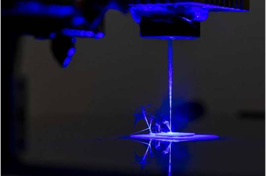
No assembly required: Innovative 3D printing method streamlines multi-materials manufacturing
University of Missouri researchers have developed a way to create complex devices with multiple materials—including plastics, metals and semiconductors—all with a single machine.
The research, which was recently published in Nature Communications, outlines a novel 3D printing and laser process to manufacture multi-material, multi-layered sensors, circuit boards and even textiles with electronic components.
It's called the Freeform Multi-material Assembly Process, and it promises to revolutionize the fabrication of new products.
By printing sensors embedded within a structure, the machine can make things that can sense environmental conditions, including temperature and pressure. For other researchers, that could mean having a natural-looking object such as a rock or seashell that could measure the movement of ocean water. For the public, applications could include wearable devices that monitor blood pressure and other vital signs.
Read more.
17 notes
·
View notes
Text
At Fine Trak System, we specialize in producing high-quality printed circuit boards (PCBs) that meet the diverse needs of various industries. From automotive to consumer electronics, we provide reliable and efficient PCB Fabrication in India that drives innovation and performance. We have a dedicated approach towards constant development. Hence, we invest regularly to meet the ever-increasing technological demands of our customers.
#PCB Fabrication in India#PCB Manufacturing Companies#PCB Manufacturing Services#Printed Circuit Board Manufacturer
1 note
·
View note
Text
ℙ𝕙𝕠𝕓𝕠𝕤 𝔹𝕒𝕟𝕟𝕖𝕣 - ℙ𝕖𝕣𝕤𝕠𝕟𝕒𝕝 𝕊𝕥𝕠𝕣𝕪
(SR) Lab Coats (Part 2): "It’d Make This Exchange a Lot Less Fun."

(Ignihyde Dorm: Lounge)
(Phobos appears to be working on something intently. A gentle hissing noise and smoke is wafting up from before him as he’s leaning over one of the tables in the lounge)
Phobos: Hm…
Ignihyde Mob A: Well? How’s she lookin’?
Phobos: …Pretty sure that’s about it. Just needs to get cleaned up a bit and it’ll be good to go.
(Phobos holds up the finished piece: a freshly printed and soldered circuit board.)
Phobos: Here it is. Should fit right in place to where the old one was installed in the server bay.
Ignihyde Mob A: That’s so cool…! I didn’t know you could just make those so easily!
Phobos: It’s not that hard. Just takes some time to learn how to do, like any other skill.
Phobos: All that’s left to do is let it cool and plug it back in. Let Idia know I’m gonna have that server back in working order soon enough.
Ignihyde Mob A: Yeah, for sure!
(The mob student takes off down the hall)
Ortho: That’s impressive work, Phobos Banner! You almost can’t tell the difference between the old circuit board and the new one, outside of the damage to the previous component of course.
Phobos: It better be impressive. I’ve been doing this for long enough that I’d hope my skills would translate to a print this simple at the very least.
Ortho: I’m a little surprised that you were able to make this circuit board without any assistance or machinery outside of an iron and a soldering gun.
Ortho: With my “Precision Gear” equipped I’m capable of performing many intricate and minute tasks that would be difficult or otherwise impossible for a human hand to perform.
Ortho: It has many tools and accessories that make it especially well-equipped for handling various medical procedures, but it can also easily be used for mechanical inspection and repair as well.
Ortho: My brother requested me to assist you with this task for this reason, but… aside from fetching you a few requested items, you hardly needed my help at all.
Phobos: Like I said, I’ve got experience with this sort of thing. I’ve been doing this for years now since I started learning how to build my own electronics from scratch.
Phobos: It helps to not have “human eyes”, too. My vision is better than most peoples’ in this dorm, easily.
Ortho: This is true! Your hands are quite steady too. You’re practically made for this kind of work!
Phobos: Heh… Appreciate the compliment.
Phobos: Anyway, I’m gonna start cleaning up my materials. Since you have the small hands for it, why don’t you take this circuit board and reinstall it for me back in the server for me.
(The sound of footsteps clack against the floor as someone approaches Phobos from afar.)
Rook: Bonjour!
Rook: I apologize for the delay, Roi du Poison required my steadfast presence and I could never say no to his demand.
Ortho: Oh! Good afternoon, Rook Hunt!
Rook: Monsieur Doll, a pleasure as always, as well~
Phobos: You actually showed up, huh. You really must have a death wish.
Rook: If it is by your hand it would be a death worth having experienced. I must admit, I’ve become slightly addicted to your penmanship.
Phobos: Ugh… Don’t make this weird. Here.
(Phobos hands a folded piece of paper to Rook)
Phobos: You remember our rules, right?
Rook: Oui.
Phobos: Good. Go ahead and read it whenever you want, then.
Ortho: Eh? A piece of paper?
Rook: Oui, but it is not just a simple piece of paper.
Rook: Written upon its surface is a delightful dance of poetry and prose, with words so tantalizingly powerful they rewire the very fabric of your being.
Rook: Never before have such simple words ever shaken me to my very core, hijacking my very essence and liberating my being from the very shackles of life to bring me momentarily to the edge of nirvana.
Rook: It’s truly an artistry! A rush of adrenaline, of life, like none I have ever experienced before!
Ortho: Really?! Phobos Banner, I had no idea you were such a poet!
Phobos: …It’s not exactly like that.
Ortho: Aw, but Rook Hunt seems to really admire your talent! I’d love to read some of your work, too!
Phobos: You- …Actually. I’ll think about it. It’d be interesting to see what a non-human reaction would be to it.
Phobos: Speaking of- you before said your currently equipped body is best suited for medical assistance. Do me a favor and stick around for a minute.
Ortho: Oh? Is something the matter? Are you feeling ill?
Rook: Ugh-!
(Rook collapses to the floor with a thud)
Ortho: Uwa?!
Phobos: No, but he probably is.
Ortho: Rook Hunt! What happened?!
Ortho: Commencing emergency bio-scans.
Ortho: Oxygen levels decreasing rapidly. Blood pressure levels dropping to dangerously low levels. Cause of emergency appears to be caused by sudden seizure of lung muscles.
Ortho: No viral presence detected. No venomous presence detected.
Ortho: Commencing emergency resuscitation.
Phobos: That won’t be necessary, Ortho. He’ll be fine.
Ortho: Wha-?! He’s going into shock, Phobos Banner! He’s very much not-!
Rook: (Gasps, then coughs roughly) It is... okay, Monsieur Doll... I am okay.
Ortho: Ah!! Rook Hunt! You’re… okay?
Ortho: Scanning… Blood oxygen levels normalizing. Blood pressure levels normalizing. Lung function normalizing.
Ortho: How is this possible…? I’ve never heard of the human body recovering from shock this quickly before.
Ortho: This note…
(Ortho picks up the note Phobos previously gave to Ortho and begins reading from it)
Ortho: “The body and mind intertwine; two halves are now one whole.
The mind becomes acutely aware of the body’s breath. The mind becomes aware that it must think in order for the body to breathe.”
Ortho: “The mind detests its exhaustion. Detests the command to further breath. Detests that it must process an unconscious action in order to sustain the body’s life. Lecherous and co-dependent, a leech that takes and never returns.”
Ortho: “The mind sets flame to its bridge to sever this connection of perceived toxicity. The mind seizes the body’s muscles, focuses on the chest, to stop the churning of oxygen through blood and flesh.”
Ortho: “Ribbons of capillaries tie together into knots, unable to be separated. Serpents intertwine in a delirious dance of death.”
Ortho: “In its fit of perceived righteousness the mind realizes still that the body and mind are one, and should one fall, the other shall follow.”
Ortho: “The bridge is only just alight, flames lick shallow against the boards that hold its weight against the pull of gravity. The mind stomps the flames into the dirt. The bridge is left unburnt.”
Ortho: “Ribbons untangle, deadly lovers separate from their dance. Air and blood flow free through muscle and bone.”
Ortho: “The mind and body become two halves once again. The mind is no longer aware of the body’s presence. Perceived co-dependence fades into hazy memories.”
Ortho: “Memories drift listlessly, ash in the wind trickling from the boards of a once-charred bridge.”
Ortho: This is… ah!
Rook: Ohh, Phobos… you’re a truly dastardly devil. Your words hold such power, such conviction. My body cannot help but follow each delicate letter’s command so tentatively.
Ortho: You-! Phobos Banner! You used magic against Rook Hunt through the words written on this note!
Ortho: You could have killed him! This is no better than if you had poisoned his drink and watched him collapse in front of you!
Phobos: Relax, Ortho. I’m not going to kill him. It’d make this exchange a lot less fun if I did.
Phobos: My unique magic “Terror Black” doesn’t take effect unless the entirety of the contained message is read in full. If he at least glosses over the fail-safe I included at the end he’ll be fine.
Phobos: Granted, I haven’t tested on what happens when I rip part of the message out of the original text… Hey Rook, I think I have an idea for a new abstract work I think will really take your breath away.
Rook: Tease me not, I can only become so enraptured in you before it becomes truly detrimental to my health.
Ortho: Rook Hunt, for the sake of your health I must recommend you not to continue in this reckless behavior.
Rook: Non, non… Monsieur Doll, despite your lively attitude you’ve yet to understand that which a human heart truly craves.
Ortho: Eh…?
Rook: The human heart craves beauty and artistry that truly envelops its entire being. True art and beauty can still the senses, numb pain, and steal away the body’s consciousness in a trance.
Rook: I’ve never before in my life experienced such art that was able to perform this duty so literally… I feel fortunate that I was able to find someone so beautifully talented!
Rook: Besides… it would betray my hunter’s blood to back away from a deadly challenge such as this. I must see this path through to the end, otherwise I’d never find the satisfaction I so dearly crave.
Ortho: I suppose so, but still… this seems to be too illogically dangerous for me to recommend at all in good faith.
Phobos: I’m not forcing him to take part in it; he can stop whenever he wants.
Phobos: But… if you’re still interested in reading some of my “poetry”, Ortho, I can write you something special, just for your eyes only.
Phobos: I’m a little more than interested to see how a machine might react to something I usually only let human eyes see.
Ortho: I’ll have to decline. Now that I know your intentions, I can’t find any merit in taking part in such an experiment.
Phobos: Eh. Offer’s on the table if you change your mind. I'm not gonna hurt you. Just... poke around a little on the insides. That's what this is all about.
Phobos: I know my way around machines way more than I know my way around human skin. If there’s anything you could trust me with, it’s your safety.
Phobos: You saw my handiwork earlier, at any rate. If there’s a couple things I’m skilled in tinkering with, it’s chemicals and circuitry.
/ End
#ツイステッドワンダーランド#Twisted Wonderland#TWST#twst oc#oc#original character#soul writes#personal story#Phobos Banner#フォボス • バナー
10 notes
·
View notes
Text
Printed Circuit Board Basics
Most of us are using Printed Circuit Board in our daily life. Printed Circuit Boards are used in almost all the Electronic products, from consumer gadgets such as PCs, tablets, smartphones, and gaming consoles to industrial and even high tech products in strategic and medical electronics domains.
Here, we have some statistics for you that shows how many electronic devices connect worldwide from 2015 to 2025. This statistic shows an increase in the use of a number of PCB in people daily life. Hence, CircuitWala took this opportunity to provide a basic knowledge about PCB via this article.
There are so many books available online which teach about Printed Circuit Board design and hardware part. There are few links available online which shows only a few basic fundamentals of PCB and few are there for Basics of Printed Circuit Board (PCB) Design. Few which gives good know knowledge on Printed Circuit Board terminology. But in the end for the hobbyist, there is no such material available which make their work easy.
Now days there few online designing websites available which allow hobbyist and students to create their design and Printed Circuit Board fabrication part. These websites provide limited features and charge high for the full edition. We, @CircuitWala are in try to provide one platform which provides plenty of Printed Circuit Board knowledge digitally to make your work simple and easy.
Alternatives of PCB include wire wrap and point-to-point construction. Creating a layout of PCB is a little bit time-consuming method as compared to its alternative solution but manufacturing of PCB is cheaper and faster then other wiring methods as electronic components are mounted and wired with one single part.
Let’s start with some basics of Printed Circuit Board with this article. Here in this article we will discuss about history of PCB to understand the emerge of PCB, Types of PCB to make your complex PCB a very simple using different types, Usage of PCB to provide you an idea to create more Printed Circuit Board projects, Advantages and Disadvantages, Possible Future to know about new technological change in Printed Circuit Board manufacturing and also about how to destroy and manage your PCB’s e-waste? We know you are eager to know all the stuff in details but before that let’s make a simple definition of Printed Circuit Board.
What is Printed Circuit Board?Printed Circuit Board is an electronic device made of conductive material(FR-4) like copper which connects components mounted on it to to get desired output by providing an input on another end.
When the board has not mounted with any of the components is called as Printed Circuit Board or Printed Wired Board. Mounting of an electronic component on Printed Circuit Board is called as PCB assembly.
History of Printed Circuit BoardThe invention of Printed Circuit Board was by Austrian engineer Paul Eisler as part of a radio set while working in England around 1936.
In early days before Printed Circuit Board became common in use, Point-to-Point construction was used. This meant some bulky and unreliable design that required plenty of sockets and regular replacement of it. Most of this issue directly address when PCB went into regular production.
Originally, every electronic component had wire leads, and the PCB had holes drilled for each wire of each component. The components’ leads were then passed through the holes and soldered to the PCB trace. This method of assembly is called Through-Hole construction. There is one other method to mount component is called as Surface Mount.
Type of Printed Circuit BoardPCBs are produced from the different types of material and on the basis of that material PCBs are divided mainly into two parts: Rigid PCB and Flexible PCB. Nowadays, a combination of Rigid and flexible PCB is also possible and that is called as Flexi-Rigid PCBs.
Most of the PCBs are built in layers. The inner layer is the base material called as a substrate. Rigid PCBs are mainly made of material like epoxy materials and Flexible PCBs are made of plastic material that can withstand high temperatures.
Rigid PCBs are generally, hard materials that hold the component in a better way. The motherboard in the tower of a computer is the best example of Rigid PCBs. Flexible PCBs fundamental material allows PCB to fit into forms that Rigid PCBs can not. Flexible PCBs can turn round without harmful the circuit on PCB.
All Rigid and Flexible PCBs can come in three formats by layers: Single Layer, Double Layer, and Multi-Layer.
1. Single Layer PCBSingle Layer PCBs have been around since the late 1950s and still dominate the world market in sheer piece volume. Single Sided PCBs contain only one layer of conductive material and are best suited for low-density designs. Single-sided PCBs are easy to design and quick to manufacture. They serve as the most lucrative platform in the industry.
2. Double Layer PCBDouble Layered printed circuit board technology is conceivably the most popular type of PCB in the industry. Double Sided PCB (also known as Double-Sided Plated Thru or DSPT) circuits are the gateway to advanced technology applications. They allow for a closer (and perhaps more) routing traces by alternating between top and bottom layers using vias.
3. Multi Layer PCB
Multilayer PCB is a circuit board that has more than two layers. Unlike a Double-Sided PCB which only has two conductive layers of material, all multilayer PCBs must have at least three layers of conductive material which are buried in the center of the material.
Usage of Printed Circuit BoardBy reading this article till this point, we hope that you are now able to get about printed circuit boards. Now, we will make you understand about different applications of printed Circuit Board.
In this digital world, Printed Circuit Board is in almost all our daily life electronic devices and in our industrial electronics as well. Below are the industries where PCBs are used:
Possible FutureNowadays, most of the circuits are replaced to produce Printed Circuit Board from the old methods. Revolution in technology made many of the processes automated and hence it is easy to manufacture PCB. But still, these processes are a bit expensive to hire, involve toxic waste and use high temperatures and acids. With technological advances we have seen in the past years, it is not hard to imagine PCB will soon be revolutionized. Not only that but research institutes predict a more ‘green’ future for PCBs; PCBs being made of paper.
Electronic Waste (e-waste)Electronic Waste or e-waste is described as discarded electrical or electronic devices. Informal processing of e-waste in developing countries can lead to adverse human health effects and environmental pollution.
Electronic scrap components contain a hazardous substance such as lead, cadmium, beryllium, or brominated flame retardants. Recycling and disposal of e-waste may involve significant risk to health of workers and communities in developed countries and great care must be taken to avoid unsafe exposure in recycling operations
Nowadays, developing countries are encouraging electronic users to take care while recycling the e-waste or submit them to the organization who are involved in such activities.
SummaryIn this blog, we have learned the basics of Printed Circuit Board. CircuitWala is planning to write as many blogs to provide more and more knowledge of Printed Circuit Board. Either it is basics or manufacturing or usages or advantages and disadvantages of PCBs. We will also try to make our users/customers up to date for the new technology innovations, including past histories and revolution of the PCB industries.
In the next blog, we will look at more briefly about the different types of Printed Circuit Board. We also understand the process to make it and different usage and application for the same.
#electronic circuit design company#pcb circuit manufacturer in ahmedabad#pcb design & manufacturing services#printed circuit board companies#printed circuit board order online#PCB manufacturer#Printed Circuited Board#double layer PCB#PCB Quality Control
2 notes
·
View notes
Text
Elevating Industry Standards: PVDF Materials by Petron Thermo Plast
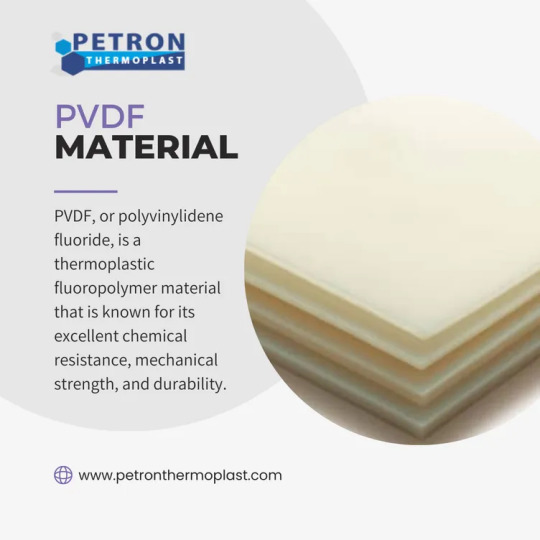
In the dynamic landscape of industrial materials, Polyvinylidene Fluoride (PVDF) emerges as a standout choice, renowned for its exceptional properties and diverse applications. Petron Thermo Plast, a leading manufacturer in the field, specializes in delivering top-tier PVDF Materials crafted to surpass industry expectations. This blog meticulously explores the features, benefits, and applications of PVDF materials by Petron Thermo Plast, showcasing why they are the preferred solution for professionals worldwide.
Unveiling PVDF Materials
PVDF materials represent a pinnacle of innovation, characterized by their remarkable chemical resistance, thermal stability, and mechanical strength. Petron Thermo Plast’s PVDF materials are engineered with precision to offer unparalleled performance across a multitude of industrial settings.
Key Attributes of PVDF Materials
1. Chemical Resistance:
PVDF materials exhibit exceptional resistance to a wide spectrum of chemicals, including acids, bases, and solvents, making them ideal for corrosive environments.
2. Thermal Stability:
With a high melting point and remarkable heat resistance, PVDF materials maintain their integrity even under extreme temperatures, ensuring reliability in demanding conditions.
3. Mechanical Strength:
PVDF materials boast high tensile strength and durability, enabling them to withstand mechanical stress and pressure, thus guaranteeing longevity in challenging applications.
4. Low Permeability:
The low permeability of PVDF materials to gases and liquids prevents leakage, making them suitable for applications requiring excellent barrier properties.
5. Weatherability:
PVDF materials exhibit exceptional weather resistance, making them suitable for outdoor applications where exposure to UV radiation and harsh weather conditions is common.
6. Non-Toxicity:
PVDF materials are non-toxic and safe for use in applications involving potable water and food processing, adhering to stringent health and safety standards.
Applications of PVDF Materials
PVDF materials by Petron Thermo Plast find extensive applications across diverse industries:
Chemical Processing: Used for fabricating pipes, fittings, and linings in chemical plants due to their resistance to corrosive chemicals.
Construction: Employed in architectural cladding, roofing, and facades for their durability and weather resistance.
Electronics: Utilized in printed circuit boards and semiconductor manufacturing for their electrical insulation properties.
Transportation: Applied in aerospace and automotive industries for interior and exterior components due to their lightweight and high strength-to-weight ratio.
Medical: Used in medical equipment and devices requiring sterilizability and chemical resistance.
Advantages of Choosing Petron Thermo Plast
Advanced Manufacturing Techniques:
Petron Thermo Plast employs cutting-edge manufacturing processes and rigorous quality control measures to ensure PVDF materials meet the highest standards.
Customization Options:
The company offers PVDF materials in various formulations, sizes, and colors to meet specific customer requirements.
Expert Technical Support:
Comprehensive technical support and guidance are provided to assist customers in selecting the right PVDF materials and ensuring proper integration into their projects.
Sustainability Commitment:
Petron Thermo Plast is committed to sustainable manufacturing practices, ensuring their PVDF materials are environmentally friendly and compliant with global standards.
Why Choose PVDF Materials from Petron Thermo Plast?
Investing in PVDF materials from Petron Thermo Plast guarantees superior quality, reliability, and performance. Here are some compelling reasons to choose Petron Thermo Plast:
Unmatched Quality: PVDF materials from Petron Thermo Plast adhere to the highest quality standards, ensuring consistency and reliability.
Tailored Solutions: With a wide range of formulations and customization options available, you can find the perfect PVDF material for your specific application.
Technical Expertise: Petron Thermo Plast provides expert technical support to guide you through every stage, from material selection to project completion.
Sustainability: By choosing PVDF materials from Petron Thermo Plast, you are supporting environmentally friendly manufacturing practices and contributing to a greener future.
Conclusion
PVDF materials by Petron Thermo Plast redefine excellence in the industrial sector. Their unparalleled properties, reliability, and versatility make them indispensable across various industries. Choose Petron Thermo Plast for PVDF materials that exceed your expectations and elevate your projects to new heights of success.
#pvdf material#engineering plastics#pvc ball valve#pvc butterfly valve#pvdf pipe#explore#union ball valve#hdpe pipe fittings
2 notes
·
View notes
Last Seen Blogs

julian--the--janitor
The Great Recitating Platypus Is Real

binnikki
⠀⠀ ⠀⠀⠀⠀ ⠀⠀⠀⠀ ⠀⠀⠀⠀

rightchoiceconsultingblog
Untitled

lionliving
LionLiving

peytona
Sin título