
High Quality PCB Co., Ltd. - A leading IC substrate and PCB assembly specialist since 2006 in China. We specialize in: • IC substrates (up to 18 layers, 0.25mm BGA pitch) • Substrate-like PCB assembly • Modular PCB assembly Our strength lies in cutting-edge technology, reliable quality, and full-cycle support from design to mass production. Serving global clients in communications, automotive, aerospace, medical, and military sectors, we export 76.7% of products to Europe, America, and Asia-Pacific markets. Key advantages: ✓ Advanced manufacturing capabilities ✓ Prototype-to-volume production ✓ Competitive solutions ✓ Technical excellence
Don't wanna be here? Send us removal request.
Statistics
We looked inside some of the posts by icsubstrate and here's what we found interesting.
Average Info
Notes Per Post
5
Likes Per Post
5
Reblog Per Post
0
Reply Per Post
0
Time Between Posts
8 days
Number of Posts By Type
Text
10
Last Seen Tumblr Blogs


Fun Fact
Celebrities use Tumblr as well.
Text

How to Choose IC Substrate Manufacturers?
The integrated circuit (IC) substrate is a cornerstone of modern semiconductor packaging, enabling the seamless connection between chips and printed circuit boards (PCBs). As the demand for advanced technologies like 5G, AI, and IoT continues to rise, selecting the right IC substrate manufacturer has become a critical decision for businesses aiming to stay competitive. This article delves into the essential factors to consider when choosing an IC substrate manufacturer, with a focus on product features, technical expertise, and industry trends.
The Importance of IC Substrates in Modern Electronics
IC substrates are not just passive components; they are the backbone of semiconductor devices, providing electrical connectivity, mechanical support, and thermal management. They are used in advanced packaging technologies such as flip-chip, ball grid array (BGA), and fan-out wafer-level packaging (FOWLP). As devices become smaller, faster, and more complex, the requirements for IC substrates—such as finer line widths, higher density, and improved thermal performance—have become increasingly stringent.
The global IC substrate market is projected to grow at a compound annual growth rate (CAGR) of 6.5% from 2023 to 2028, driven by the proliferation of high-performance computing, automotive electronics, and consumer devices. This growth underscores the need for manufacturers who can deliver cutting-edge solutions tailored to diverse applications.
Key Factors to Consider When Choosing an IC Substrate Manufacturer
Technical Expertise and Innovation
The technical capabilities of an IC substrate manufacturer are paramount. Look for manufacturers with expertise in advanced processes such as fine-line patterning, multilayer lamination, and microvia formation. These capabilities are essential for producing substrates that meet the demands of high-frequency, high-power, and miniaturized devices.
For example, leading manufacturers like Ibiden and AT&S are known for their ability to produce substrates with line widths as small as 5 micrometers, enabling the development of next-generation chips for AI and 5G applications. Partnering with such manufacturers ensures that your products remain at the forefront of technological innovation.
Product Quality and Reliability
Quality is non-negotiable in the semiconductor industry. A reliable IC substrate manufacturer will have robust quality control systems in place, including ISO certifications, statistical process control (SPC), and advanced testing protocols. These measures ensure consistent performance and minimize the risk of defects or failures in your end products.
Moreover, manufacturers with a proven track record of high yields and low defect rates are more likely to deliver substrates that meet your specifications. For instance, Shinko Electric Industries has earned a reputation for its high-quality substrates used in automotive electronics, where reliability is critical.
Customization and Design Support
Every application has unique requirements, and off-the-shelf solutions may not always suffice. Leading IC substrate manufacturers offer customization services to tailor substrates to your specific needs. This includes material selection, layer count optimization, and layout design to enhance performance and manufacturability.
For example, Unimicron provides bespoke substrate solutions for applications ranging from smartphones to medical devices. Their design support teams work closely with clients to optimize substrate layouts, ensuring that the final product meets both technical and cost objectives.
Production Capacity and Scalability
As the demand for semiconductors continues to grow, production capacity has become a key consideration. Evaluate whether the IC substrate manufacturer can handle your volume requirements, both now and in the future. Manufacturers with multiple production facilities and flexible capacity are better equipped to meet your needs as your business scales.
The global semiconductor shortage in recent years highlighted the importance of supply chain resilience. Choosing a manufacturer with diversified sourcing strategies and contingency plans can help mitigate risks and ensure uninterrupted supply.
Cost-Effectiveness
While quality and performance are critical, cost is always a factor. Compare the pricing structures of different IC substrate manufacturers, taking into account material costs, production efficiency, and economies of scale. However, avoid compromising on quality to save costs, as this can lead to higher expenses in the long run due to product failures or recalls.
Geographic Location and Supply Chain Stability
The location of the IC substrate manufacturer can impact lead times, shipping costs, and access to advanced technologies. Manufacturers located in regions with robust semiconductor ecosystems—such as Taiwan, South Korea, and Japan—often have a competitive edge in terms of innovation and supply chain stability.
Additionally, consider the manufacturer’s ability to mitigate supply chain risks. The COVID-19 pandemic and geopolitical tensions have underscored the importance of supply chain resilience. Look for manufacturers with diversified sourcing strategies and contingency plans to ensure uninterrupted supply.
Reputation and Customer Reviews
Finally, research the reputation of the IC substrate manufacturer. Look for customer reviews, testimonials, and case studies to gauge their reliability and performance. A manufacturer with a strong reputation is more likely to deliver on their promises and provide excellent customer service.
Leading IC Substrate Manufacturers in the Market
To provide a benchmark, here are some of the top IC substrate manufacturers globally:
Ibiden: Known for its advanced flip-chip substrates and focus on high-performance computing applications.
High Quality PCB: Specializes in IC substrates for memory modules and automotive electronics.
AT&S: A leader in high-end IC substrates for 5G and IoT applications.
Unimicron: Offers a wide range of substrates, including those for advanced packaging technologies.
Semco (Samsung Electro-Mechanics): Focuses on substrates for smartphones, tablets, and wearable devices.
These manufacturers have established themselves as industry leaders through their technical capabilities, quality standards, and innovation.
FAQs
What is the role of an IC substrate in semiconductor packaging?
IC substrates provide electrical connections between the chip and the PCB, along with mechanical support, thermal dissipation, and signal integrity. They are essential for ensuring the performance and reliability of semiconductor devices.
How do I evaluate the quality of an IC substrate manufacturer?
Look for manufacturers with ISO certifications, advanced testing capabilities, and a track record of low defect rates. Customer reviews and case studies can also provide insights into their quality standards.
Why is geographic location important when choosing an IC substrate manufacturer?
The location can impact lead times, shipping costs, and access to advanced technologies. Manufacturers in regions with strong semiconductor ecosystems often have an advantage in terms of innovation and supply chain stability.
Can IC substrate manufacturers provide customized solutions?
Yes, many leading manufacturers offer customization services to tailor substrates to specific applications. This may include design support, material selection, and layout optimization.
Who are the top IC substrate manufacturers?
Some of the top manufacturers include Ibiden, Shinko Electric Industries, AT&S, Unimicron, and Samsung Electro-Mechanics.
Conclusion
Choosing the right IC substrate manufacturer is a critical decision that can significantly impact the performance, reliability, and cost of your products. By evaluating factors such as technical capabilities, quality standards, production capacity, and reputation, you can identify a manufacturer that aligns with your needs. As the demand for advanced IC substrates continues to grow, partnering with a reliable and innovative manufacturer will ensure your success in the competitive semiconductor market.
0 notes
Text

IC Substrate Manufacturing Technology Guide (2025)
IC bundled substrate fabrication is the foundation of the electronics industry, that has lead to the creation of the most sophisticated semiconductor devices that is at the core of today's technology. As we enter the year 2025, rank of high-performance embedded, miniaturized and low-power consumption devices is increasing and is pushing novelty in IC substrate fabrication. Comprehensive and in-depth discussion of manufacturing strategies, techniques, and technologies of ultra-violet LEDs for electricity saviorThis edited volume on ultra-violet (UV) light emitting diodes provide an overview of UV light, devices, and applications.
What is IC Substrate Manufacturing?
IC substrate production is responsible for the production of the base layer (it is the bridge between semiconductor chips and PCBs). These substrates act as a connective, electrical, thermal and mechanical link. IC substrate production is a critical link in application from consumer electronics to high-performance computing and communication.
The IC Substrate Manufacturing Process
Material Selection
The process begins with the careful selection of materials, which directly impact the substrate's performance. Common materials include:
FR-4 (Fiberglass Reinforced Epoxy): Widely used for cost-effective and standard applications.
BT Resin (Bismaleimide-Triazine): Known for its high thermal stability and low dielectric loss, making it ideal for high-frequency applications.
Ceramic Substrates: Preferred for their excellent thermal conductivity and reliability in high-power applications.
Advanced Polymers: Materials like liquid crystal polymers (LCPs) are gaining traction due to their superior electrical and thermal properties.
Substrate Design
Substrate design is a critical step that involves creating a detailed layout of conductive traces, vias, and pads. Advanced software tools are used to optimize the design for electrical performance, signal integrity, and manufacturability.
Lamination
Lamination bonds multiple layers of material to form the substrate. This process includes:
Prepreg Preparation: Layers are pre-impregnated with resin to ensure adhesion.
Heat and Pressure Application: Controlled heat and pressure are applied to achieve uniform thickness and structural integrity.
Drilling
Drilling creates vias, which are vertical connections between different layers. Techniques include:
Mechanical Drilling: Suitable for larger vias.
Laser Drilling: Enables precise microvias, essential for high-density interconnects.
Plating and Etching
Plating deposits a conductive layer, typically copper, onto the substrate. Etching removes excess copper to define the circuit patterns. This step ensures electrical connectivity and minimizes signal interference.
Solder Mask Application
A solder mask is applied to protect the substrate's surface and prevent soldering errors during assembly. This mask is typically made of epoxy-based materials and applied using screen printing or photolithography.
Testing and Inspection
Quality control is paramount in IC substrate manufacturing. Testing methods include:
Electrical Testing: Verifies conductivity and insulation.
Visual Inspection: Identifies physical defects such as cracks or delamination.
X-Ray Inspection: Detects internal defects and ensures layer alignment.
Advancements in IC Substrate Manufacturing Technology
High-Density Interconnect (HDI) Technology
HDI technology enables the production of substrates with finer traces and microvias, supporting higher component density and improved signal integrity. This is particularly important for applications like 5G and IoT devices.
Embedded Component Technology
This innovation integrates passive components directly into the substrate, reducing size and enhancing performance. It is a game-changer for miniaturized devices.
Advanced Materials
The development of new materials, such as liquid crystal polymers (LCPs) and organic substrates, offers improved thermal and electrical properties, paving the way for next-generation devices.
Challenges in IC Substrate Manufacturing
Cost Management
The production of high-performance substrates involves expensive materials and processes, posing challenges for cost optimization. Manufacturers are exploring ways to balance performance and affordability.
Miniaturization
As devices become smaller, achieving precise designs and maintaining reliability becomes increasingly difficult. Advanced manufacturing techniques and materials are essential to address this challenge.
Environmental Concerns
The use of chemicals and energy-intensive processes raises environmental issues. The industry is shifting toward sustainable practices, such as recycling and reducing waste.
Frequently Asked Questions (FAQ)
What is the role of IC substrates in electronic devices?
IC substrates provide mechanical support and electrical connections between semiconductor chips and PCBs, enabling the functionality of electronic devices.
What materials are commonly used in IC substrate manufacturing?
Common materials include FR-4, BT resin, ceramic substrates, and advanced polymers like LCPs.
How does HDI technology improve IC substrates?
HDI technology enhances substrate performance by enabling finer traces, microvias, and higher component density.
What are the environmental challenges in IC substrate manufacturing?
The process involves the use of chemicals and energy-intensive methods, leading to concerns about waste management and carbon emissions.
Conclusion
The production process of IC substrates has been a developing and expanding industry in which the field serves as the electronic industry cornerstone. Looking toward 2025, there will be ever-greater material, technology, and process-based developments for Filipet to exploit. By focusing on cost control, miniaturization, and environmental friendliness, manufacturers can satisfy the increasing demand for high-performance IC substrates and contribute to the future of electronics.
1 note
·
View note
Text
How to Manufacture mSAP Substrate?
In the relentless pursuit of smaller, faster, and more powerful electronic devices, the underlying components must evolve at a blistering pace. One of the most significant advancements in this arena is the mSAP substrate. Standing for "modified Semi-Additive Process," this technology has become a cornerstone for creating the high-density interconnect (HDI) printed circuit boards (PCBs) and semiconductor packages that power everything from flagship smartphones to advanced automotive systems. Understanding its manufacturing process reveals a sophisticated blend of chemistry, physics, and precision engineering.
This article provides a comprehensive overview of how an mSAP substrate is made, detailing the technical workflow, the innovations driving the industry forward, and the inherent challenges that manufacturers must overcome to produce these intricate components.
What Is an mSAP Substrate?
Before diving into the manufacturing process, it's essential to understand what an mSAP substrate is and why it's so crucial. Traditional circuit board manufacturing often relies on a "subtractive" method, where a full layer of copper is laminated onto a board, and the unwanted copper is chemically etched away to leave the desired circuit traces. This method has limitations, particularly when it comes to creating very fine lines and spaces.
The modified Semi-Additive Process, in contrast, builds the circuit traces up. It starts with a very thin seed layer of copper and then selectively adds more copper only where the circuit is needed. This additive approach allows for the creation of exceptionally fine circuit lines and spaces, often below 30 microns, a feat difficult or impossible to achieve with purely subtractive methods. Consequently, the mSAP substrate enables greater circuit density, leading to smaller form factors, improved electrical performance, and higher functionality in the final electronic product. The development of the mSAP substrate has been a key enabler for the miniaturization trend seen across the tech industry.
The Manufacturing Workflow of an mSAP Substrate
The production of an mSAP substrate is a multi-stage process that demands a cleanroom environment and stringent process controls. Each step is critical to achieving the high yields and reliability required for modern electronics.
Material Selection and Preparation
The journey begins with the base materials. The core of the substrate is typically a dielectric material, such as an advanced epoxy resin blend or polyimide, which provides electrical insulation and structural integrity. A very thin copper foil, often just 1 to 3 microns thick, is laminated onto this core. This initial thin copper is a key differentiator for the mSAP process and is crucial for the subsequent steps. The quality of these raw materials directly influences the final performance and reliability of the mSAP substrate.
The Core of the Process: Modified Semi-Additive Plating
This is where the magic happens and what gives the mSAP substrate its name. The process involves several intricate steps:
Surface Activation: The thin copper foil is thoroughly cleaned and treated to ensure it is ready for plating. This often involves a chemical process that creates a micro-roughened surface to promote adhesion.
Imaging and Patterning: A layer of light-sensitive material, known as a photoresist, is applied over the entire surface. Using photolithography, a UV light source projects the circuit pattern onto the resist. The areas exposed to light (or shielded from it, depending on the type of resist) are hardened. The unhardened resist is then washed away, leaving a stencil-like pattern that exposes the thin copper seed layer only where the final circuit traces should be.
Electrolytic Copper Plating: The substrate is submerged in an electrolytic plating bath. An electric current is applied, causing copper ions from the solution to deposit onto the exposed seed layer. The copper builds up vertically and horizontally, forming the thick, highly conductive circuit traces. The thickness of this plated copper is precisely controlled to meet the design's electrical requirements. This additive step is the heart of what makes an mSAP substrate so capable of producing fine lines.
Resist Stripping and Etching: Once the traces are plated to the desired thickness, the remaining hardened photoresist is chemically stripped away. This reveals the newly formed copper circuits sitting atop the original thin seed layer. A final, quick "flash" etching step is performed to remove the now-unwanted seed layer from the areas between the circuit traces. Because this etching step only removes a very thin layer of copper, it avoids the undercutting issues common in subtractive processes, thus preserving the fine-line definition of the mSAP substrate.
Building Complexity: Multi-Layer Lamination and Vias
Most modern devices require multi-layer boards. To create a multi-layer mSAP substrate, the core process is repeated. Layers of dielectric material are pressed and laminated on top of the completed circuit layer. To connect the different layers electrically, tiny holes called "microvias" are drilled using high-precision lasers. These vias are then plated with copper, creating vertical pathways for signals to travel between layers. This build-up process can be repeated multiple times to create a complex, high-density mSAP substrate with a dozen or more layers.
Finalizing the Board: Surface Finish and Solder Mask
After the layers are built and interconnected, a solder mask is applied. This is the typically green, blue, or black coating seen on circuit boards. It protects the copper traces from oxidation and prevents solder bridges from forming between adjacent pads during component assembly. Finally, a surface finish, such as Electroless Nickel Immersion Gold (ENIG), is applied to the exposed copper pads where components will be soldered. This ensures a reliable, solderable, and corrosion-resistant surface for the final assembly of the mSAP substrate.
Key Innovations Shaping the Future of mSAP Substrate Production
The technology behind the mSAP substrate is not static. Continuous innovation is pushing the boundaries of what is possible. This includes the development of new dielectric materials with better thermal properties and lower signal loss, as well as advancements in laser drilling technology that allow for even smaller and more precisely placed microvias. The industry is constantly striving to reduce line widths even further, with some manufacturers now capable of producing features below 10 microns on a commercial mSAP substrate.
Overcoming Hurdles in mSAP Substrate Manufacturing
Despite its advantages, producing a high-quality mSAP substrate is not without its challenges. The process is highly sensitive to contamination, requiring pristine cleanroom conditions. Achieving high yields is a constant battle, as even a microscopic defect can render a complex board useless. Furthermore, the capital investment for mSAP equipment is substantial, and managing the complex chemical processes requires significant expertise. Thermal management within the densely packed circuits of an mSAP substrate is another critical concern that designers and manufacturers must address.
Frequently Asked Questions (FAQs)
What is an mSAP substrate?
An mSAP substrate is a type of high-density interconnect (HDI) circuit board manufactured using the modified Semi-Additive Process. This process allows for the creation of extremely fine circuit lines by plating copper onto a thin seed layer, rather than etching it away from a thick one.
Why is the mSAP process better than traditional subtractive methods?
The mSAP process offers superior fine-line capability, enabling greater circuit density and miniaturization. It minimizes the undercutting effect seen in subtractive etching, resulting in traces with sharper, more defined profiles, which improves electrical performance, especially at high frequencies.
What are the main applications for an mSAP substrate?
The mSAP substrate is primarily used in high-performance, space-constrained electronics. This includes smartphone mainboards (SLPs or Substrate-Like PCBs), semiconductor packages (e.g., for GPUs and CPUs), wearable devices, and advanced modules for 5G and IoT applications.
What are the key challenges in mSAP substrate production?
The main challenges include maintaining extremely high levels of cleanliness to avoid defects, achieving high manufacturing yields on complex multi-layer boards, managing the high cost of equipment and materials, and engineering effective thermal dissipation for densely packed components.
Conclusion
The manufacturing of an mSAP substrate represents the pinnacle of modern circuit board technology. It is a testament to the incredible precision that can be achieved when advanced chemical processes are combined with sophisticated engineering. While the workflow is complex and demanding, the result is a component that enables the powerful, miniaturized devices that define our modern world. As technology continues to advance, the role of the mSAP substrate will only become more critical, serving as the intricate nervous system for the next generation of electronics.
0 notes
Text

How to Manufacture a Micro SD Card Substrate?
In the world of contemporary electronics, the humble micro SD card is a triumph of miniaturization and data density. Hmm, what could be missing is the little sexy device, which is embedded directly in the middle of this technology – but its core is micro SD card substrate! This layer of complexities is the base on which the controllers of the memory chips are constructed and it offers the structural strength and the electrical footprint required for the card to operate. The production of a micro SD card substrate is a highly complex venture that combines the finest aspect of material science, precision engineering and cutting-edge manufacturing processes. This article discusses the technical process chain, major innovations and associated challenges when manufacturing this essential component.
The Basis of substrate Micro SD memory card
Before learning about how the micro SD card is made, you might want to know what a substare for micro SD card is, and more importantly, the roles it plays. It is not just a lump of plastic; it is a sophisticated printed circuit board (PCB) designed to a high degree of precision. Its primary functions are threefold:
Mechanical Support: It provides a rigid, stable platform for the delicate silicon die (memory and controller chips).
Electrical Interconnection: It contains a dense network of conductive copper traces and microvias that route signals between the chips and the card's external contact pads.
Thermal Management: It helps dissipate the heat generated by the chips during operation, preventing performance degradation and ensuring longevity.
Given the tiny footprint of a micro SD card (15mm x 11mm), the design and production of the micro SD card substrate demand exceptional accuracy.
The Manufacturing Workflow: From Concept to Component

The creation of a micro SD card substrate is a multi-stage journey that begins with digital design and ends with a physically realized, rigorously tested component.
Material Selection and Core Preparation
The process begins with the careful selection of raw materials. The core of the substrate is typically a laminate composed of woven glass fiber cloth impregnated with epoxy resin, often FR-4 or a higher-performance equivalent with better thermal and electrical properties. Thin copper foils are bonded to both sides of this core material. The choice of materials is critical; according to industry data, dielectric constant (Dk) and dissipation factor (Df) are key parameters that influence signal integrity at high frequencies, making high-performance laminates essential for modern UHS (Ultra High Speed) cards.
Design and Circuit Imaging
Engineers use sophisticated CAD software to lay out the intricate circuitry. This digital blueprint defines the location of every trace, pad, and via. Once the design is finalized, it is transferred to the copper-clad core using photolithography. A layer of light-sensitive material called photoresist is applied to the copper. The circuit pattern is then exposed onto the resist using UV light, hardening the areas that will form the circuitry. The unhardened resist and the underlying copper are then chemically etched away, leaving behind the desired conductive pattern. This step is repeated for each layer of the micro SD card substrate.
The Build-Up Process and Lamination
Most modern micro SD cards require a multi-layered substrate to accommodate the complex wiring. The real artistry in manufacturing a micro SD card substrate lies in the build-up process. This involves stacking and laminating multiple layers of circuitry and insulation.
Layer Alignment: Inner layers are precisely aligned using registration holes.
Lamination: The stacked layers are fused together under immense pressure and high temperature in a lamination press. This process solidifies the resin and creates a single, robust board.
Drilling Microvias: To connect the different layers electrically, tiny holes called microvias are drilled. While traditional mechanical drilling is used for larger holes, laser drilling is the standard for the microscopic vias required in a high-density micro SD card substrate. Lasers can create vias with diameters of less than 75 microns, a feat impossible with mechanical drills.
Plating and Surface Finishing
After drilling, the vias are hollow and non-conductive. The entire panel, including the inside of the vias, is then plated with a thin layer of copper through an electroless plating process, followed by electrolytic plating to build up the required thickness. This creates the vertical electrical connections between the layers.
The final surface finish is then applied to the external pads. This is typically an Electroless Nickel Immersion Gold (ENIG) finish. The nickel layer provides a barrier, and the thin gold layer ensures excellent solderability and protects against oxidation. This finishing is vital for the reliability of the final micro SD card substrate.
Solder Mask and Silkscreen
A solder mask, a thin polymer coating (usually green, black, or blue), is applied over the entire surface of the micro SD card substrate, leaving only the contact pads exposed. This mask prevents solder bridges from forming between adjacent pads during chip assembly. Finally, a silkscreen layer with component designators or branding may be printed on the surface.
Rigorous Quality Assurance
Before being shipped for assembly, every micro SD card substrate undergoes a battery of tests. Automated Optical Inspection (AOI) uses cameras to scan for physical defects like short circuits, open circuits, or incorrect trace widths. Electrical testing, often using a "flying probe" or "bed-of-nails" tester, verifies every connection to ensure the substrate matches the design's electrical specifications perfectly.
Key Technological Innovations Shaping Production
The manufacturing of the micro SD card substrate is constantly evolving. High-Density Interconnect (HDI) technology is now standard, allowing for finer lines and spaces and the use of blind and buried vias to maximize routing density. Furthermore, the trend towards embedding passive components like resistors and capacitors directly within the substrate layers is gaining traction, further reducing the final card's size and improving electrical performance.
Overcoming Critical Manufacturing Hurdles
Producers face significant challenges. The relentless drive for miniaturization puts immense pressure on manufacturing tolerances. Thermal management is another critical hurdle; as card speeds increase, so does heat generation, requiring innovative thermal designs within the micro SD card substrate itself. Finally, maintaining extremely high yields while managing the cost of advanced materials and processes is a constant balancing act for every manufacturer of the micro SD card substrate.
Frequently Asked Questions (FAQs) About Micro SD Card Substrate Manufacturing
What are the primary materials in a micro SD card substrate?
The core is typically an epoxy-resin laminate (like FR-4), with conductive layers made of copper foil. The surface finish is often Electroless Nickel Immersion Gold (ENIG) for solderability and protection.
How are the microscopic holes (microvias) made?
Microvias are created using high-precision CO2 or UV laser drilling systems. This technology allows for the creation of extremely small and accurately placed holes needed to connect the dense layers of the micro SD card substrate.
Why is the solder mask layer important?
The solder mask protects the copper traces from oxidation and, most importantly, prevents solder from accidentally bridging between closely spaced contact pads during the chip mounting process, which would cause a short circuit.
What is the biggest challenge in manufacturing a micro SD card substrate?
The primary challenge is achieving extreme miniaturization while maintaining perfect electrical integrity and high production yields. Balancing the fine features, layer alignment, and material stability at such a small scale requires state-of-the-art equipment and process control.
How does HDI technology benefit the micro SD card substrate?
High-Density Interconnect (HDI) technology allows for finer lines and spaces, smaller vias, and higher layer counts. This enables designers to pack more functionality into the limited space of the micro SD card substrate, which is essential for high-capacity and high-speed cards.
Conclusion
It is an example of technology in micro SD card substrate production. It’s a trek of precision, from the choice of exotic materials to the ballet of lamination, laser drilling and chemical enhancements. Although the end-user only sees the final, small memory card, the micro SD substrate that lies underneath is a feat of engineering that allows it all to happen. The technology and methods behind making these crucial building blocks will surely become more sophisticated as data-storage demands grow ever larger.
0 notes
Text

How to Manufacture FMC Substrate: A Comprehensive Guide to Advanced Packaging Technology
The semiconductor industry has witnessed remarkable evolution in packaging technologies, with FMC substrate emerging as a cornerstone of modern electronic manufacturing. This specialized component serves as the foundation for flip-chip multi-chip modules, enabling unprecedented levels of integration and performance in today's sophisticated electronic devices. Understanding the intricate manufacturing process behind FMC substrate production reveals the complexity and precision required in contemporary semiconductor fabrication.
Understanding the Fundamentals of FMC Substrate Technology
FMC substrate represents a critical advancement in semiconductor packaging, designed specifically to accommodate flip-chip mounting configurations. These substrates provide the essential electrical pathways, mechanical support, and thermal management capabilities necessary for high-performance electronic assemblies. The manufacturing of FMC substrate requires sophisticated equipment, precise process control, and extensive quality assurance protocols to meet the demanding specifications of modern applications.
According to industry research from SEMI, the global substrate market for advanced packaging reached $15.2 billion in 2023, with FMC substrate applications accounting for approximately 28% of this market segment. This growth trajectory reflects the increasing demand for miniaturized, high-performance electronic devices across consumer electronics, automotive, and telecommunications sectors.
Core Materials and Design Considerations
The foundation of any successful FMC substrate begins with careful material selection and design optimization. Engineers typically utilize advanced organic materials such as ABF (Ajinomoto Build-up Film) or modified epoxy resins as the primary dielectric layers. These materials offer exceptional dimensional stability, low dielectric constant values, and excellent adhesion properties essential for reliable FMC substrate performance.
Copper foil selection plays an equally critical role, with manufacturers often choosing ultra-thin copper layers ranging from 3 to 12 micrometers in thickness. The choice depends on the specific electrical requirements and the intended application of the final FMC substrate assembly. Design engineers must carefully balance trace width, spacing, and layer count to optimize signal integrity while maintaining manufacturing feasibility.
Primary Manufacturing Process Flow
Substrate Preparation and Base Layer Formation
The manufacturing journey of FMC substrate begins with substrate preparation, where the base material undergoes thorough cleaning and surface treatment. This initial step ensures optimal adhesion between subsequent layers and eliminates contaminants that could compromise the final product's reliability. The base copper foil is typically treated with specialized chemical solutions to enhance surface roughness and promote strong bonding with dielectric materials.
Build-Up Layer Construction
The build-up process represents the heart of FMC substrate manufacturing, involving sequential deposition of dielectric and conductive layers. Each dielectric layer is applied using advanced lamination techniques under precisely controlled temperature and pressure conditions. Industry standards typically specify lamination temperatures between 180-220°C with pressures ranging from 2-4 MPa, depending on the specific material system employed.
Following dielectric layer application, the FMC substrate undergoes via formation through laser drilling or plasma etching processes. Modern laser drilling systems can achieve via diameters as small as 25 micrometers with aspect ratios exceeding 10:1, enabling high-density interconnect designs essential for advanced FMC substrate applications.
Metallization and Circuit Formation
Metallization processes follow via formation, typically involving electroless copper deposition followed by electrolytic copper plating. The electroless copper provides a conductive seed layer within the vias, while electrolytic plating builds up the required copper thickness for reliable electrical connections. Process parameters such as plating current density, bath temperature, and plating time are carefully controlled to ensure uniform copper distribution throughout the FMC substrate structure.
Circuit pattern formation utilizes advanced photolithography techniques, employing high-resolution photoresists and precision exposure systems. Line widths as narrow as 15 micrometers are routinely achieved in production FMC substrate manufacturing, with some advanced facilities capable of 10-micrometer features for specialized applications.
Advanced Manufacturing Technologies
High-Density Interconnect Implementation
Modern FMC substrate manufacturing increasingly relies on HDI (High-Density Interconnect) technology to achieve the miniaturization demands of contemporary electronic devices. HDI implementation involves multiple build-up layers with stacked microvias, enabling routing densities that would be impossible with conventional PCB technologies. Research from IPC indicates that HDI-based FMC substrate designs can achieve interconnect densities exceeding 2000 connections per square centimeter.
Embedded Component Integration
Advanced FMC substrate manufacturing may incorporate embedded passive components directly within the substrate layers. This integration technique, known as embedded component technology, allows resistors, capacitors, and inductors to be placed within the dielectric layers, reducing overall assembly height and improving electrical performance. The embedded components are typically screen-printed using specialized conductive and resistive inks, then cured at temperatures compatible with the surrounding dielectric materials.
Quality Control and Testing Protocols
Rigorous quality control measures are essential throughout FMC substrate manufacturing to ensure product reliability and performance. Automated optical inspection (AOI) systems examine each layer for defects such as opens, shorts, and dimensional variations. Electrical testing protocols verify continuity, insulation resistance, and impedance characteristics according to industry standards such as IPC-6012.
Statistical process control data from leading FMC substrate manufacturers indicates that first-pass yield rates typically exceed 95% for standard designs, with advanced HDI configurations achieving yields around 88-92%. These metrics reflect the maturity of manufacturing processes and the effectiveness of quality control systems employed in modern production facilities.
Thermal Management Considerations
Effective thermal management represents a critical aspect of FMC substrate design and manufacturing. The substrate must efficiently conduct heat away from mounted components while maintaining electrical isolation between circuits. Thermal vias, copper planes, and specialized thermal interface materials are commonly integrated into FMC substrate designs to enhance heat dissipation capabilities.
Thermal conductivity measurements for typical FMC substrate materials range from 0.3 to 0.8 W/mK for organic dielectrics, while copper features provide localized thermal conductivity values exceeding 300 W/mK. The overall thermal performance of the FMC substrate assembly depends on the careful balance between these materials and the specific thermal management features incorporated into the design.
Frequently Asked Questions
What are the typical layer counts for FMC substrate designs?
FMC substrate designs commonly range from 4 to 16 layers, with high-performance applications sometimes requiring up to 20 layers. The specific layer count depends on the complexity of the circuit design and the number of components to be mounted.
How does FMC substrate manufacturing differ from standard PCB production?
FMC substrate manufacturing requires tighter dimensional tolerances, finer feature sizes, and more sophisticated materials compared to standard PCB production. The process also involves specialized equipment for laser drilling, fine-pitch lithography, and advanced inspection systems.
What quality standards apply to FMC substrate manufacturing?
FMC substrate manufacturing typically follows IPC-6012 standards for rigid printed boards, along with additional specifications for advanced packaging applications. Many manufacturers also implement ISO 9001 quality management systems and automotive-specific standards like TS 16949.
What are the typical lead times for FMC substrate production?
Standard FMC substrate designs typically require 2-3 weeks for production, while complex HDI designs may require 4-6 weeks. Prototyping services can often deliver samples within 5-7 days for urgent development projects.
How do manufacturers ensure dimensional stability in FMC substrate production?
Dimensional stability is maintained through careful material selection, controlled processing conditions, and post-processing stress relief treatments. Advanced materials with low coefficient of thermal expansion and moisture absorption are preferred for critical applications.
The manufacturing of FMC substrate represents a sophisticated blend of materials science, precision engineering, and advanced manufacturing technologies. As electronic devices continue to demand higher performance and greater miniaturization, FMC substrate manufacturing processes will undoubtedly continue evolving to meet these challenging requirements while maintaining the reliability and quality standards essential for modern electronic applications.
0 notes
Text
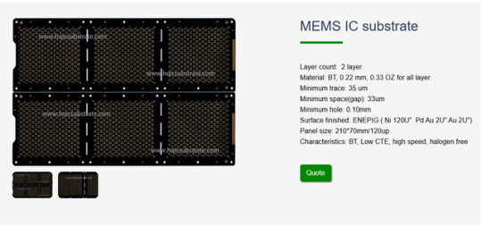
MEMS IC substrate
Layer count: 2 layer Material: BT, 0.22 mm, 0.33 OZ for all layer Minimum trace: 35 um Minimum space(gap): 33um Minimum hole: 0.10mm Surface finished: ENEPIG ( Ni 120U" Pd Au 2U" Au 2U") Panel size: 210*70mm/120up Characteristics: BT, Low CTE, high speed, halogen free
0 notes
Text

SiP IC Substrate Manufacturing Comprehensive Guide (2025)
I. Introduction A. Overview of SiP Technology B. Importance of hashtag#IC Substrates in SiP Packaging C. Purpose and Scope of the Guide II. Fundamentals of hashtag#SiP IC Substrate Manufacturing A. Definition and Role of IC Substrates B. Key Components and Materials 1. Dielectric Materials 2. Conductive Layers 3. Solder Mask and Surface Finishes C. Types of IC Substrates 1. Organic Substrates 2. Ceramic Substrates III. hashtag#Manufacturing Process Overview A. Design and Prototyping 1. hashtag#Substrate Layout Design 2. Simulation and Testing B. Material Preparation 1. Raw Material Selection 2. Pre-treatment Processes C. Substrate Fabrication Steps 1. Layer Formation a. Lamination b. Etching 2. Via Formation a. Mechanical Drilling b. Laser Drilling 3. Metallization and Plating a. Copper Deposition b. Surface Finishes (e.g., ENIG, OSP) IV. Advanced Manufacturing Techniques A. High-Density Interconnect (hashtag#HDI) Technology B. Embedded Component Integration C. Multi-layer and 3D Substrate Fabrication V. Quality Control and Testing A. Inspection Methods 1. Optical Inspection 2. X-Ray Analysis for Hidden Defects B. Electrical Testing Procedures 1. Continuity and Isolation Tests 2. Signal Integrity Analysis VI. Challenges and Solutions in SiP IC Substrate Manufacturing A. Miniaturization and Density Challenges B. Thermal Management Solutions C. Cost-Effective Manufacturing Strategies VII. Future Trends in SiP IC Substrate Technology (2025 and Beyond) A. Innovations in Materials Science B. AI and Automation in Manufacturing Processes C. Sustainability and Eco-Friendly Practices VIII. Conclusion A. Summary of Key Points B. Outlook for the SiP IC Substrate Industry
1 note
·
View note
Text

Substrate-like PCB China
Layer count: 4 layer Material: BT, 0.38 mm, 0.33 OZ for all layer Minimum trace: 30 um Minimum space(gap): 30um Minimum hole: 0.10mm Surface finished: ENEPIG ( Ni 200U" Pd 2U" Au 2U") Panel size: 258*76mm/198up Characteristics: Low CTE, high speed, ENEPIG for bonding, BT raw material
1 note
·
View note
Text
A Comprehensive Guide to substrate-like PCB Technology
The growing landscape of electronic manufacturing means one thing, Printed Circuit Boards (PCB) have a demand for more and doing it faster, smaller and with the same performance; update electronics tech.
1 note
·
View note
Text
The Silent Enabler: How IC Substrates Power the Semiconductor Revolution
Breaking Down the IC Substrate Ecosystem
The global IC substrate market has transformed into a $14.6 billion industry (Yole Développement 2025), driven by three core technology segments:

Advanced Packaging Platforms
2.5D/3D IC substrates now enable 12-layer interposers with <1μm alignment precision
Fan-out wafer-level packaging (FOWLP) achieves 0.8μm line/space resolution
Heterogeneous integration substrates support 10+ chiplet configurations
Material Science Breakthroughs
Low-loss dielectrics (Dk<3.0 @ 100GHz) from 8 major chemical suppliers
Nanocomposite thermal interface materials with 15W/mK conductivity
Photosensitive dielectric films enabling 2μm laser patterning
Cutting-Edge Manufacturing Innovations
Leading manufacturers have deployed:
AI-Optimized Production
Neural networks reducing warpage by 40% through real-time parameter adjustment
Digital twin systems predicting yield with 98.7% accuracy
Automated optical inspection achieving 50 defects per billion opportunities
Sustainable Manufacturing
Closed-loop chemical recycling recovering 92% of process materials
Plasma treatment replacing chemical desmear in 35% of facilities
Waterless cleaning systems reducing H2O usage by 8,000 tons/month per fab
Transformative Applications
AI/ML Hardware
NVIDIA's Blackwell GPU platform uses IC substrates with:
8μm microbump pitch
16-layer build-up structure
3D through-silicon via (TSV) integration
Automotive Electronics
Tesla's Dojo 2 training system incorporates:
45μm coreless substrates
Embedded decoupling capacitors
10μm ultra-fine line circuitry
Emerging Technology Frontiers
Quantum Computing
Cryogenic substrates operating at 4K with:
Superconducting niobium interconnects
Quantum-limited loss dielectrics
Magnetic field shielding layers
Biomedical Interfaces
Neural implant substrates featuring:
500nm flexible polyimide circuits
Biocompatible gold metallization
10-year in-vivo stability
Frequently Asked Questions
Why are IC substrates crucial for chiplet designs?
They provide:
Known-good-die (KGD) testing infrastructure
Ultra-short inter-chiplet links (<100μm)
Thermal stress buffering between heterogeneous dies
How do IC substrates enable 6G communications?
Through:
Terahertz waveguides with 0.001dB/mm loss
Antenna-in-package integration
3D electromagnetic shielding structures
What's the roadmap for IC substrate technology?
Key milestones include:
2026: 1μm line/space volume production
2028: Photonic interposer commercialization
2030: Molecular-scale self-assembling substrates
1 note
·
View note