#Enosemi
Explore tagged Tumblr posts
Visit Tumblr Blog
Explore Tumblr blogs with no restrictions, modern design and the best experience.
Last Seen Tumblr Blogs


Fun Fact
In February 2021, Tumblr had 518.6 million blog accounts.
Text
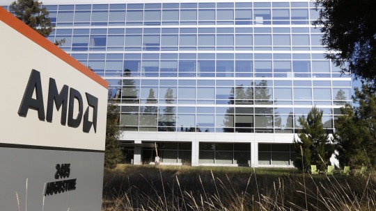
AMD buys silicon photonics startup Enosemi to gasoline its AI ambitions
AMD has acquired Enosemi, a startup designing customized supplies to help silicon photonics product growth. The phrases of the deal, introduced Wednesday, weren’t disclosed. Silicon photonics makes use of gentle — photons — to transmit information, providing a quicker and extra environment friendly different to conventional electrical communication. AMD and different chipmakers have proven an…
0 notes
Photo
AMD acquires Enosemi to enter the photonics race — chasing Nvidia into light-based interconnect technology Have you heard about AMD’s latest move into photonics? This strategic acquisition is designed to push AMD ahead in the race for next-generation interconnect tech, competing directly with Nvidia’s advancements. By purchasing Enosemi, a Silicon Valley company specializing in photonic integrated circuits, AMD is stepping into the future of chipmaking where light replaces electrons for faster, more efficient data transfer. Photonics, powered by light, is set to revolutionize high-speed communication within data centers and AI systems. This technology promises higher bandwidth and superior power efficiency—essential traits for advanced computing. AMD’s partnership with companies like GlobalFoundries and ongoing development in co-packaged optics highlight their commitment to pioneering this field. For tech enthusiasts and AI developers, AMD’s focus on photonics means exciting possibilities for faster and more scalable systems. Their goal? Build a full-stack AI solution that rivals Nvidia’s dominance, combining CPUs, GPUs, and now, light-based interconnects. Are you excited to see how photonics will shape the future of computing? What innovations in AI or data center hardware do you think will benefit most from this shift? Stay ahead of the curve and share your thoughts! #AI #Semiconductors #Photonics #DataCenters #FutureTech #Innovation #AMD #Nvidia #LightTech #AIHardware #Microchip #TechNews
0 notes
Text
AMD adquiere Enosemi y apuesta por la fotónica
AMD sigue reforzando su presencia en el competitivo mercado de la Inteligencia Artificial, y lo hace con un nuevo movimiento estratégico, la adquisición de Enosemi, una compañía especializada en fotónica del silicio y óptica avanzada. Aunque hasta ahora era un socio de desarrollo externo, ahora pasa a formar parte integral del ecosistema de AMD, aportando conocimientos clave en interconexión…

View On WordPress
0 notes
Photo

AMD Acquires Silicon Photonics Startup Enosemi to Boost its AI Ambitions
0 notes
Text
AMD announces the acquisition of enosemi to reinforce co-pack, AI
AMD announces the acquisition of enosemi to reinforce co-pack, AI Source link
0 notes
Text
AMD announces the acquisition of enosemi to reinforce co-pack, AI
AMD announces the acquisition of enosemi to reinforce co-pack, AI Source link
0 notes
Text
Photonic processor could enable ultrafast AI computations with extreme energy efficiency
New Post has been published on https://sunalei.org/news/photonic-processor-could-enable-ultrafast-ai-computations-with-extreme-energy-efficiency/
Photonic processor could enable ultrafast AI computations with extreme energy efficiency

The deep neural network models that power today’s most demanding machine-learning applications have grown so large and complex that they are pushing the limits of traditional electronic computing hardware.
Photonic hardware, which can perform machine-learning computations with light, offers a faster and more energy-efficient alternative. However, there are some types of neural network computations that a photonic device can’t perform, requiring the use of off-chip electronics or other techniques that hamper speed and efficiency.
Building on a decade of research, scientists from MIT and elsewhere have developed a new photonic chip that overcomes these roadblocks. They demonstrated a fully integrated photonic processor that can perform all the key computations of a deep neural network optically on the chip.
The optical device was able to complete the key computations for a machine-learning classification task in less than half a nanosecond while achieving more than 92 percent accuracy — performance that is on par with traditional hardware.
The chip, composed of interconnected modules that form an optical neural network, is fabricated using commercial foundry processes, which could enable the scaling of the technology and its integration into electronics.
In the long run, the photonic processor could lead to faster and more energy-efficient deep learning for computationally demanding applications like lidar, scientific research in astronomy and particle physics, or high-speed telecommunications.
“There are a lot of cases where how well the model performs isn’t the only thing that matters, but also how fast you can get an answer. Now that we have an end-to-end system that can run a neural network in optics, at a nanosecond time scale, we can start thinking at a higher level about applications and algorithms,” says Saumil Bandyopadhyay ’17, MEng ’18, PhD ’23, a visiting scientist in the Quantum Photonics and AI Group within the Research Laboratory of Electronics (RLE) and a postdoc at NTT Research, Inc., who is the lead author of a paper on the new chip.
Bandyopadhyay is joined on the paper by Alexander Sludds ’18, MEng ’19, PhD ’23; Nicholas Harris PhD ’17; Darius Bunandar PhD ’19; Stefan Krastanov, a former RLE research scientist who is now an assistant professor at the University of Massachusetts at Amherst; Ryan Hamerly, a visiting scientist at RLE and senior scientist at NTT Research; Matthew Streshinsky, a former silicon photonics lead at Nokia who is now co-founder and CEO of Enosemi; Michael Hochberg, president of Periplous, LLC; and Dirk Englund, a professor in the Department of Electrical Engineering and Computer Science, principal investigator of the Quantum Photonics and Artificial Intelligence Group and of RLE, and senior author of the paper. The research appears today in Nature Photonics.
Machine learning with light
Deep neural networks are composed of many interconnected layers of nodes, or neurons, that operate on input data to produce an output. One key operation in a deep neural network involves the use of linear algebra to perform matrix multiplication, which transforms data as it is passed from layer to layer.
But in addition to these linear operations, deep neural networks perform nonlinear operations that help the model learn more intricate patterns. Nonlinear operations, like activation functions, give deep neural networks the power to solve complex problems.
In 2017, Englund’s group, along with researchers in the lab of Marin Soljačić, the Cecil and Ida Green Professor of Physics, demonstrated an optical neural network on a single photonic chip that could perform matrix multiplication with light.
But at the time, the device couldn’t perform nonlinear operations on the chip. Optical data had to be converted into electrical signals and sent to a digital processor to perform nonlinear operations.
“Nonlinearity in optics is quite challenging because photons don’t interact with each other very easily. That makes it very power consuming to trigger optical nonlinearities, so it becomes challenging to build a system that can do it in a scalable way,” Bandyopadhyay explains.
They overcame that challenge by designing devices called nonlinear optical function units (NOFUs), which combine electronics and optics to implement nonlinear operations on the chip.
The researchers built an optical deep neural network on a photonic chip using three layers of devices that perform linear and nonlinear operations.
A fully-integrated network
At the outset, their system encodes the parameters of a deep neural network into light. Then, an array of programmable beamsplitters, which was demonstrated in the 2017 paper, performs matrix multiplication on those inputs.
The data then pass to programmable NOFUs, which implement nonlinear functions by siphoning off a small amount of light to photodiodes that convert optical signals to electric current. This process, which eliminates the need for an external amplifier, consumes very little energy.
“We stay in the optical domain the whole time, until the end when we want to read out the answer. This enables us to achieve ultra-low latency,” Bandyopadhyay says.
Achieving such low latency enabled them to efficiently train a deep neural network on the chip, a process known as in situ training that typically consumes a huge amount of energy in digital hardware.
“This is especially useful for systems where you are doing in-domain processing of optical signals, like navigation or telecommunications, but also in systems that you want to learn in real time,” he says.
The photonic system achieved more than 96 percent accuracy during training tests and more than 92 percent accuracy during inference, which is comparable to traditional hardware. In addition, the chip performs key computations in less than half a nanosecond.
“This work demonstrates that computing — at its essence, the mapping of inputs to outputs — can be compiled onto new architectures of linear and nonlinear physics that enable a fundamentally different scaling law of computation versus effort needed,” says Englund.
The entire circuit was fabricated using the same infrastructure and foundry processes that produce CMOS computer chips. This could enable the chip to be manufactured at scale, using tried-and-true techniques that introduce very little error into the fabrication process.
Scaling up their device and integrating it with real-world electronics like cameras or telecommunications systems will be a major focus of future work, Bandyopadhyay says. In addition, the researchers want to explore algorithms that can leverage the advantages of optics to train systems faster and with better energy efficiency.
This research was funded, in part, by the U.S. National Science Foundation, the U.S. Air Force Office of Scientific Research, and NTT Research.
0 notes
Text
Photonic processor could enable ultrafast AI computations with extreme energy efficiency
New Post has been published on https://thedigitalinsider.com/photonic-processor-could-enable-ultrafast-ai-computations-with-extreme-energy-efficiency/
Photonic processor could enable ultrafast AI computations with extreme energy efficiency

The deep neural network models that power today’s most demanding machine-learning applications have grown so large and complex that they are pushing the limits of traditional electronic computing hardware.
Photonic hardware, which can perform machine-learning computations with light, offers a faster and more energy-efficient alternative. However, there are some types of neural network computations that a photonic device can’t perform, requiring the use of off-chip electronics or other techniques that hamper speed and efficiency.
Building on a decade of research, scientists from MIT and elsewhere have developed a new photonic chip that overcomes these roadblocks. They demonstrated a fully integrated photonic processor that can perform all the key computations of a deep neural network optically on the chip.
The optical device was able to complete the key computations for a machine-learning classification task in less than half a nanosecond while achieving more than 92 percent accuracy — performance that is on par with traditional hardware.
The chip, composed of interconnected modules that form an optical neural network, is fabricated using commercial foundry processes, which could enable the scaling of the technology and its integration into electronics.
In the long run, the photonic processor could lead to faster and more energy-efficient deep learning for computationally demanding applications like lidar, scientific research in astronomy and particle physics, or high-speed telecommunications.
“There are a lot of cases where how well the model performs isn’t the only thing that matters, but also how fast you can get an answer. Now that we have an end-to-end system that can run a neural network in optics, at a nanosecond time scale, we can start thinking at a higher level about applications and algorithms,” says Saumil Bandyopadhyay ’17, MEng ’18, PhD ’23, a visiting scientist in the Quantum Photonics and AI Group within the Research Laboratory of Electronics (RLE) and a postdoc at NTT Research, Inc., who is the lead author of a paper on the new chip.
Bandyopadhyay is joined on the paper by Alexander Sludds ’18, MEng ’19, PhD ’23; Nicholas Harris PhD ’17; Darius Bunandar PhD ’19; Stefan Krastanov, a former RLE research scientist who is now an assistant professor at the University of Massachusetts at Amherst; Ryan Hamerly, a visiting scientist at RLE and senior scientist at NTT Research; Matthew Streshinsky, a former silicon photonics lead at Nokia who is now co-founder and CEO of Enosemi; Michael Hochberg, president of Periplous, LLC; and Dirk Englund, a professor in the Department of Electrical Engineering and Computer Science, principal investigator of the Quantum Photonics and Artificial Intelligence Group and of RLE, and senior author of the paper. The research appears today in Nature Photonics.
Machine learning with light
Deep neural networks are composed of many interconnected layers of nodes, or neurons, that operate on input data to produce an output. One key operation in a deep neural network involves the use of linear algebra to perform matrix multiplication, which transforms data as it is passed from layer to layer.
But in addition to these linear operations, deep neural networks perform nonlinear operations that help the model learn more intricate patterns. Nonlinear operations, like activation functions, give deep neural networks the power to solve complex problems.
In 2017, Englund’s group, along with researchers in the lab of Marin Soljačić, the Cecil and Ida Green Professor of Physics, demonstrated an optical neural network on a single photonic chip that could perform matrix multiplication with light.
But at the time, the device couldn’t perform nonlinear operations on the chip. Optical data had to be converted into electrical signals and sent to a digital processor to perform nonlinear operations.
“Nonlinearity in optics is quite challenging because photons don’t interact with each other very easily. That makes it very power consuming to trigger optical nonlinearities, so it becomes challenging to build a system that can do it in a scalable way,” Bandyopadhyay explains.
They overcame that challenge by designing devices called nonlinear optical function units (NOFUs), which combine electronics and optics to implement nonlinear operations on the chip.
The researchers built an optical deep neural network on a photonic chip using three layers of devices that perform linear and nonlinear operations.
A fully-integrated network
At the outset, their system encodes the parameters of a deep neural network into light. Then, an array of programmable beamsplitters, which was demonstrated in the 2017 paper, performs matrix multiplication on those inputs.
The data then pass to programmable NOFUs, which implement nonlinear functions by siphoning off a small amount of light to photodiodes that convert optical signals to electric current. This process, which eliminates the need for an external amplifier, consumes very little energy.
“We stay in the optical domain the whole time, until the end when we want to read out the answer. This enables us to achieve ultra-low latency,” Bandyopadhyay says.
Achieving such low latency enabled them to efficiently train a deep neural network on the chip, a process known as in situ training that typically consumes a huge amount of energy in digital hardware.
“This is especially useful for systems where you are doing in-domain processing of optical signals, like navigation or telecommunications, but also in systems that you want to learn in real time,” he says.
The photonic system achieved more than 96 percent accuracy during training tests and more than 92 percent accuracy during inference, which is comparable to traditional hardware. In addition, the chip performs key computations in less than half a nanosecond.
“This work demonstrates that computing — at its essence, the mapping of inputs to outputs — can be compiled onto new architectures of linear and nonlinear physics that enable a fundamentally different scaling law of computation versus effort needed,” says Englund.
The entire circuit was fabricated using the same infrastructure and foundry processes that produce CMOS computer chips. This could enable the chip to be manufactured at scale, using tried-and-true techniques that introduce very little error into the fabrication process.
Scaling up their device and integrating it with real-world electronics like cameras or telecommunications systems will be a major focus of future work, Bandyopadhyay says. In addition, the researchers want to explore algorithms that can leverage the advantages of optics to train systems faster and with better energy efficiency.
This research was funded, in part, by the U.S. National Science Foundation, the U.S. Air Force Office of Scientific Research, and NTT Research.
#ai#air#air force#Algorithms#applications#artificial#Artificial Intelligence#Astronomy#author#Building#Cameras#CEO#challenge#chip#chips#computation#computer#computer chips#Computer Science#Computer science and technology#computing#computing hardware#data#Deep Learning#devices#efficiency#Electrical engineering and computer science (EECS)#electronic#Electronics#energy
0 notes