#RF Antenna Module
Explore tagged Tumblr posts
Visit Tumblr Blog
Explore Tumblr blogs with no restrictions, modern design and the best experience.
Last Seen Tumblr Blogs


Fun Fact
69% of Tumblr users are millennials.
Text
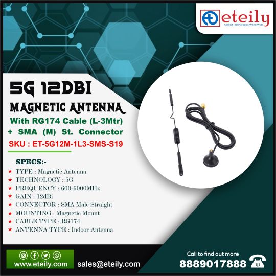
5G 12dBi Magnetic Antenna with RG174 Cable
A 5G 12dBi magnetic antenna is a type of antenna designed to enhance the performance of 5G wireless communication devices, such as routers, hotspots, or modems. Let's break down the key features:
5G: 5G is the fifth generation of wireless technology, which offers faster data speeds, lower latency, and greater capacity compared to previous generations (4G, 3G, etc.). The antenna is specifically designed to work with 5G networks and devices.
12dBi Gain: The "12dBi" figure refers to the antenna's gain, which is a measure of how much the antenna can increase the power of the signal it receives or transmits. A higher gain indicates better signal reception and transmission capabilities. In this case, a 12dBi gain suggests that this antenna can significantly boost the signal strength.
Magnetic Antenna: The term "Magnetic Antenna" indicates that the antenna can be attached to metal surfaces using a magnetic base. This feature provides flexibility in terms of placement and allows for easy positioning on metallic surfaces, like the roof of a car or a metal housing for a 5G device.
Magnetic antennas are often used in mobile applications or in scenarios where temporary or flexible mounting is required. This type of antenna is convenient because it can be easily installed and removed, making it suitable for mobile installations or where drilling holes or more permanent mounting solutions are not practical.
#rf antenna#RF Antennas#RF Antenna at Best Price in India#RF antenna system#radio frequency antenna#Best RF Solution Provider#RF Antenna Suppliers#Manufacturer of RF Antenna#rf antenna manufacturers in india#RF Antenna Manufacturer#RF Antenna Exporters#RF Antenna Latest Price#Wireless HF Antenna#RF Antenna Companies in India#Wholesaler of RF Antenna#RF Antenna Amplifier#RF Antenna Module#2.45 GHz Antenna Module#High Performance RF#Antennas for LoRa and Sigfox#Omni-directional SMD antennas#3.3GHz RF Antennas#RF & Microwave Antenna Manufacturers#Antenna manufacturers in Canada#RF Antenna manufacturers & suppliers - India#RF Antenna made in India#India telecom rf antenna#2.4ghz & 5ghz antenna#multiband antenna#telecom rf antenna products
0 notes
Text


sickest band merch ever
#i need to either get a standalone vhs player or a better way of transmitting signals than a rf modulator on an amplified tv antenna#so i can put this on my big crt
2 notes
·
View notes
Text
youtube
Panasonic: New Product Introduction: PAN1770 Series Bluetooth Low Energy RF Module
https://www.futureelectronics.com/m/panasonic . Panasonic PAN1770 Series is based on the Nordic nRF52840 single-chip controller that allows you to attach an external antenna via uFL. With the Cortex®-M4F processor, 256 kB RAM, and the built-in 1 MB flash memory, the PAN1770 Series can easily be used in standalone mode, eliminating the need for an external processor saving complexity, space, and cost. https://youtu.be/8Ur-bFMieHw
#Panasonic#PAN1770#Bluetooth Low Energy#RF Module#Nordic nRF52840#single-chip controller#external antenna#uFL#Bluetooth 5.3#LE 2M PHY#LE-coded PHY#Cortex-M4F processor#256 kB RAM#Panasonic single-chip controller#Youtube
0 notes
Text


Twin Famicom
NES with internal Disk system from Sharp
The Twin Famicom is a video game console system that was produced by Sharp Corporation in 1986 (Juli 1) and was only released in Japan. It is a licensed Nintendo product that combines the Famicom (NES) and the Famicom Disk System into a single piece of hardware.
The essential parts of the Twin Famicom include a 60-pin socket for Famicom cartridges and a socket for Disk System disks. The player could switch between the two media types with a switch – cassette "カセット" or disk "ディスク" The Twin Famicom is fully compatible with the NES and can handle accessories made for the NES (e.g. Beam Gun). But there is also an extra port on the Twin Famicom. This allows a 'regular' Famicom to use the Twin Famicom's disk drive.
The original Famicom only has one color combination, and the Twin Famicom was initially sold in two colors: red with black highlights (AN-500R), and black with red highlights (AN-500B). A second version of the system was released in 1987 with a slightly different case design, turbo controllers, and two different color schemes; black with green highlights (AN-505-BK) and red with beige highlights (AN-505-RD).
Like the Famicom, the Twin Famicom uses NTSC but with an AV output rather than an RF modulator with an RCA connector for composite video and mono audio, allowing for greater audiovisual quality on TVs and monitors with such inputs. An external RF modulator is bundled with the unit for connection through a TV's antenna/cable input. The two gamepads are hardwired into the console, so they cannot be disconnected.
More info:
https://ultimatepopculture.fandom.com/wiki/Twin_Famicom
#nintendo#famicom#twin famicom#sharp#nintendo disk system#retrogaming#retro gaming#nes#retro computing#retrocomputing#80s#80s computer#japan only
19 notes
·
View notes
Text
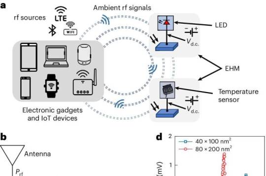
Battery-free technology can power electronic devices using ambient radiofrequency signals
Ubiquitous wireless technologies like Wi-Fi, Bluetooth, and 5G rely on radio frequency (RF) signals to send and receive data. A new prototype of an energy harvesting module—developed by a team led by scientists from the National University of Singapore (NUS)—can now convert ambient or "waste" RF signals into direct current (DC) voltage. This can be used to power small electronic devices without the use of batteries. RF energy harvesting technologies, such as this, are essential as they reduce battery dependency, extend device lifetimes, minimize environmental impact, and enhance the feasibility of wireless sensor networks and IoT devices in remote areas where frequent battery replacement is impractical. However, RF energy harvesting technologies face challenges due to low ambient RF signal power (typically less than -20 dBm), where current rectifier technology either fails to operate or exhibits a low RF-to-DC conversion efficiency. While improving antenna efficiency and impedance matching can enhance performance, this also increases on-chip size, presenting obstacles to integration and miniaturization.
Read more.
43 notes
·
View notes
Text

A mini GPS from uBlox with I2C and UART 🛰️📡🔧
The SAM-M8Q
is an entry-level 'all in one' GPS from uBlox - it comes with both UART and I2C interfaces plus a built-in antenna so it's ready to go 'out of the box.' It's also fairly small, so we decided to try and make a little breakout for it. It exposes both interfaces, but we expect most folks will like using the Stemma QT port for instant I2C interfacing. We gotta dig into uBlox's interface since we expect the I2C to be a little more complex than the PA1010 we've used.
#adafruit#gps#ublox#i2c#uart#sam-m8q#stemma#pa1010#electronics#gpsmodule#makerspace#hardwaredesign#embedded#opensourcetools#diyprojects#techinnovation#electronicsprojects#gpsbreakout#prototyping#smalldevices#sensorintegration#microcontroller#makersmovement
7 notes
·
View notes
Text
I saw @pc-98s do this and I had to try it for myself, can confirm it's very cool
(I forgot to add context that this is being streamed via an rf modulator through an antenna to the tv)
The girlies all together

(I forgot to turn oscilloscope for the photo lol)
23 notes
·
View notes
Text
Best Partner for Wireless Modules: A Comprehensive Antenna Selection Guide
n the field of wireless communication, antenna selection is crucial. It not only affects the coverage range and transmission quality of signals but also directly relates to the overall performance of the system. Among various wireless modules, finding the right antenna can maximize their potential, ensuring stable and efficient data transmission.
When designing wireless transceiver devices for RF systems, antenna design and selection are essential components. A high-quality antenna system can ensure optimal communication distances. Typically, the size of antennas of the same type is proportional to the wavelength of the RF signal; as signal strength increases, the number of required antennas also grows.
Antennae can be categorized as internal or external based on their installation location. Internal antennas are installed within the device, while external antennas are mounted outside.
In situations where space is limited or there are multiple frequency bands, antenna design becomes more complex. External antennas are usually standard products, allowing users to simply select the required frequency band without needing additional tuning, making them convenient and easy to use.
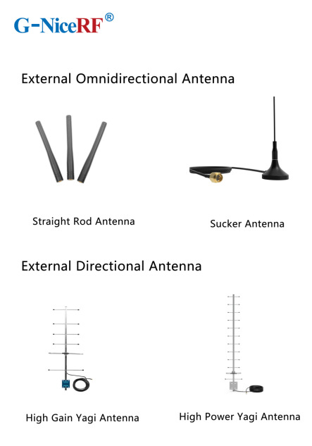
What are the main types of antennas?
External Antennas: These antennas can be classified into omnidirectional antennas and directional antennas based on the radiation pattern.
Internal Antennas: These antennas refer to antennas that can be placed inside devices.
Omnidirectional Antennas: These antennas radiate signals uniformly in the horizontal plane, making them suitable for applications that require 360-degree coverage, such as home Wi-Fi routers and mobile devices.
Directional Antennas: These antennas have a high emission and reception strength in one or more specific directions, while the strength is minimal or zero in others. Directional antennas are primarily used to enhance signal strength and improve interference resistance.
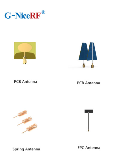
PCB Antennas: These antennas are directly printed on the circuit board and are suitable for devices with limited space, commonly used in small wireless modules and IoT devices.
FPC Antennas: FPC antennas are flexible printed circuit antennas that are lightweight, efficient, and easy to integrate.
Concealed Antennas: Designed for aesthetic purposes, concealed antennas can be hidden within devices or disguised as other objects, making them suitable for applications where appearance is important without compromising signal quality.
Antenna Selection Guide
When selecting the appropriate antenna for a communication module, it's essential to first determine whether to use an internal or external antenna based on the module's structure.
External Antennas: These antennas offer high gain, are less affected by the environment, and can save development time, but they may take up space and impact the product's aesthetics.
Internal Antennas: These have relatively high gain and are installed within the device, maintaining a clean and appealing exterior.
Sucker Antennas: These provide high gain and are easy to install and secure.
Copper Rod Sucker Antennas: Made from large-diameter pure copper radiators, these are highly efficient with a wide bandwidth.
Rubber Rod Antennas: Offer moderate gain at a low cost.
Fiberglass Antennas: Suitable for harsh environments and ideal for long-distance signal

External Directional Antennas
Typically used in environments with long communication distances, small signal coverage areas, and high target density.
Panel Antennas have high efficiency, are compact, and easy to install, while considering the impact of gain and radiation area Yagi Antennas offer very high gain, are slightly larger, and have strong directionality, making them suitable for long-distance signal transmission; however, attention must be paid to the antenna's orientation during use
Internal Antenna Selection
Most internal antennas are affected by environmental factors and may require custom design or impedance matching
Spring Antennas are cost-effective but have low gain and narrow bandwidth, often requiring tuning for good matching when installed Ceramic Patch Antennas occupy minimal space and perform well, but have a narrow bandwidth
For details, please click:https://www.nicerf.com/products/ Or click:https://nicerf.en.alibaba.com/productlist.html?spm=a2700.shop_index.88.4.1fec2b006JKUsd For consultation, please contact NiceRF (Email: [email protected]).
2 notes
·
View notes
Text
The People have spoken,
JermaTV is go. If anyone is interested/has technical questions feel free to ask but I’ll basically be modifying a composite TV RF modulator to be amplified slightly through an LNA board and out into a dummy load/highly non-efficient antenna. (I’ll play with power levels and see what the best output I can get is while following local regulations)
As far as what I’ll actually broadcast, please send me your favourite jerma moments™ and I’ll broadcast it on air / see if I could make a YouTube video out of it if you guys want.
#jerma#jerma tv#ham radio#amateur radio#amateurradio#amateur television#196#jerma985#electronics#electrical engineering
19 notes
·
View notes
Text
This FS1000A 433mHz Tx & Rx RF Module is a Compact, Economic and easy to use wireless RF module with both transmitter and receiver. The module operates at 433MHz and could communicate upto a range of 100 meters with proper antenna design. Practically with normal antenna it could cover distance of 20-50 meters. It can transmit at a speed of 1Kbps to 10Kbps and is easy to use with microcontrollers like Arduino, PIC, AVR etc..
5 notes
·
View notes
Text
Flip Chip Substrate Market : Global Trends and Forecast (2025 - 2032)

Global Flip Chip Substrate Market size was valued at US$ 8,730 million in 2024 and is projected to reach US$ 15,670 million by 2032, at a CAGR of 8.7% during the forecast period 2025-2032.
Flip chip substrates are critical components in semiconductor packaging, acting as miniature printed circuit boards (PCBs) that facilitate electrical connections between integrated circuits (ICs) and external circuitry. Unlike conventional PCBs, these substrates are designed to accommodate flip chip bonding, where ICs are mounted upside-down and connected directly to the substrate using solder bumps. Key materials used include ceramic, silicon, and organic substrates, each offering distinct advantages in thermal management and signal integrity.
Growth in the market is driven by rising demand for advanced semiconductor packaging solutions, particularly in high-performance computing (HPC), artificial intelligence (AI), and 5G applications. However, supply chain disruptions and fluctuating raw material costs pose challenges. Leading companies like Samsung Electronics, ASE Group, and Ibiden are investing in substrate technology to address the demand for finer pitch designs and improved thermal performance.
Get Full Report : https://semiconductorinsight.com/report/flip-chip-substrate-market/
MARKET DYNAMICS
MARKET DRIVERS
Growing Demand for High-Performance Computing Accelerates Flip Chip Adoption
The surging adoption of flip chip substrates is directly tied to explosive growth in high-performance computing applications from data centers to artificial intelligence. As computing architectures require higher bandwidth and lower latency, flip chip packaging provides superior electrical performance compared to wire bonding – achieving up to 40% reduction in signal delay while enabling higher pin counts. Leading semiconductor firms increasingly favor flip chip designs for advanced CPUs, GPUs, and AI accelerators where thermal management and interconnect density are critical. The market for AI chips alone is projected to expand at 35% CAGR through 2030, creating sustained demand for high-density flip chip substrates capable of supporting next-generation silicon.
5G Infrastructure Rollout Driving Advanced Packaging Requirements
Global 5G network deployments are creating ripple effects across semiconductor packaging, with flip chip substrates becoming essential for RF front-end modules and base station processors. These applications require packaging that minimizes parasitic effects while handling high-frequency signals – precisely where flip chip technology excels. As telecom operators invest over $250 billion annually in 5G infrastructure, substrate manufacturers are seeing unprecedented demand for low-loss dielectric materials and precision bumping technologies. The transition to mmWave frequencies in particular favors flip chip’s superior electrical characteristics, making it the packaging method of choice for next-generation wireless components.
➤ For instance, recent designs for 64T64R massive MIMO antennas now incorporate flip chip substrates exclusively to meet stringent RF performance requirements while minimizing footprint.
Furthermore, the automotive sector’s push toward autonomous driving systems represents another major growth vector. Advanced driver assistance systems (ADAS) relying on high-performance vision processors and radar modules increasingly adopt flip chip packaging to meet automotive-grade reliability standards while handling complex sensor fusion workloads.
MARKET RESTRAINTS
Complex Manufacturing Processes Constrain Market Expansion
While flip chip technology offers performance advantages, its manufacturing complexity presents significant barriers to adoption. The substrate fabrication process involves over 30 distinct production steps, from ultra-fine line patterning to precision bump placement, requiring specialized equipment with tight process controls. This complexity directly impacts yields and production costs, with defect rates in advanced substrates potentially reaching 15-20% for new process nodes. Many mid-tier semiconductor firms find the capital expenditure requirements prohibitive – a single bumping line can exceed $50 million in equipment investments.
Other Critical Challenges
Thermal Management Limitations Heat dissipation becomes increasingly problematic as flip chip densities rise. While solder bumps provide electrical connections, they create thermal resistance that can reduce chip reliability. Current substrate designs struggle to handle power densities exceeding 100W/cm² – a threshold being approached by next-generation AI accelerators and high-performance processors.
Material Compatibility Issues The coefficient of thermal expansion (CTE) mismatch between silicon dies and organic substrates remains an ongoing engineering challenge. Without perfect CTE matching, temperature cycling induces mechanical stress that can lead to solder joint failures and reduced product lifespan, particularly in automotive and industrial applications.
MARKET OPPORTUNITIES
Emerging 3D IC Technologies Create New Substrate Demand
The semiconductor industry’s shift toward 3D integration presents transformative opportunities for flip chip substrate providers. Advanced packaging architectures like chip-on-wafer-on-substrate (CoWoS) and integrated fan-out (InFO) require sophisticated interposers and redistribution layers that leverage flip chip technologies. As foundries invest heavily in 3D IC capabilities – with one leading player committing $30+ billion to advanced packaging R&D – substrate manufacturers able to deliver fine-pitch interconnects below 10μm stand to capture substantial market share.
Material Innovations Open New Application Verticals
Breakthroughs in substrate materials are expanding flip chip applications into previously inaccessible markets. Novel glass-based substrates demonstrate 50% lower signal loss compared to traditional organic materials while offering superior dimensional stability. These characteristics make them ideal for millimeter-wave automotive radar and high-frequency communications equipment. Similarly, developments in embedded passive components allow substrate manufacturers to integrate capacitors and inductors directly into the package, reducing board space requirements and improving electrical performance for IoT and mobile devices.
MARKET CHALLENGES
Geopolitical Factors Disrupt Supply Chain Stability
The flip chip substrate market faces growing uncertainty from trade restrictions and export controls affecting critical materials. Specialty resins and copper-clad laminates originating from specific regions now face 15-20% tariff premiums, increasing manufacturing costs across the supply chain. Furthermore, restrictions on advanced packaging equipment exports threaten to create technological bottlenecks, potentially delaying next-generation substrate development for non-approved regions.
Other Pressing Concerns
Workforce Development Lagging The industry faces an acute shortage of process engineers skilled in advanced substrate manufacturing techniques. With less than 30 accredited programs worldwide focused on semiconductor packaging, companies struggle to staff new production lines, slowing capacity expansion efforts despite strong demand.
Environmental Compliance Costs Stricter regulations on hazardous materials used in substrate fabrication, particularly concerning lead-free solder alternatives and solvent recovery, are adding 5-7% to production costs. These requirements vary significantly by region, complicating global manufacturing strategies for substrate suppliers.
FLIP CHIP SUBSTRATE MARKET TRENDS
Growing Demand for High-Performance Computing to Drive Market Expansion
The global flip chip substrate market is witnessing robust growth due to increasing demand for high-performance computing (HPC) applications in artificial intelligence, cloud computing, and data centers. Flip chip technology provides superior electrical performance compared to traditional wire bonding, offering higher signal density and better thermal dissipation. With semiconductor packaging evolving toward smaller form factors and higher power efficiency, flip chip substrates have become critical for advanced integrated circuits (ICs), CPUs, and GPUs. The market is projected to grow at a CAGR of over 6% from 2024 to 2032, driven by the semiconductor industry’s shift toward miniaturization and improved performance.
Other Trends
Advancements in Packaging Technologies
The growing adoption of fan-out wafer-level packaging (FOWLP) and 2.5D/3D IC packaging is influencing the flip chip substrate market, as these technologies require high-density interconnects for improved performance. Manufacturers are focusing on developing substrates with finer pitch capabilities and enhanced thermal management to meet the demands of advanced semiconductor nodes. Additionally, the rise of heterogeneous integration in chiplet-based designs is accelerating demand for flip chip substrates that can support multiple dies in a single package.
Increasing Investments in Electric Vehicles and 5G Infrastructure
The automotive and telecommunications sectors are emerging as key growth drivers for flip chip substrates, particularly with the rapid expansion of electric vehicles (EVs) and 5G networks. Flip chip technology is extensively used in power electronics for EV battery management systems (BMS) and ADAS applications, where thermal performance and reliability are critical. Meanwhile, 5G infrastructure development has heightened demand for high-frequency flip chip substrates in RF components, as they enable better signal integrity and power efficiency compared to conventional wire-bonded packages.
COMPETITIVE LANDSCAPE
Key Industry Players
Technological Innovation and Strategic Expansions Drive Market Competition
The global flip chip substrate market exhibits a semi-consolidated competitive structure, with established semiconductor manufacturers and substrate specialists vying for market share. Samsung Electronics and ASE Group emerge as dominant players, leveraging their vertical integration capabilities and extensive manufacturing footprints across Asia and North America. Samsung’s leadership stems from its advanced packaging solutions for memory and logic devices, while ASE maintains strength through its comprehensive flip chip packaging services.
Japanese firms Ibiden and SHINKO command significant market positions due to their expertise in high-density interconnect (HDI) substrates and ceramic-based solutions. These companies benefit from strong relationships with automotive and high-performance computing clients, with Ibiden securing numerous design wins for advanced chiplet packaging applications.
Several players are actively expanding production capacity to meet growing demand. Unimicron recently announced a $1.2 billion investment to expand its substrate manufacturing facilities in Taiwan, while Kinsus Interconnect Technology is increasing its focus on advanced substrate technologies for artificial intelligence processors. Meanwhile, European supplier AT&S is strengthening its position through strategic technology partnerships and new manufacturing sites in Southeast Asia.
The competitive intensity is further heightened by Chinese players like Zhen Ding Technology and Shennan Circuit, who are rapidly catching up technologically while competing aggressively on price. These companies benefit from government subsidies and growing domestic demand, posing both challenges and opportunities for established market leaders.
List of Key Flip Chip Substrate Companies Profiled
Samsung Electronics (South Korea)
ASE Group (Taiwan)
Ibiden (Japan)
SHINKO (Japan)
Unimicron (Taiwan)
Kinsus Interconnect Technology (Taiwan)
AT&S (Austria)
Kyocera (Japan)
Nan Ya PCB (Taiwan)
Zhen Ding Technology (China)
Shennan Circuit (China)
KLA (U.S.)
LG InnoTek (South Korea)
Daeduck Electronics (South Korea)
Segment Analysis:
By Type
Ceramic Substrate Dominates the Market Due to Superior Thermal Conductivity and Reliability
The market is segmented based on type into:
Ceramic Substrate
Subtypes: Alumina, Aluminum Nitride, and others
Silicon Substrate
Subtypes: Silicon Interposer, Silicon Wafer, and others
Others
By Application
Integrated Circuit Segment Leads Due to High Demand for Compact Electronics and Advanced Packaging
The market is segmented based on application into:
Integrated Circuit
CPU
Graphics Processing Unit
Others
By End-User Industry
Consumer Electronics Drives Market Growth with Increasing Adoption of Smart Devices
The market is segmented based on end-user industry into:
Consumer Electronics
Automotive
Telecommunications
Industrial
Aerospace & Defense
Healthcare
By Technology
Thermal Compression Bonding Technology Gains Traction for High-Density Packaging
The market is segmented based on technology into:
Mass Reflow
Thermal Compression Bonding
Others
Regional Analysis: Flip Chip Substrate Market
North America The North American flip chip substrate market is driven predominantly by the semiconductor industry’s strong presence and technological advancements in the U.S. and Canada. The region benefits from robust R&D investments, particularly in high-performance computing (HPC) and artificial intelligence (AI) applications, which demand advanced flip chip substrates. Major semiconductor players and packaging firms, such as Intel and ASE Group subsidiaries, are expanding their substrate manufacturing capabilities to accommodate next-generation designs. Additionally, government-backed initiatives, including the CHIPS and Science Act, which allocates $52 billion for semiconductor research and production, further propel market growth. However, the shift toward advanced substrates like silicon interposers presents challenges in terms of rising production costs.
Europe Europe emphasizes sustainable semiconductor manufacturing and technological innovation, which shapes the flip chip substrate market. Countries such as Germany, France, and the Netherlands are investing heavily in automotive and industrial IoT applications, where flip chip substrates provide superior thermal and electrical performance. The European semiconductor ecosystem, supported by companies including Infineon and STMicroelectronics, contributes to steady demand. However, reliance on Asian substrate suppliers and supply chain disruptions due to geopolitical tensions limit rapid expansion. Compliance with stringent EU environmental regulations further influences substrate material choices, with a shift toward lead-free and halogen-free alternatives gaining traction.
Asia-Pacific As the dominant region in the flip chip substrate market, Asia-Pacific accounts for over 60% of global production and consumption, led by semiconductor powerhouses China, Japan, South Korea, and Taiwan. Taiwan, home to major players like Unimicron and Nan Ya PCB, remains a hub for high-density flip chip substrate manufacturing. China’s aggressive push toward semiconductor self-sufficiency, backed by government subsidies, is increasing domestic substrate production. Japan and South Korea specialize in high-end substrates for memory and logic applications, catering to industry giants such as Samsung Electronics and SK Hynix. Despite cost-sensitive demand in emerging Southeast Asian markets, advancements in packaging technologies sustain steady adoption.
South America The flip chip substrate market in South America is nascent but growing, predominantly fueled by Brazil’s automotive and consumer electronics sectors. However, limited semiconductor fabrication capabilities and reliance on imports hinder market expansion. Economic instability in key countries like Argentina further restricts large-scale investments in advanced packaging solutions. Nonetheless, increasing demand for IoT devices and telecommunications infrastructure presents long-term opportunities for incremental growth.
Middle East & Africa This region exhibits emerging demand for flip chip substrates, primarily driven by telecommunications and data center expansions in the UAE, Saudi Arabia, and South Africa. While the lack of indigenous semiconductor manufacturing limits immediate adoption, partnerships with global substrate suppliers are gradually improving accessibility. Government-led tech diversification initiatives, such as Saudi Arabia’s Vision 2030, could accelerate regional growth, though geopolitical and logistical challenges remain obstacles.
Get A Detailed Sample Report : https://semiconductorinsight.com/download-sample-report/?product_id=97593
Report Scope
This market research report provides a comprehensive analysis of the Global Flip Chip Substrate Market, covering the forecast period 2025–2032. It offers detailed insights into market dynamics, technological advancements, competitive landscape, and key trends shaping the industry.
Key focus areas of the report include:
Market Size & Forecast: Historical data and future projections for revenue, unit shipments, and market value across major regions and segments. The Global Flip Chip Substrate market was valued at USD million in 2024 and is projected to reach USD million by 2032.
Segmentation Analysis: Detailed breakdown by product type (Ceramic Substrate, Silicon Substrate, Others), application (Integrated Circuit, CPU, Graphics Processing Unit, Others), and end-user industry to identify high-growth segments and investment opportunities.
Regional Outlook: Insights into market performance across North America, Europe, Asia-Pacific, Latin America, and the Middle East & Africa, including country-level analysis where relevant. Asia-Pacific remains the dominant market due to semiconductor manufacturing concentration.
Competitive Landscape: Profiles of leading market participants including Samsung Electronics, ASE Group, SHINKO, Ibiden, and Unimicron, including their product offerings, R&D focus, and recent developments such as mergers and acquisitions.
Technology Trends & Innovation: Assessment of emerging technologies in semiconductor packaging, advanced substrate materials, and evolving industry standards like heterogeneous integration.
Market Drivers & Restraints: Evaluation of factors driving market growth including demand for high-performance computing and advanced packaging, along with challenges like supply chain constraints and material shortages.
Stakeholder Analysis: Insights for semiconductor manufacturers, substrate suppliers, foundries, OSATs, and investors regarding the evolving ecosystem and strategic opportunities.
Primary and secondary research methods are employed, including interviews with industry experts, data from verified sources, and real-time market intelligence to ensure the accuracy and reliability of the insights presented.
Related Reports :
https://semiconductorinsight.com/report/global-gesture-sensor-market/
https://semiconductorinsight.com/report/iris-recognition-access-control-system-market/
Contact us:
+91 8087992013
0 notes
Text
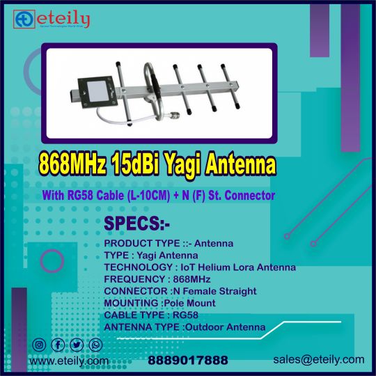
GSM 15dBi Yagi Antenna with RG58 Cable (L-10CM) + N (F) St. Connector
ETEILY Manufactures Yagi Antennas with good performance that comes handy, suitably working in all environment conditions.Our directional antennas are both suited for domestic as well as commercial applications.
Robust Mechanical design
High Gain
Good Signal Reception
Better Signal to Noise ratio
#Yagi–Uda antenna#Yagi antenna#Yagi beam antenna#rf antenna#RF Antennas#RF Antenna at Best Price in India#RF antenna system#radio frequency antenna#Best RF Solution Provider#RF Antenna Suppliers#Manufacturer of RF Antenna#rf antenna manufacturers in india#RF Antenna Manufacturer#RF Antenna Exporters#RF Antenna Latest Price#Wireless HF Antenna#RF Antenna Companies in India#Wholesaler of RF Antenna#RF Antenna Amplifier#RF Antenna Module#2.45 GHz Antenna Module#High Performance RF#Antennas for LoRa and Sigfox#Omni-directional SMD antennas#3.3GHz RF Antennas#RF & Microwave Antenna Manufacturers#Antenna manufacturers in Canada#RF Antenna manufacturers & suppliers - India#RF Antenna made in India#India telecom rf antenna
0 notes
Text
inventing new awful ways to watch tv by broadcasting youtube from a shitty rabbit ear antenna connected to an RF modulator
5K notes
·
View notes
Text
NB-IoT Equipment antenna electrostatic surge protection scheme

Narrowband Internet of Things (NB-IoT) Technology Overview
NB-IoT (Narrow Band Internet of Things) is a wireless communication technology designed to provide low-power consumption, wide coverage, and high-reliability connectivity for IoT devices. As a variant of LTE (Long Term Evolution), it is specifically optimized to support large-scale low-power, low-speed IoT communication requirements.
Key Characteristics of NB-IoT
l Low Power Consumption:NB-IoT employs optimized RF design and narrowband communication technology, enabling devices to operate in low-power modes for extended periods and significantly extending battery life.
l Wide Coverage:Leveraging existing LTE infrastructure, NB-IoT achieves broader coverage, including indoor and underground environments.
l High Reliability:Through techniques such as retransmission mechanisms and error verification, NB-IoT ensures reliable data transmission, maintaining connectivity even in poor signal conditions.
l Low Cost:By utilizing the existing LTE network, NB-IoT eliminates the need for additional infrastructure investment, resulting in low deployment and maintenance costs.
l Applications
NB-IoT is widely used in IoT fields such as smart cities, smart homes, smart meters, and environmental monitoring. It provides reliable connectivity for various IoT devices, facilitating large-scale deployment and cost-effective management of IoT applications.
Necessity of ESD/EOS Protection for NB-IoT Antennas
NB-IoT devices are deployed in diverse environments (indoor and outdoor), making antenna electrostatic surge protection critical:
l ESD Risks:Static electricity can accumulate between the device and antenna, causing electrostatic discharge that may damage equipment.
l Surge Risks:Outdoor environments are susceptible to unstable weather (e.g., lightning strikes), which can induce electrical surges, damaging equipment and systems.
l Solution:Install static surge protection components at the antenna interface to clamp overvoltage and mitigate surge-induced damage. Shanghai Leiditech offers specialized protection solutions for this scenario.
Shanghai Leiditech Protection Recommendations
Solution Advantages
Designed for NB-IoT antenna interfaces, the solution features ultra-low capacitance to ensure signal integrity while providing robust ESD/EOS protection.
Component Selection Guide
ESD Diodes (Based on Module Voltage):
3.3V Systems: ULC3311CDN (ultra-low junction capacitance)
5V Systems: ULC0511CDN30 (contact discharge: 30kV; air discharge: 30kV)
Surge Protection (for IEC 61000–4–5 Compliance):
Front-end GDT devices: SMD4532–090NF or 2R090–5 series


Leiditech Electronics is committed to becoming a leading brand in electromagnetic compatibility (EMC) solutions and component supply. We offer a wide range of products, including ESD, TVS, TSS, GDT, MOV, MOSFET, Zener diodes, and inductors. With an experienced R&D team, we provide personalized customization services to deliver the highest quality EMC solutions tailored to our customers’ needs.
If you’d like to learn more or have any questions, don’t hesitate to reach out:
Visit us at [en.leiditech.com]
NBIoT #IoTProtection #ESDProtection #SurgeProtection #SmartDevices #IoTSecurity #IndustrialIoT #ElectronicsDesign #EMC #Leiditech #SmartSolutions #5GReady #LowPowerWideArea #TechInnovation
0 notes
Text
Twin Famicom (NES model by Sharp)
The Twin Famicom is a video game console system that was produced by Sharp Corporation in 1986 (Juli 1) and was only released in Japan. It is a licensed Nintendo product that combines the Famicom (NES) and the Famicom Disk System into a single piece of hardware.
The essential parts of the Twin Famicom include a 60-pin socket for Famicom cartridges and a socket for Disk System disk cards. The player could switch between the two media types with a switch – cassette "カセット" or disk "ディスク" The Twin Famicom is fully compatible with the NES and can handle accessories made for the NES (e.g. Beam Gun). But there is also an extra port on the Twin Famicom. This allows a 'regular' Famicom to use the Twin Famicom's disk drive.

The original Famicom only has one color combination, and the Twin Famicom was initially sold in two colors: red with black highlights (AN-500R), and black with red highlights (AN-500B). A second version of the system was released in 1987 with a slightly different case design, turbo controllers, and two different color schemes; black with green highlights (AN-505-BK) and red with beige highlights (AN-505-RD).
Like the Famicom, the Twin Famicom uses NTSC but with an AV output rather than an RF modulator[2][3] with an RCA connector for composite video and mono audio, allowing for greater audiovisual quality on TVs and monitors with such inputs. An external RF modulator is bundled with the unit for connection through a TV's antenna/cable input. The two gamepads are hardwired into the console, so they cannot be disconnected. Source: Wiki NES models Check these out too if you are interested in retro computing


24 notes
·
View notes
Text
RF Test Equipment Market Size Ensuring Reliability in High-Frequency Communications
The RF Test Equipment Market Size is critical for validating the performance of wireless communication systems—including 5G, IoT networks, aerospace, defense, and automotive radar. With spectrum complexity increasing and RF devices integrating with digital processors, precise testing across frequencies, modulation schemes, and transmission standards is essential to ensure reliability, compliance, and security.
Market Size Research Future projects that global RF test equipment demand will reach USD 15.8 billion by 2030, growing at a CAGR of 6.7% between 2023 and 2030. Factors driving this growth include rapid global deployment of 5G infrastructure, expanding wireless device usage, and stringent regulatory standards.
Market Size Overview
RF test equipment encompasses a range of tools—signal generators, spectrum analyzers, vector signal analyzers, network analyzers, power meters, and communication testers—that verify signal integrity, receiver sensitivity, transmitter power, and RF chain performance. These instruments are essential during R&D, manufacturing validation, and routine field maintenance.
As devices like smartphones, IoT sensors, vehicle-to-everything (V2X) units, and network nodes become more complex, RF testing is moving toward automated, cloud-enabled, and AI-assisted solutions to support high-volume production and sustainable operation.
Key Drivers
1. 5G Rollout and Beyond
With the rollout of 5G and exploration of 6G, test instruments must support wide frequency bands, millimeter-wave testing, ultra-low latency metrics, and multi-antenna (MIMO) evaluation.
2. Growth of IoT and Connected Devices
The proliferation of IoT devices from home automation to industrial sensors is increasing the load on RF testing for Bluetooth, Wi-Fi, LoRa, NB-IoT, and cellular modules.
3. Automotive Radar & V2X Testing
Advanced driver-assistance systems (ADAS) and autonomous vehicles rely on radar and communication subsystems, increasing demand for precise RF field-testing equipment.
4. Regulatory and Compliance Testing
Equipment manufacturers must meet global standards for electromagnetic interference (EMI), wireless certification, and spectral compliance—driving the demand for EMI testing chambers, signal analyzers, and filters.
Market Size Segmentation
By Product Type:
Signal Generators
Spectrum Analyzers
Vector Signal Testers
Network Analyzers
Power Meters
Others (EMI Pre-compliance Tools)
By Frequency Range:
Below 3 GHz
3–6 GHz
Above 6 GHz (including mmWave)
By End User:
Telecommunication Infrastructure
Consumer Electronics
Aerospace & Defense
Automotive & Transportation
Industrial & Manufacturing
Research & Academic Institutions
Regional Overview
North America
Leading in test instrumentation adoption due to advanced 5G deployments, strong presence of OEMs, and robust R&D investment.
Europe
Market Size growth driven by 5G expansion, automotive radar development, and stringent certification processes in Germany, the UK, and France.
Asia-Pacific
The fastest-growing region, with China, Japan, South Korea, and India rapidly deploying 5G networks and scaling consumer electronics production.
Key Players
Major RF test equipment manufacturers are advancing into integrated software and AI-driven testing platforms:
Keysight Technologies
Rohde & Schwarz
National Instruments (NI)
Anritus Corporation
Tektronix (Fortive Corporation)
EXFO Inc.
Oscilent
VIAVI Solutions
LitePoint (Novanta)
Yokogawa Electric
These providers offer solutions ranging from lab-grade instrumentation to portable handheld testers and cloud-enabled automated test suites.
Trends to Watch
Cloud-Connected Test Labs: Remote calibration, automated reporting, and shared test infrastructure via cloud platforms.
AI-Enhanced Testing: Predictive fault detection and self-tuning instruments reduce cycle time and improve yield.
Portable RF Analyzers: Compact tools for field engineers testing base stations, towers, and broadcasting equipment.
Integrated IoT Testbeds: Platforms that combine RF testing with protocol analysis for IoT connectivity validation.
EMC/EMI Convergence: Multi-function analyzers covering both RF performance and EMC compliance testing.
Challenges
High Cost of Advanced Testers: Especially for mmWave and multi-antenna systems.
Complexity in Test Integration: Integrating RF test workflows with software and digital validation ecosystems.
Short Technology Lifecycles: Rapid need to update test equipment with new standards like 5G-Advanced and 6G.
Skilled Workforce Shortage: RF instrumentation prescribing domain knowledge is still rare.
Future Forecast
RF test platforms will evolve toward modular, scalable, and software-defined instruments compatible with automated production lines and remote management frameworks. The integration of edge-AI and digital twin-based test management will further accelerate deployment and reduce downtime.
Trending Report Highlights
Explore related sectors driving enhanced testing, connectivity, and automation:
USB Flash Drives Market Size
Bakery Release Agents Market Size
Circular Waterproof Connector Market Size
Capacitor Bank Controllers Substation Automation Market Size
Robotic Waste Sorting Market Size
Electromagnetic Compatibility (EMC) Filtration Market Size
Flash Charger Adapter Market Size
PM2.5 Sensor Market Size
Switched Capacitor Filter Market Size
Ultrasound Pulser IC Market Size
Pressfit Connectors Market Size
Sensor Signal Conditioner ICs Market Size
Waterproof LED Module Market Size
0 notes