#Rigid-Flex PCB Stackup
Explore tagged Tumblr posts
Visit Tumblr Blog
Explore Tumblr blogs with no restrictions, modern design and the best experience.
Last Seen Tumblr Blogs


Fun Fact
The Tumblr app for Google Glass was released on May 16, 2013.
Text
Rigid-Flex PCB Stackup
Discover the advanced capabilities of our rigid-flex PCB stackup at XPCB Limited, designed to meet the demands of modern electronic applications. Our innovative stackup combines the durability of rigid boards with the flexibility of flexible circuits, allowing for compact designs and enhanced performance in tight spaces. With superior signal integrity and reduced weight, our rigid-flex PCBs are ideal for a variety of industries, including aerospace, medical, and consumer electronics. For inquiries, please contact us at +86-136-3163-3671
0 notes
Text
Top-Tier PCB Fabrication Services for Every Industry
High-performance printed circuit boards (PCBs) continue growing across every industry. From consumer electronics to aerospace, medical devices to automotive systems, the quality of a PCB can determine the performance, efficiency, and durability of an entire product. That's why top-tier PCB fabrication services are more critical than ever — and why choosing the right PCB fabrication company can make or break your success.
At the heart of every advanced electronic product lies a well-engineered PCB. As a trusted PCB manufacturing company, our mission is to deliver high-quality, precision-fabricated PCBs that meet the specific needs of your project, no matter how simple or complex.
Precision Engineering for Maximum Performance
Our PCB fabrication services are built on a foundation of engineering excellence. We use state-of-the-art technology and a highly skilled team to produce PCBs that meet tight tolerances and rigorous quality standards. Whether you're working with a standard double-sided design or a multilayer, high-density interconnect (HDI) board, we have the capability to deliver with precision.
Key fabrication capabilities include:
Single, Double, and Multilayer PCBs
HDI and Rigid-Flex Boards
High-Frequency & High-Speed PCBs
Heavy Copper & Metal Core PCBs
Lead-Free & RoHS Compliant Options
Through Hole PCB Assembly and Surface Mount Technology (SMT)
Each board is fabricated using high-grade materials and strict process control to ensure superior reliability and performance in real-world applications. Whether you need quick turn PCB assembly services for a prototype or a full-scale production run, we’re ready to meet your deadline.
Serving a Broad Spectrum of Industries
What sets us apart as a full-service PCB manufacturing company is our versatility. We support customers across a wide range of industries, offering specialized expertise in each vertical:
Consumer Electronics – Smartphones, wearables, and smart appliances require compact, high-speed PCBs with impeccable performance.
Automotive – From powertrain systems to in-car infotainment, automotive electronics rely on durable, high-temperature-resistant boards.
Medical Devices – Life-saving equipment like imaging systems and portable monitors demand extreme precision and zero-defect standards.
Industrial Automation – PCBs for control systems, robotics, and sensors must withstand harsh environments and continuous operation.
Telecommunications – Our fabrication processes support high-frequency RF boards essential to telecom infrastructure and 5G devices.
Aerospace & Defense – We offer military-grade fabrication for mission-critical electronics with strict adherence to industry standards.
No matter your application, our team works closely with you to understand your technical requirements and deliver boards that exceed expectations.
Customized PCB Fabrication Solutions
Every project is unique, and we believe in delivering tailored solutions that align with your product's performance, budget, and production timeline. As an experienced PCB fabrication company, we provide comprehensive design-to-delivery support to streamline your workflow.
Whether you're at the prototyping stage or preparing for full-scale production, we offer:
Quick-Turn Prototyping
Small to High-Volume Production
Custom Stackups & Impedance Control
Material Selection Guidance
DFM (Design for Manufacturability) Feedback
Quick Turn PCB Assembly Services to accelerate product development
Our design support team is available to review your Gerber files, assist with layout optimization, and ensure that your design is perfectly matched to our manufacturing capabilities.
Uncompromised Quality and Certification Standards
Quality is non-negotiable. All our fabrication processes are governed by international standards and robust quality management systems. We conduct multi-stage inspections and automated optical testing (AOI) at every critical phase of production.
Certifications and quality assurances include:
ISO 9001:2015 Certified
IPC Class 2 & Class 3 Compliant
UL Certification
RoHS and REACH Compliance
Full Traceability of Materials and Processes
Whether it's high-volume orders or through hole PCB assembly projects with complex layouts, our goal is to deliver zero-defect PCBs that perform flawlessly in their intended environment, every single time.
Fast Turnaround and On-Time Delivery
In fast-moving markets, time-to-market is everything. That’s why we offer quick turn PCB assembly services with guaranteed lead times, giving you the flexibility to meet tight project deadlines without compromising on quality.
Our streamlined workflow, in-house capabilities, and experienced logistics team ensure that your PCBs are delivered on time and ready for assembly — whether you're local or overseas.
Your Trusted PCB Fabrication Partner
Partnering with us means more than just placing an order — it means gaining a dedicated team invested in your product’s success. As a full-service PCB fabrication company, our focus on innovation, precision, and customer service has made us a trusted name in the electronics manufacturing industry for startups, engineers, and Fortune 500 companies alike.
We invite you to experience the difference of working with a fabrication house that puts your needs first.
Let’s Build the Future Together
Ready to get started? Whether you have a complex multilayer board, a custom design requiring through hole PCB assembly, or need quick turn PCB assembly services, our expert team is here to help you move from concept to reality — faster and better than ever before.
Contact us today for a free quote or design consultation, and discover how a trusted PCB manufacturing company can elevate your next project.
Let me know if you'd like this adapted into a landing page, brochure copy, or SEO-optimized blog!
0 notes
Text
Exploring Rigid-Flexible Circuits: Advantages, Applications, and Design Considerations Rigid Flexible Circuits
Introduce the concept of rigid-flex circuits, highlighting their significance in modern electronics and their ability to combine the advantages of both rigid and flexible PCBs.Emphasize the importance of understanding the unique features and design considerations of rigid-flex circuits for various applications.
Section 1: What are Rigid-Flexible Circuits? Rigid Flexible CircuitsRigid Flexible Circuits
Define rigid-flex circuits as hybrid PCBs that incorporate both rigid and flexible substrates interconnected to form a single, integrated circuit.Explain the construction of rigid-flex circuits, including rigid sections for component mounting and flexible sections for bending and conforming to 3D shapes.
Section 2: Advantages of Rigid-Flexible Circuits: Rigid Flexible CircuitsRigid Flexible Circuits
Discuss the key advantages of using rigid-flex circuits over traditional rigid or flexible PCBs, such as:
Reduced assembly time and complexity by eliminating the need for connectors and interconnects.
Enhanced reliability and durability due to fewer solder joints and interconnection points.
Space savings and weight reduction in compact electronic devices, leading to improved design flexibility and performance.
Section 3: Applications of Rigid-Flexible Circuits: Rigid Flexible Circuits
Explore the diverse applications of rigid-flex circuits across various industries, including:
Wearable electronics (e.g., smartwatches, fitness trackers).
Medical devices and implantable electronics.
Aerospace and defense systems (e.g., avionics, unmanned aerial vehicles).
Automotive electronics (e.g., instrument clusters, infotainment systems).
Consumer electronics (e.g., smartphones, tablets, foldable displays).
Section 4: Design Considerations for Rigid-Flexible Circuits: Rigid Flexible Circuits
Provide guidelines and best practices for designing rigid-flex circuits, including:
Optimizing the layout and placement of rigid and flexible sections to minimize stress and strain during bending and flexing.
Selecting appropriate materials and stackup configurations to meet mechanical, thermal, and electrical performance requirements.
Considering factors such as bend radius, bend cycles, and dynamic flexing for long-term reliability and durability.
Section 5: Manufacturing Challenges and Solutions: Rigid Flexible Circuits
Discuss common manufacturing challenges associated with rigid-flex circuits, such as material compatibility, registration accuracy, and assembly processes.Offer solutions and strategies for overcoming these challenges, such as utilizing advanced manufacturing techniques, automation, and quality control measures.
Section 6: Future Trends and Developments: Rigid Flexible Circuits
Highlight emerging trends and developments in rigid-flex circuit technology, including:
Advancements in flexible substrate materials with improved mechanical properties and thermal stability.
Integration of additive manufacturing and 3D printing technologies for customized and complex rigid-flex designs.
Adoption of flexible hybrid electronics (FHE) concepts for seamless integration of sensors, actuators, and electronic components into flexible substrates.
Conclusion: Rigid Flexible Circuits
Summarize the key points discussed in the article about rigid-flex circuits and their importance in modern electronics.Encourage further exploration of rigid-flex circuit technology and collaboration with experienced PCB designers and manufacturers to leverage its benefits for innovative electronic products.
0 notes
Text
0 notes
Text
.
Rigid-Flex PCB: Revolutionizing Electronics with Flexibility and Rigidity
In the ever-evolving landscape of electronics, innovation often comes in the form of new materials and designs that push the boundaries of what is possible. Rigid-Flex PCB (Printed Circuit Board) is a prime example of such innovation, seamlessly combining the benefits of rigidity and flexibility to meet the demands of modern electronic devices. This hybrid construction has transformed the way electronic components are integrated, offering designers greater flexibility and versatility.
Understanding Rigid-Flex PCB: At its core, a Rigid-Flex PCB is a combination of rigid and flexible circuitry within a single board. It consists of both rigid sections, typically made of FR-4 material, and flexible sections, composed of polyimide or similar flexible substrates. This unique construction allows the board to bend or fold without compromising the integrity of the circuitry.
Versatility in Design: One of the primary advantages of Rigid-Flex PCB is its versatility in design. Traditional rigid boards are limited by their fixed shape, whereas flexible circuits can conform to non-planar surfaces. Rigid-Flex PCBs bridge this gap, offering designers the freedom to create 3D configurations that were once challenging or impossible with separate rigid and flexible boards.
Space Efficiency and Weight Reduction: The integration of rigid and flexible sections in a single board leads to enhanced space efficiency. Instead of using connectors and cables to link separate rigid and flexible boards, Rigid-Flex PCBs eliminate these additional components, reducing the overall size and weight of the electronic device. This is particularly beneficial in applications where size and weight constraints are critical factors.
Reliability and Durability: Rigid-Flex PCBs offer improved reliability compared to assemblies using connectors and cables. The elimination of interconnects reduces the points of failure, minimizing the risk of signal degradation, electrical noise, and mechanical wear. The seamless integration of rigid and flexible sections ensures durability, making Rigid-Flex PCBs suitable for applications subjected to repeated bending or flexing.
Complex Circuitry Integration: The combination of rigid and flexible sections facilitates the integration of complex circuitry within a compact space. Designers can strategically place rigid areas for components requiring stability and flexibility in sections that demand adaptability. This capability is especially advantageous in densely populated electronic devices where space optimization is critical.
Applications in Various Industries: Rigid-Flex PCB technology has found applications in a diverse range of industries. From aerospace and automotive to medical devices and consumer electronics, the adaptability of Rigid-Flex PCBs makes them suitable for numerous applications. In the automotive sector, for instance, Rigid-Flex PCBs are employed in airbag systems, control modules, and instrument clusters, benefiting from the space-saving and reliability features.
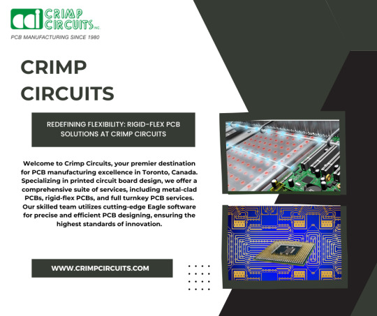
Challenges and Considerations: While Rigid-Flex PCBs offer significant advantages, their design and manufacturing present unique challenges. Designers must carefully consider factors such as material compatibility, bend radius, and layer stackup. Collaboration between electrical and mechanical engineers is crucial to ensure that the final design meets both electrical and mechanical requirements.
Conclusion: In conclusion, Rigid-Flex PCB technology represents a paradigm shift in the world of electronic design and manufacturing. Its ability to seamlessly blend rigidity and flexibility opens up new possibilities for compact, lightweight, and reliable electronic devices. As technology continues to advance, Rigid-Flex PCBs will likely play an increasingly pivotal role in shaping the future of electronic innovations, offering a harmonious blend of form and function in the realm of printed circuit boards.
For more details visit our website : www.crimpcircuits.com
#pcb manufacturing toronto#printed circuit board design#metal clad pcb#printed circuits#rigid flex pcb#full turnkey pcb services#turnkey pcb services#pcb parts#eagle software#pcb designing#flexible pcb#pcb assembly#printed circuit board manufacturers#pcb manufacturers in canada#circuit board manufacturers in canada#pcb quote#pcb prototype services in canada
0 notes
Text
Breakthrough Technologies: Exploring the Future of PCB Circuit Design
Printed circuit board (PCB) design is essential to the creation of cutting-edge electronic products in today’s continuously changing technological environment. Innovative PCB circuit design solutions are crucial as businesses and consumers want devices that are more complex and compact. This article examines the prospects for PCB circuit design and presents ground-breaking innovations that promise to transform the market.

Designing PCB Circuits: Its Importance
Recognising PCBs
The basis for electrical connections and the foundation for parts like resistors, capacitors, and integrated circuits, PCBs comprise the core of contemporary electronic gadgets. The functionality, dependability, and manufactureability of electronic devices are significantly influenced by the design and arrangement of these boards.
Demands of a Changing Industry
Electronic devices becoming smaller, more powerful, and feature-rich as technology develops. Due to this development, PCB designers are under more pressure to produce compact boards that can hold more components while ensuring ideal signal integrity and thermal management.
What a PCB Circuit Design Does
The process of designing a PCB circuit is laying out and connecting electronic components physically on a board. Electrical engineering, materials science, and manufacturing process knowledge are prerequisites. Effective PCB circuit design promotes reliable electronic device operation and transfer of signals while minimising electromagnetic interference.
PCB Circuit Design Development
From Traditional to Modern
PCB (Printed Circuit Board) Design has advanced significantly from its infancy. The placement of individual components on a board and their wiring together were traditionally done manually to construct PCBs. But technological developments have revolutionised this industry and improved its accuracy and efficiency.
CAD (Computer-Aided Design) introduction
In the field of PCB circuit design, the arrival of Computer-Aided Design (CAD) software has completely changed the game. Using CAD tools, engineers can digitally design, simulate, and test circuits, greatly decreasing the time and effort needed to create intricate PCB layouts.
Integration and Miniaturisation
The need for smaller and more potent electrical devices has increased dramatically as a result of the quick development of technology. Component integration and miniaturisation inside PCBs have resulted from this. Engineers can now fit an astonishing amount of components onto a single board thanks to creative design processes and advanced manufacturing procedures, leading to smaller and more effective electronic gadgets.
New techniques for designing PCB circuits
1. Smaller size and more dense interconnects
Miniaturisation is a major consideration in PCB circuit design due to the demand for smaller electronic devices. Higher component density and interconnection are now possible thanks to improvements in manufacturing techniques like microvia technology and multilayer stacking. These developments make it possible for designers to create small layouts without sacrificing performance.
2. Rigid-Flex and Flexible PCBs
Flexible and rigid-flex PCBs provide distinctive design options for a range of applications. They enable flexible form factors, which are especially advantageous in applications for wearable electronics, medical devices, and aerospace. Compared to conventional rigid boards, these PCB types offer greater design flexibility, higher durability, and lower weight.
3. Signal Integrity and High-Speed Design
Signal integrity is increasingly important when electronic devices operate at higher frequencies. Techniques for high-speed PCB design that reduce signal degradation problems including crosstalk, reflections, and electromagnetic interference include differential signalling, controlled impedance routing, and advanced layer stackups. These methods make it possible to transmit high-speed communications successfully while preserving data accuracy.
4. Advanced Substrates and Materials
The performance and dependability of PCBs are significantly influenced by the substrate and material selection. Innovative materials, like high-temperature substrates and sophisticated laminates, provide better thermal management, less signal loss, and enhanced mechanical strength. Additionally, flexible substrates and conductive inks based on nanotechnology are creating new opportunities for PCB designs of the future.
5. Additive manufacturing and 3D printing
A number of industries, including PCB circuit design, have been transformed by the introduction of 3D printing and additive manufacturing. Complex three-dimensional structures with intricate connections can be made because to this technology. Traditional PCB manufacturing is pushed to its limits by 3D printed PCBs, which offer quicker prototyping, more customization choices, and enhanced design freedom.
6. Integration of the Internet of Things
The PCB circuit design is evolving to enable linked devices as a result of the growth of the Internet of Things (IoT). PCBs must have wireless connectivity, sensors, and power management features in order to support IoT integration. To satisfy the expectations of this networked age, designers are creating IoT-focused PCBs with improved energy efficiency, data processing capabilities, and secure connection protocols.
7. Artificial intelligence and automation
Automation and artificial intelligence (AI) are becoming increasingly important in expediting the design and production processes as PCB circuit designs become more elaborate and complex. AI algorithms can reduce signal interference, improve circuit layouts, and find potential design defects, saving time and money. Automation tools, like CAD software and robotic assembly systems, are accelerating, improving, and lowering the cost of PCB production. The PCB sector is being revolutionised by automation and AI, which is launching us into a future with effective and knowledgeable design processes.
Conclusion
PCB circuit design will be replete with innovative new technologies that will push the limits of what is conceivable in the electronics industry. These innovations are poised to revolutionise the market, from miniaturisation and high-density interconnects to flexible and rigid-flex PCBs, high-speed design, innovative materials, 3D printing, and IoT integration. PCB circuit designers must embrace these technologies to provide creative solutions as businesses and customers continue to seek smaller, more potent, and connected gadgets. PCB circuit designers may ensure they maintain their competitiveness and produce cutting-edge electronics that influence the future by staying at the forefront of these innovations.
About the Author: Avi Gupta, Founder of PCB Must Innovations, is a dynamic force in the world of electronics design. With a wealth of industry experience, Avi thrives on solving intricate problems and delivering dependable solutions. A tech enthusiast, Avi stays ahead of trends while cherishing precious moments with family. Avi could be reached at [email protected]
Electronics, Electronics Design
0 notes
Text
flexible pcb manufacturing process
flexible pcb manufacturing process

flexible pcb manufacturing process While ordering flex circuit snowboards online, quick turn order delivery timelines can get setbacks if the info fixed is either imperfect or when the design provides technical difficulties. Technical concerns can be in connection with both manufacturability or the stop use of the parts. These issues then often require various communications to resolve and in a number of worst-case scenarios, extensive layout revision. Any of these issues may of training delay the supply associated with the finished parts. An excellent flexible PCB often depends upon two things: the manufacturability of the design, and your own personal relationship (e. g., amount of collaboration) with your provider. Say you�ve made a decision this flex is the proper fit for your plan. Previously, you have the bevy of additional options in front of anyone. Will you go along with some sort of single-sided (with or with no a stiffener) or multilayer flex PCB, or might a rigid-flex PCB function in this situation? Can easily your own personal PCB supplier help make a aboard that additionally meets most of these requirements? flexible pcb Responding to these queries and avoiding costly problems and holds off is much simpler when you sit down with your company and assess the options available for you. Relatively simple designs this sort of as single-layer flex usually are the most economical, yet cost isn�t every thing. Help make sure the flex PCB you choose is the actual best technical healthy regarding your use case. Depending on application, a bigger manufacturing cost can reduce on overall cost in the long run. Shell out close attention to the particular the complexity of the flex PCB application while well as the functionality as well as recommendations of your current supplier. On this page we can detail some of often the more common flex circuit techie problems we often view that delay quick switch orders to help anyone keep away from delays and total assembly as well as delivery of your product as soon as possible. just one. Flex PCB Table simple specification. A part variety (including revision number) for your design to ease monitoring Table thickness (. which includes flex part thickness as well as each stiffener area�s thickness). Type of panel materials (Polyimide adhesiveless bottom stuff or Polyimide selfadhesive bottom part material, etc). Polyimide putty base material will be common Number of layers Surface area finish (OSP, immersion rare metal, etc). Immersion gold is usually standard The color with regard to solder mask or coverlay. Yellow coverlay is standard Birdwatcher weight on surface layer (1 oz., 2 ounces, etc). 1 ounce . of. is usually standard Copper fat on inner layers (. 5 oz., 1 ounces. ). Either is regular Stiffener material and thickness( FR4, Polyimide, Stainless steel, copper, ect) The minimum trace as well as space sizes in your style Point out your board size in a mechanical layer Do you want your boards to stay panelized, or supplied independently lower? Gerber files, drill files, IPC-356A (optional) only two. Dielectric, Copper weight in addition to solder mask or coverlay demands on stack right up layers aren't common in order to Hemeixinpcb Factory. three. Mattress pad to pad long distance associated with less than 27. five mils is not adequate to develop coverlay dams within between shields and with the same time make sure there will be zero coverlay on pads. 4. Pad to pad length of less than twelve mils is not sufficient to build solder cover up dams in between parts and at the exact same time ensure there will probably be simply no solder hide on pads. 5. Generally there are vias together with soldermask clearance on both edges. But this requirement on flex pcb coverlay is not really common to Hemeixinpcb Manufacturer. a few. Via holes with expose pads in simultaneous. Openings should not specifically �parallel� on each other. Openings in antagonism (on the particular outside of the bend over radius) may crack once the circuit is bent should they directly align in simultaneous with a trace in the other cracks. Typically the holes in anxiety are usually forced farther from the particular natural axis of the particular folded area and could fracture, especially together with duplicated bending. A good layout practice is to hold the openings in typically the neutral axis of a curve by designing this particular region as a single conductive layer. When this is usually not probable, a proper design will �stagger� often the holes between a single ditch to the other ditch to counteract top and bottom part place. Since flex signal dielectrics are so skinny, stitched vias are connected with questionable valuation in shielding against EMI. If they happen to be designed in a circuit design and style, they should be retained away from typically the bend over area, as they tend to be discontinuities that can prospect to cracks inside padding. Please keep all these Plated Through Hole through complex and Plated through-holes should be kept out associated with the curve areas adaptable pcb 6. No foil weight, Dielectric, coverlay, bending area, stifferents details intended for flexible outlet is advised on the stackup and/or drawing notes. HDI flex pcb flex pcb Getting a great flex PCB starts with finding the top notch PCB supplier just like Hemeixinpcb. Check out our own main respond PCB web site to find out considerably more, as well as be sure to take a look on our contract PCB style and design guide.
2 notes
·
View notes
Text
Importance of DFM, DFT, and DFA in Product Design
In the product design lifecycle, mass manufacturing is done at the final stage of product release. There are several factors such as good design, minimum PCB assembly re-operations & iterations, less material overhead and labor cost to consider in this stage to manufacture valued products for OEMs and enterprises.
To achieve this, Design for Manufacturability (DFM) and Design for Assembly (DFA) techniques are widely used in an integrated and controlled manner. Sometimes, also called DFMA (design for manufacturing & assembly), which is used to minimize product cost & time through design and process improvements.
In manufacturing services, DFM is the process used for ease of manufacturing, while DFA is the method of design used for ease of assembly in product design. It is applicable to PCB fabrication or PCB assembly or product assembly. Good DFMA practices can accelerate the manufacturing process and provide an added advantage of reduced cost, material wastage, increased yield from available resources and ultimately save time and scale up the production.
DFT is the method of design to ensure PCBA level operational & functional testing facilitated by test points on the board. Once the physical manufacturing process is finished, DFT helps to validate the board’s assembly and ensure product hardware is manufactured defect-free.
In this article, we would take a closer look at the DFA/DFT/DFM guidelines, and their importance to production processes. Let’s get right on it.
DFM Guidelines
Eliminate expensive, complex or unnecessary features for easy manufacturing
Avoid tight tolerances, accommodate within manufacturing process capabilities (e.g. PCB stackups, trace width-spacing, thickness & via/hole/cutout toolings)
PCB panelization is very important factor in PCB fabrication cost
Good to avoid parts with sharp edges & points, better to use radial chamfering
Try to avoid bulky parts in design to reduce fatigue and lifting challenges
Avoid rigid-flex PCB design if not mandatory
Avoid uneven pads & irregular shapes in footprints for better etching
Minimize solder-mask offsets for sufficient solder-joints in reflow process
Use more thermal vias (instead of bigger Via holes)
DFA Guidelines
Minimize the number of part count & types of parts to reduce inventory handling, sourcing, stock and assembly time
Use parts with self-locating/aligning features & which can’t be installed incorrectly
Design parts with self-fastening features to support mechanical challenges
Use single side PCB for part placement
Follow the ‘Top-Down’ assemblies approach for gravity advantage
Do product design considering different parameters for a smooth assembly process like system partitioning, interconnection type and its assembly inside product, size and a package of parts, a minimum distance between assembly parts, etc.
Provide parts enough clearance from PCB edges and also maintain minimum clearance between two components in a dense board considering the assembly process capability
Arrange similar components symmetrically for easy installation
Take care of mating connectors, cable orientation/height and area requirement
Avoid using parts that are tangled prone & difficult to pick up/handle during assembly
Avoid uneven pads & irregularities in footprint pads as it would require manual touch-up after surface mount technology to achieve optimum solderability
Big size thermal vias impact GND-pad solderability, so use via tenting/filling/plugging (generally resin fill or conductive/non-conductive material)
DFT Guidelines
Implement product testability starting from the development or prototype stage
Cover all critical signals for testability
Should have single side test points for added advantage on test set-up with Bed of Nail (BoN)
Consider test points size and minimum pitch of test points right from the design phase to achieve Bed-of-nail (BoN) set-up within capabilities
Ensure low skew between TAP signals (e.g xJTAG) & Buffer TAP signals with voltage level separations (inside TestFixture wiring)
Consider testing multi-board panels as one unit
Test points should have enough clearance to pad/component/PCB edge
For full ICT (In-circuit test) coverage, every net of design should have test points
Emphasize Test-flow to isolate issues related to component failures and manufacturing errors
Choose correct spring-loaded probes (pins) to facilitate a proper electrical connection
Avoid bulky & heightened components to use Flying probe testing
Testing time per unit is crucial & target should be to achieve as minimum as possible
Test automation should be driven from ease of testing, limited test-points, simple system feedback mechanicals
Design test fixtures to cover functional validation either by semi OR full automation
Read More... https://volansys.com/blog/dfm-dft-dfa-importance-in-product-design/
1 note
·
View note
Text
flexible pcb manufacturing process
flexible pcb manufacturing process

flexible pcb manufacturer Any time ordering flex circuit forums online, quick turn order delivery timelines can bear setbacks if the info arranged is either imperfect or when the design possesses technical troubles. Technical issues can be in connection with possibly manufacturability or the conclusion use of the pieces. These concerns then often require several communications to help resolve and in several worst-case scenarios, extensive style and design revision. Any of all these issues may of training delay the shipping connected with the finished parts. A successful flexible PCB often depends on two things: the manufacturability within your design, and your relationship (e. g., levels of collaboration) with the supplier. Say you�ve chose in which flex is the correct fit for your program. Currently, you have some sort of bevy of additional possibilities in front of a person. Will you go with a new single-sided (with or perhaps not having a stiffener) or multilayer flex PCB, or may possibly a rigid-flex PCB function in this situation? Could your personal PCB supplier create a board that also meets all these requirements? flexible pcb manufacturing process Addressing these queries and staying away from costly problems and slow downs is much easier when you sit down together with your company and check out the options available to you. Relatively simple designs this sort of as single-layer flex are usually the most economical, yet cost isn�t everything. Help make sure the flex PCB you choose is the particular best technical in shape regarding your use case. Based upon on program, a increased manufacturing cost will certainly slice on overall price throughout the long run. Spend close attention to often the typically the complexity of the particular flex PCB application seeing that well as the features as well as recommendations of your own personal supplier. In this post we will certainly detail some of often the prevalent flex circuit technical troubles we often view that delay speedy turn orders to help an individual avoid delays and complete assembly as well as delivery of your product at once. a single. Flex PCB Table simple specification. A part number (including revision number) for your design to ease traffic monitoring Aboard thickness (. like flex part thickness as well as each stiffener area�s thickness). Type of panel stuff (Polyimide adhesiveless bottom part content or Polyimide lute base material, etc). Polyimide adhesive base material is actually common Number of layers Area finish (OSP, immersion yellow metal, etc). Immersion gold is definitely standard The color regarding solder mask or coverlay. Discolored coverlay is normal Real estate agent weight on surface coating (1 oz., 3 ounces, etc). 1 ounce. will be standard Copper weight with inner layers (. five oz., 1 oz. ). Either is common Stiffener material and thickness( FR4, Polyimide, Stainless iron, copper, ect) The minimum trace and space widths in your style Point out your board proportions about a mechanical layer Are you interested in your boards to remain panelized, or supplied singularly trim? Gerber files, drill down data, IPC-356A (optional) only two. Dielectric, Copper weight in addition to solder mask or coverlay demands on stack up layers are definitely not common to help Hemeixinpcb Factory. three or more. Mat to pad range involving less than 27. five mils is not enough to develop coverlay dams with between shields and with the same time make certain there will be zero coverlay on pads. four. Pad to pad long distance of less than 15 mils is not enough to build solder cover up dams in between pads and at the very same time ensure there will probably be not any solder masque on shields. 5. Right now there are vias with soldermask clearance on both isn't stable. But this requirement in flex pcb coverlay is just not common to Hemeixinpcb Plant. some. Via holes in open pads in similar. Holes should not instantly �parallel� on each of your other. Slots in stress (on the outside of the flex radius) may crack once the circuit is bent whenever they directly align in simultaneous with a trace upon the other gaps. The holes in stress are generally forced farther from the actual fairly neutral axis of the particular folded place and can easily fracture, especially using duplicated bending. A good style and design practice is to retain the openings in the particular neutral axis of any fold by designing this area as a single conductive layer. When this is not possible, a suitable design will �stagger� the holes between 1 gap to the other pit to stop top and bottom level alignment. Since flex signal dielectrics are so slender, stitched vias are associated with questionable valuation in guarding against EMI. When they are incorporated in a circuit style, they should be maintained away from the actual bend area, as they are discontinuities that can guide to cracks inside insulating material. Please keep these Plated Through Hole by simply sophisticated and Plated through-holes ought to be kept out of the flex areas adaptable pcb 7. No foil weight, Dielectric, coverlay, articulation area, stifferents details for flexible routine is advised on the stackup and/or drawing notes. HDI fold pcb flex pcb Receiving a great flex PCB starts with finding a top PCB supplier similar to Hemeixinpcb. Check out our main flex PCB site to find out more, and also be sure to take a look from our contract PCB style and design guide.
0 notes
Text
Rigid-Flex PCB Stackup
Discover the advanced capabilities of our rigid-flex PCB stackup at XPCB Limited, designed to meet the demands of modern electronic applications. Our innovative stackup combines the durability of rigid boards with the flexibility of flexible circuits, allowing for compact designs and enhanced performance in tight spaces. With superior signal integrity and reduced weight, our rigid-flex PCBs are ideal for a variety of industries, including aerospace, medical, and consumer electronics. For inquiries, please contact us at +86-136-3163-3671
0 notes
Text
flexible pcb manufacturing process
flexible pcb manufacturing process

flexible pcb While ordering flex circuit boards online, quick turn order delivery timelines can fees setbacks if the information arranged is either incomplete or when the design provides technical troubles. Technical troubles can be related to possibly manufacturability or the conclusion use of the parts. These difficulties then usually require various communications to resolve and in some worst-case scenarios, extensive design and style revision. Any of all these issues will of study course delay the shipping and delivery involving the finished parts. An excellent flexible PCB often depends upon two things: the manufacturability of your respective design, and your own personal relationship (e. g., amount of collaboration) together with your distributor. Say you�ve chose that flex is the right fit for your plan. Already, you have the bevy of additional possibilities in front of you actually. Will you go with the single-sided (with or with no a stiffener) or multilayer flex PCB, or may possibly a rigid-flex PCB do the job in this situation? Can easily your own PCB supplier help make a panel that also meets these requirements? flexible pcb manufacturer Addressing these issues and steering clear of costly glitches and holdups hindrances impediments is much much easier any time you sit down using your distributor and examine the options available to you personally. Relatively simple designs such as single-layer flex tend to be the most inexpensive, but cost isn�t anything. Help to make sure the flex PCB you choose is the particular best technical healthy with regard to your use case. Relying on program, a bigger manufacturing cost may cut on overall price throughout the long run. Shell out close attention to the often the complexity of typically the flex PCB application because well as the abilities as well as recommendations of your own supplier. In this post we may detail some of the more widespread flex circuit specialized issues we often see that delay fast convert orders to help anyone prevent delays and complete assembly as well as delivery regarding your product as soon as possible. one. Flex PCB Aboard basic specification. A part amount (including revision number) for ones design to ease monitoring Board thickness (. like fold part thickness as well as each stiffener area�s thickness). Type of board material (Polyimide adhesiveless bottom part content or Polyimide selfadhesive base material, etc). Polyimide selfadhesive base material is regular Number of layers Floor finish (OSP, immersion precious metal, etc). Immersion gold will be standard The color intended for solder mask or coverlay. Yellowish coverlay is regular Birdwatcher weight on external coating (1 oz., 3 oz, etc). 1 ounce. will be standard Copper weight about inner layers (. your five oz., 1 oz. ). Either is standard Stiffener material and thickness( FR4, Polyimide, Stainless stainlesss steel, copper, ect) The minimal trace in addition to space widths in your layout Reveal your board measurements upon a mechanical layer Are you interested in your boards to stay panelized, or supplied separately trim? Gerber files, exercise documents, IPC-356A (optional) 3. Dielectric, Copper weight in addition to solder mask or coverlay demands on stack up layers aren't going to be common to Hemeixinpcb Factory. a few. Mat to pad length of less than 27. your five mils is not enough to make coverlay dams with between shields and at the same time ensure there will be no coverlay on pads. 5. Pad to pad distance of less than ten mils is not plenty of to build solder face mask dams in between shields and at the similar time ensure there will be absolutely no solder mask on patches. 5. Generally there are vias having soldermask clearance on both isn't stable. But this requirement upon flex pcb coverlay is just not common to Hemeixinpcb Manufacturer. 6th. Via holes upon disclose pads in simultaneous. Cracks should not immediately �parallel� on each of your other. Cracks in anxiety (on the particular outside of the fold radius) may crack if the circuit is bent should they directly align in simultaneous with a trace about the other gaps. The actual holes in antagonism are usually forced farther from the neutral axis of the actual folded region and may fracture, especially using frequent bending. A good style practice is to hold the holes in the actual neutral axis of an fold by designing this particular place as a single conductive layer. When this is not probable, a appropriate design will �stagger� the actual holes between just one ditch to the other gap to counteract top and bottom level alignment. Since flex circuit dielectrics are so skinny, stitched vias are involving questionable benefit in guarding against EMI. When included in a circuit style and design, they should be stored away from the particular bend area, as they tend to be discontinuities that can business lead to cracks within insulation. Please keep these Plated Through Hole by complex and Plated through-holes need to be kept out regarding the curve areas flexible pcb seven. No evade weight, Dielectric, coverlay, rounding about area, stifferents details for flexible rounds is indicated on the stackup or drawing notes. HDI flex pcb flex pcb Getting a great flex PCB starts with finding the first-rate PCB supplier including Hemeixinpcb. Check out our own main flex PCB page to find out considerably more, as well as be sure in order to take a look with our flex PCB layout guide.
0 notes
Text
Exploring Rigid-Flexible Circuits: Advantages, Applications, and Design Considerations Rigid Flexible Circuits
Introduce the concept of rigid-flex circuits, highlighting their significance in modern electronics and their ability to combine the advantages of both rigid and flexible PCBs.Emphasize the importance of understanding the unique features and design considerations of rigid-flex circuits for various applications.
Section 1: What are Rigid-Flexible Circuits? Rigid Flexible CircuitsRigid Flexible Circuits
Define rigid-flex circuits as hybrid PCBs that incorporate both rigid and flexible substrates interconnected to form a single, integrated circuit.Explain the construction of rigid-flex circuits, including rigid sections for component mounting and flexible sections for bending and conforming to 3D shapes.
Section 2: Advantages of Rigid-Flexible Circuits: Rigid Flexible CircuitsRigid Flexible Circuits
Discuss the key advantages of using rigid-flex circuits over traditional rigid or flexible PCBs, such as:
Reduced assembly time and complexity by eliminating the need for connectors and interconnects.
Enhanced reliability and durability due to fewer solder joints and interconnection points.
Space savings and weight reduction in compact electronic devices, leading to improved design flexibility and performance.
Section 3: Applications of Rigid-Flexible Circuits: Rigid Flexible Circuits
Explore the diverse applications of rigid-flex circuits across various industries, including:
Wearable electronics (e.g., smartwatches, fitness trackers).
Medical devices and implantable electronics.
Aerospace and defense systems (e.g., avionics, unmanned aerial vehicles).
Automotive electronics (e.g., instrument clusters, infotainment systems).
Consumer electronics (e.g., smartphones, tablets, foldable displays).
Section 4: Design Considerations for Rigid-Flexible Circuits: Rigid Flexible Circuits
Provide guidelines and best practices for designing rigid-flex circuits, including:
Optimizing the layout and placement of rigid and flexible sections to minimize stress and strain during bending and flexing.
Selecting appropriate materials and stackup configurations to meet mechanical, thermal, and electrical performance requirements.
Considering factors such as bend radius, bend cycles, and dynamic flexing for long-term reliability and durability.
Section 5: Manufacturing Challenges and Solutions: Rigid Flexible Circuits
Discuss common manufacturing challenges associated with rigid-flex circuits, such as material compatibility, registration accuracy, and assembly processes.Offer solutions and strategies for overcoming these challenges, such as utilizing advanced manufacturing techniques, automation, and quality control measures.
Section 6: Future Trends and Developments: Rigid Flexible Circuits
Highlight emerging trends and developments in rigid-flex circuit technology, including:
Advancements in flexible substrate materials with improved mechanical properties and thermal stability.
Integration of additive manufacturing and 3D printing technologies for customized and complex rigid-flex designs.
Adoption of flexible hybrid electronics (FHE) concepts for seamless integration of sensors, actuators, and electronic components into flexible substrates.
Conclusion: Rigid Flexible Circuits
Summarize the key points discussed in the article about rigid-flex circuits and their importance in modern electronics.Encourage further exploration of rigid-flex circuit technology and collaboration with experienced PCB designers and manufacturers to leverage its benefits for innovative electronic products.
0 notes
Text
0 notes
Text
flexible pcb manufacturing process
flexible pcb manufacturing process

flexible pcb Whenever ordering flex circuit planks online, quick turn order delivery timelines can get setbacks if the information fixed is either imperfect or if your design provides technical concerns. Technical troubles can be relevant to possibly manufacturability or the finish use of the areas. These concerns then frequently require numerous communications for you to resolve and in many worst-case scenarios, extensive layout revision. Any of all these issues will probably of program delay the delivery regarding the finished parts. A prosperous flexible PCB often depends upon two things: the manufacturability of your respective design, and your personal relationship (e. g., amount of collaboration) with your dealer. Say you�ve decided that flex is the suitable fit for your program. By now, you have a bevy of supplemental alternatives in front of anyone. Will you choose a single-sided (with or without a stiffener) or multilayer flex PCB, or could a rigid-flex PCB job in this situation? Can easily your current PCB supplier produce a table that also meets all of these requirements? flexible pcb manufacturer Giving an answer to these concerns and keeping away from costly mistakes and interruptions holdups hindrances impediments is much much easier when you sit down along with your dealer and contrast the options available for your requirements. Relatively simple designs these as single-layer flex tend to be the most affordable, nevertheless cost isn�t anything. Help to make sure the flex PCB you choose is the particular best technical in shape with regard to your use case. Dependent on software, a bigger manufacturing cost may lower on overall expense in the long run. Fork out close attention to often the often the complexity of the actual flex PCB application seeing that well as the abilities and also recommendations of your own supplier. On this page we will probably detail some of typically the more prevalent flex circuit technical concerns we often notice that delay easy convert orders to help a person prevent delays and full assembly and also delivery involving your product as soon as possible. a single. Flex PCB Board simple specification. A part variety (including revision number) to your design to ease monitoring Aboard thickness (. including bend part thickness as well as each stiffener area�s thickness). Type of aboard materials (Polyimide adhesiveless bottom substance or Polyimide adhesive bottom part material, etc). Polyimide inspissated base material is usually typical Number of layers Surface area finish (OSP, immersion gold, etc). Immersion gold is usually standard The color with regard to solder mask or coverlay. Discolored coverlay is normal Birdwatcher weight on external level (1 oz., 2 oz, etc). 1 ounce . of. will be standard Copper weight in inner layers (. a few oz., 1 ounce. ). Either is common Stiffener material and thickness( FR4, Polyimide, Stainless iron, copper, ect) The lowest trace and space sizes in your layout Reveal your board size in a mechanical layer Would you like your boards to keep on being panelized, or supplied independently reduce? Gerber files, punch records, IPC-356A (optional) 3. Dielectric, Copper weight along with solder mask or coverlay needs on stack way up layers are definitely not common to help Hemeixinpcb Factory. three or more. Mat to pad distance connected with less than 27. 5 mils is not enough to construct coverlay dams within between patches and at the same time assure there will be not any coverlay on pads. 5. Pad to pad distance of less than 10 mils is not ample to build solder hide dams in between parts and at the exact same time ensure there may be absolutely no solder mask on patches. 5. Right now there are vias having soldermask clearance on both sides. But this requirement in flex pcb coverlay is not common to Hemeixinpcb Factory. some. Via holes in open pads in simultaneous. Openings should not instantly �parallel� on each other. Cracks in pressure (on typically the outside of the fold radius) may crack in the event the circuit is bent should they directly align in parallel with a trace on the other cracks. The particular holes in stress are usually forced farther from the particular basic axis of the folded region and can fracture, especially along with recurring bending. A good layout practice is to keep the gaps in often the neutral axis of a fold by designing this specific region as a single conductive layer. When this will be not probable, a right design will �stagger� the holes between 1 ditch to the other gap to prevent top and base place. Since flex outlet dielectrics are so slender, stitched vias are involving questionable value in protecting against EMI. Credit rating included in a circuit layout, they should be stored away from the particular flex area, as they are generally discontinuities that can prospect to cracks with insulating material. Please keep these kind of Plated Through Hole by intricate and Plated through-holes must be kept out associated with the fold areas flexible pcb seven. No foil weight, Dielectric, coverlay, folding area, stifferents details regarding flexible circuit is pointed out on the stackup and/or drawing notes. HDI flex pcb flex pcb Having a great flex PCB starts with finding a new first-rate PCB supplier such as Hemeixinpcb. Check out the main fold PCB site to find out a lot more, and also be sure for you to take a look in our contract PCB layout guide.
0 notes
Text
flexible pcb manufacturing process
flexible pcb manufacturing process

flexible pcb manufacturing process Whenever ordering flex circuit snowboards online, quick turn purchase delivery timelines can accumulate setbacks if the information set is either unfinished or when the design provides technical troubles. Technical issues can be associated with sometimes manufacturability or the finish use of the pieces. These difficulties then usually require many communications to help resolve and in some worst-case scenarios, extensive design and style revision. Any of all these issues may of course delay the delivery associated with the finished parts. A prosperous flexible PCB often is dependent upon two things: the manufacturability of your design, and your own relationship (e. g., amount of collaboration) together with your company. Say you�ve made the decision that will flex is the proper fit for your program. Currently, you have some sort of bevy of further choices in front of you. Will you go along with any single-sided (with or perhaps not having a stiffener) or multilayer flex PCB, or may possibly a rigid-flex PCB work in this situation? Can easily your PCB supplier produce a board that likewise meets these requirements? flexible pcb Giving an answer to these concerns and staying away from costly glitches and delays is much easier while you sit down along with your provider and examine the options available for your requirements. Relatively simple designs this sort of as single-layer flex tend to be the most cost effective, yet cost isn�t every thing. Create sure the flex PCB you choose is the best technical match to get your use case. Based upon on app, a bigger manufacturing cost may reduce on overall charge throughout the long run. Pay out close attention to often the the actual complexity of often the flex PCB application since well as the functionality and recommendations of your own personal supplier. In this post we will certainly detail some of the actual more widespread flex circuit specialized troubles we often view that delay speedy switch orders to help anyone avoid delays and total assembly as well as delivery of your product immediately. a single. Flex PCB Mother board basic specification. A part variety (including revision number) for ones design to ease pursuing Table thickness (. which include contract part thickness as well as each stiffener area�s thickness). Type of table content (Polyimide adhesiveless foundation content or Polyimide selfadhesive foundation material, etc). Polyimide putty base material is standard Number of layers Area finish (OSP, immersion gold, etc). Immersion gold is definitely standard The color with regard to solder mask or coverlay. Yellow-colored coverlay is standard Water piping weight on external layer (1 oz., only two oz ., etc). 1 ounce. is actually standard Copper excess weight upon inner layers (. 5 various oz., 1 ounce . of. ). Either is regular Stiffener material and thickness( FR4, Polyimide, Stainless steel, copper, ect) The minimal trace along with space sizes in your design and style Point out your board measurements about a mechanical layer Are you wanting your boards to continue to be panelized, or supplied singularly lower? Gerber files, exercise documents, IPC-356A (optional) two. Dielectric, Copper weight and solder mask or coverlay needs on stack way up layers are definitely not common to be able to Hemeixinpcb Factory. three or more. Bed to pad distance involving less than 27. five mils is not enough to create coverlay dams in between pads and from the same time assure there will be no coverlay on pads. 5. Pad to pad distance of less than twelve mils is not plenty of to build solder cover up dams in between topper and at the similar time ensure there will be not any solder hide on parts. 5. There are vias together with soldermask clearance on both edges. But this requirement upon flex pcb coverlay is absolutely not common to Hemeixinpcb Factory. 6. Via holes with disclose pads in parallel. Openings should not immediately �parallel� on each of your other. Holes in tension (on the outside of the curve radius) may crack if the circuit is bent when they directly align in similar with a trace upon the other openings. The particular holes in tension are usually forced farther from typically the fairly neutral axis of typically the folded place and can certainly fracture, especially together with recurring bending. A good design practice is to keep the cracks in the neutral axis of a bend over by designing this particular spot as a single conductive layer. When this is definitely not achievable, a correct design will �stagger� often the holes between one particular ditch to the other hole in order to avoid top and bottom part place. Since flex circuit dielectrics are so skinny, stitched vias are regarding questionable value in safeguarding against EMI. Credit rating incorporated in a circuit style, they should be maintained away from the actual fold area, as they are usually discontinuities that can business lead to cracks with efficiency. Please keep these kind of Plated Through Hole through complex and Plated through-holes ought to be kept out connected with the bend areas accommodating pcb 7. No foil weight, Dielectric, coverlay, folding area, stifferents details intended for flexible signal is suggested on the stackup and drawing notes. HDI respond pcb flex pcb Having a great flex PCB starts with finding a new the best PCB supplier including Hemeixinpcb. Check out each of our main flex PCB page to find out more, and as well be sure in order to take a look at our respond PCB design guide.
0 notes
Text
flexible pcb manufacturing process
flexible pcb manufacturing process

flexible pcb manufacturing process While ordering flex circuit forums online, quick turn purchase delivery timelines can get setbacks if the information set is either rudimentary or if your design features technical difficulties. Technical issues can be relevant to possibly manufacturability or the finish use of the parts. These troubles then typically require multiple communications to be able to resolve and in a few worst-case scenarios, extensive style and design revision. Any of these kinds of issues will of study course delay the shipping involving the finished parts. A prosperous flexible PCB often depends on two things: the manufacturability of the design, and your own relationship (e. g., degree of collaboration) using your supplier. Say you�ve chose that flex is the suitable fit for your app. Currently, you have any bevy of supplemental choices in front of an individual. Will you match up with the single-sided (with or with no a stiffener) or multilayer flex PCB, or could a rigid-flex PCB do the job in this situation? Can your own personal PCB supplier help to make a aboard that furthermore meets all of these requirements? flexible pcb Addressing these inquiries and steering clear of costly errors and holdups hindrances impediments is much simpler while you sit down together with your company and examine the options available to you personally. Relatively simple designs these kinds of as single-layer flex are usually the most economical, but cost isn�t anything. Help to make sure the flex PCB you choose is typically the best technical in shape for your use case. Based upon on plan, a larger manufacturing cost may trim on overall charge in the long run. Pay close attention to typically the typically the complexity of the particular flex PCB application as well as the functionality along with recommendations of your own supplier. On this page we will certainly detail some of the prevalent flex circuit technological concerns we often find that delay easy switch orders to help anyone avoid delays and full assembly along with delivery connected with your product immediately. 1. Flex PCB Board standard specification. A part number (including revision number) on your design to ease pursuing Board thickness (. like bend part thickness in addition to each stiffener area�s thickness). Type of panel substance (Polyimide adhesiveless bottom part material or Polyimide adhesive foundation material, etc). Polyimide inspissated base material is usually typical Number of layers Floor finish (OSP, immersion platinum, etc). Immersion gold will be standard The color to get solder mask or coverlay. Yellow coverlay is normal Birdwatcher weight on surface layer (1 oz., 3 ounces, etc). 1 ounce. is actually standard Copper weight with inner layers (. your five oz., 1 oz of. ). Either is common Stiffener material and thickness( FR4, Polyimide, Stainless metallic, copper, ect) The minimum trace as well as space widths in your style Point out your board size upon a mechanical layer Are you interested in your boards to stay panelized, or supplied alone slice? Gerber files, drill down records, IPC-356A (optional) only two. Dielectric, Copper weight along with solder mask or coverlay prerequisites on stack up layers are generally not common to Hemeixinpcb Factory. several. Mat to pad distance of less than 27. 5 mils is not enough to develop coverlay dams inside between topper and from the same time make certain there will be simply no coverlay on pads. some. Pad to pad yardage of less than 15 mils is not plenty of to build solder hide dams in between shields and at the very same time ensure there may be not any solder hide on shields. 5. There are vias with soldermask clearance on both attributes. But this requirement about flex pcb coverlay is absolutely not common to Hemeixinpcb Manufacturing plant. 6th. Via holes on open pads in parallel. Gaps should not instantly �parallel� to each other. Cracks in tension (on the outside of the bend radius) may crack when the circuit is bent when they directly align in similar with a trace in the other openings. The actual holes in antagonism are usually forced farther from the neutral axis of the folded area and can easily fracture, especially with repetitive bending. A good style and design practice is to retain the holes in the neutral axis of your flex by designing this kind of region as a single conductive layer. When this is actually not feasible, a suitable design will �stagger� the particular holes between 1 hole to the other gap in order to avoid top and base position. Since flex signal dielectrics are so slim, stitched vias are regarding questionable worth in safeguarding against EMI. Credit rating contained in a circuit layout, they should be held away from often the curve area, as they are usually discontinuities that can head to cracks within warmth. Please keep these Plated Through Hole by means of intricate and Plated through-holes really should be kept out of the fold areas bendable pcb several. No foil weight, Dielectric, coverlay, bending area, stifferents details for flexible outlet is mentioned on the stackup and drawing notes. HDI bend pcb flex pcb Getting a great flex PCB starts with finding the first-rate PCB supplier similar to Hemeixinpcb. Check out our own main fold PCB site to find out far more, as well as be sure to be able to take a look in our fold PCB design guide.
0 notes