#Semiconductor Substrate Market share
Explore tagged Tumblr posts
Visit Tumblr Blog
Explore Tumblr blogs with no restrictions, modern design and the best experience.
Last Seen Tumblr Blogs


Fun Fact
12.7% of mobile users access Tumblr.
Text
Semiconductor Substrate Market Industry, Trends, Analysis by 2025-2033 | Reports and Insights

The Reports and Insights, a leading market research company, has recently releases report titled “Semiconductor Substrate Market: Global Industry Trends, Share, Size, Growth, Opportunity and Forecast 2025-2033.” The study provides a detailed analysis of the industry, including the global Semiconductor Substrate Market share, size, trends, and growth forecasts. The report also includes competitor and regional analysis and highlights the latest advancements in the market.
Report Highlights:
How big is the Semiconductor Substrate Market?
The global semiconductor substrate market was valued at US$ 13.9 Billion in 2024 and is expected to register a CAGR of 10.5% over the forecast period and reach US$ 34.1 Billion in 2033.
What are Semiconductor Substrate?
A semiconductor substrate is a fundamental material used as the base for manufacturing semiconductor devices, providing a stable platform for building electronic circuits and components. Typically composed of high-purity silicon, gallium arsenide, or other semiconductor materials, the substrate supports the deposition and patterning of layers that constitute the electronic devices. It is critical in determining the performance, reliability, and efficiency of the final semiconductor products, including integrated circuits and microchips. The selection and quality of the substrate material are vital for achieving the desired electrical characteristics and ensuring the proper functioning of the semiconductor device.
Request for a sample copy with detail analysis: https://www.reportsandinsights.com/sample-request/2390
What are the growth prospects and trends in the Semiconductor Substrate industry?
The semiconductor substrate market growth is driven by various factors and trends. The semiconductor substrate market is experiencing growth due to rising demand for sophisticated electronic devices, the expansion of technologies like 5G, and increased use in sectors such as automotive, consumer electronics, and industrial applications. Key factors driving this market include advancements in substrate materials like silicon, gallium arsenide, and silicon carbide, which improve the performance and efficiency of semiconductor devices. The market is also shaped by the need for greater precision and reliability in electronic components. Leading industry players are focusing on research and development to drive innovation in substrate technology. Although challenges such as fluctuating raw material prices and supply chain issues exist, the market is expanding thanks to ongoing technological advancements and the increasing complexity of semiconductor devices. Hence, all these factors contribute to semiconductor substrate market growth.
What is included in market segmentation?
The report has segmented the market into the following categories:
By Product Type
GaSb
InSb
GaN
Ga2O3
AlN
Diamond
Engineered
Others
By Application
Photonics
Electronics
By End User Industry
Automotive
Telecommunication
Consumer Electronics
Others
North America
United States
Canada
Europe
Germany
United Kingdom
France
Italy
Spain
Russia
Poland
Benelux
Nordic
Rest of Europe
Asia Pacific
China
Japan
India
South Korea
ASEAN
Australia & New Zealand
Rest of Asia Pacific
Latin America
Brazil
Mexico
Argentina
Middle East & Africa
Saudi Arabia
South Africa
United Arab Emirates
Israel
Rest of MEA
Who are the key players operating in the industry?
The report covers the major market players including:
Unimicron
LG Innotek
Samsung Electro-Mechanics
Nippon Mektron
AT&S
Korea Circuit
TTM Technologies
IBIDEN
Zhen Ding Tech
Compeg
Young Poong Group
View Full Report: https://www.reportsandinsights.com/report/Semiconductor Substrate-market
If you require any specific information that is not covered currently within the scope of the report, we will provide the same as a part of the customization.
About Us:
Reports and Insights consistently mееt international benchmarks in the market research industry and maintain a kееn focus on providing only the highest quality of reports and analysis outlooks across markets, industries, domains, sectors, and verticals. We have bееn catering to varying market nееds and do not compromise on quality and research efforts in our objective to deliver only the very best to our clients globally.
Our offerings include comprehensive market intelligence in the form of research reports, production cost reports, feasibility studies, and consulting services. Our team, which includes experienced researchers and analysts from various industries, is dedicated to providing high-quality data and insights to our clientele, ranging from small and medium businesses to Fortune 1000 corporations.
Contact Us:
Reports and Insights Business Research Pvt. Ltd. 1820 Avenue M, Brooklyn, NY, 11230, United States Contact No: +1-(347)-748-1518 Email: [email protected] Website: https://www.reportsandinsights.com/ Follow us on LinkedIn: https://www.linkedin.com/company/report-and-insights/ Follow us on twitter: https://twitter.com/ReportsandInsi1
#Semiconductor Substrate Market share#Semiconductor Substrate Market size#Semiconductor Substrate Market trends
0 notes
Text

Semiconductor Substrate Market | Success Strategies for 2032
#Semiconductor Substrate Market#Semiconductor Substrate Market Share#Semiconductor Substrate Market Size#Semiconductor Substrate Market Research#Semiconductor Substrate Industry
0 notes
Text
Top Trends Transforming the Porous Silicon Substrates Market Worldwide

Unveiling the Future of Porous Silicon Substrates
The porous silicon substrates market is undergoing a remarkable transformation, driven by burgeoning applications in microelectronics, biomedical engineering, and optoelectronics. With a projected compound annual growth rate (CAGR) of 8.2% from 2023 to 2030, this niche yet increasingly critical sector is poised for robust expansion globally. We examine the technological, geographic, and competitive dynamics shaping the market’s trajectory and offer detailed, region-specific insights and segmentation analysis.
Request Sample Report PDF (including TOC, Graphs & Tables): https://www.statsandresearch.com/request-sample/40260-global-porous-silicon-substrates-market
Key Porous Silicon Substrates Market Segmentation and Growth Drivers
Microporous, Mesoporous, and Macroporous: The Three Pillars of Porosity
Porous silicon substrates are categorized based on their pore diameters:
Microporous Silicon Substrate (<2 nm): Dominates the global market due to high surface area and superior chemical reactivity. Extensively used in drug delivery systems and photonic applications.
Mesoporous Silicon Substrate (2–50 nm): Gaining prominence in biosensing and energy storage applications.
Macroporous Silicon Substrate (>50 nm): Preferred for microfluidic devices and high-power electronics due to enhanced mechanical stability.
Microporous substrates maintain the largest share, supported by substantial research investment and extensive deployment across consumer electronics and healthcare industries.
Get up to 30%-40% Discount: https://www.statsandresearch.com/check-discount/40260-global-porous-silicon-substrates-market
End-Use Vertical Analysis: From Semiconductors to Biomedical Frontiers
Consumer Electronics
The consumer electronics sector represents the largest end-use segment, where porous silicon substrates enhance thermal management, EMI shielding, and battery performance. The trend toward miniaturization and flexible electronics further accelerates demand.
Healthcare
In the healthcare domain, porous silicon’s biocompatibility and controlled biodegradability make it an ideal material for biosensors, drug delivery platforms, and tissue engineering. Innovations in nanomedicine and implantable devices are expanding its usage rapidly.
Others
Other applications span environmental monitoring, energy harvesting, and optoelectronics, with emerging interest in using porous silicon in photovoltaics and gas sensors.
Porous Silicon Substrates Market Regional Insights: Mapping Global Growth
North America
The North American market is witnessing steady growth driven by rising R&D investment, particularly in the United States. Strategic collaborations between semiconductor companies and research institutions are fueling innovation in next-generation porous materials.
Asia-Pacific
China dominates the Asia-Pacific market with heavy investment in semiconductor innovation and digital infrastructure. National initiatives supporting AI chips, quantum computing, and MEMS technologies are fostering exponential demand. Meanwhile, Japan, South Korea, and India are emerging as strategic contributors due to technological adoption and government-backed funding schemes.
Europe
The United Kingdom led the European market in 2021 and continues to do so due to its strong industrial base and focus on biomedical innovation. Germany and France follow closely, supporting market growth through precision engineering and cross-border collaboration in chip manufacturing.
Middle East & Africa and South America
These regions, although in nascent stages, are witnessing growth through smart infrastructure development, IoT adoption, and international investments aimed at local semiconductor capabilities. Countries like Brazil and UAE are gradually integrating porous silicon technology into renewable energy and industrial automation initiatives.
Competitive Landscape: Key Players Shaping the Porous Silicon Substrates Market
Several global and regional players are competing through technological innovation, strategic partnerships, and vertical integration.
Notable Companies:
Refractron Technologies Corp – Known for robust material innovations and cross-sector applications.
NGK Spark Plug – Leverages its ceramic expertise for cutting-edge porous silicon deployment.
NORITAKE CO., LIMITED – Integrates nanotechnology into its porous silicon solutions.
Porous Silicon – Specializes in biomedical and photonic applications.
Siltronix Silicon Technologies – Focused on high-purity silicon wafers with advanced porosity control.
SmartMembranes GmbH, Microchemicals GmbH, and others contribute through focused niche innovations.
These firms differentiate by targeting specific porosity levels and application niches, ensuring steady technological evolution.
Porous Silicon Substrates Market Dynamics and Strategic Outlook
Porous Silicon Substrates Market Drivers
Growing demand for miniaturized, high-efficiency electronics
Expansion in biomedical research and implantable systems
Increased adoption in MEMS and NEMS technologies
R&D focus on biodegradable electronics
Porous Silicon Substrates Market Challenges
Complex and costly fabrication processes
Integration hurdles with existing semiconductor ecosystems
Limited commercial scalability in some emerging use cases
Porous Silicon Substrates Market Opportunities
Untapped potential in photovoltaics and water purification
Emerging markets prioritizing semiconductor sovereignty
Integration in next-gen 6G networks and wearable bio-devices
Future Outlook: The Path to 2030
By 2030, the porous silicon substrates market is expected to reach unprecedented heights, underpinned by multi-disciplinary innovation and cross-border collaboration. Strategic investments, government incentives, and research acceleration will be crucial to unlocking the next phase of growth.
Purchase Exclusive Report: https://www.statsandresearch.com/enquire-before/40260-global-porous-silicon-substrates-market
Conclusion
The global porous silicon substrates market stands at a pivotal point. With its proven utility in critical applications and accelerating innovation across sectors, this technology will remain foundational in the evolution of advanced electronics, medical devices, and nanostructured systems. Stakeholders that harness its potential early through targeted R&D, regional expansion, and strategic alliances will shape the future of this rapidly growing domain.
Our Services:
On-Demand Reports: https://www.statsandresearch.com/on-demand-reports
Subscription Plans: https://www.statsandresearch.com/subscription-plans
Consulting Services: https://www.statsandresearch.com/consulting-services
ESG Solutions: https://www.statsandresearch.com/esg-solutions
Contact Us:
Stats and Research
Email: [email protected]
Phone: +91 8530698844
Website: https://www.statsandresearch.com
1 note
·
View note
Text
Chemical Mechanical Planarization Slurry Market Revenue, Size, Segment by Type, Application, Key Companies 2033
The chemical mechanical planarization (CMP) slurry market is anticipated to grow at a CAGR of 7.7% during the forecast period of 2023 to 2033, surpassing a valuation of USD 4.9 billion by 2033. In 2023, the market is estimated at USD 2.5 billion.
CMP slurry is a stable, odorless, milky white mixture made from abrasive materials, water, and other chemicals. It is primarily used in the polishing of silicon wafers and semiconductors, playing a critical role in the manufacturing process. This carefully engineered formulation ensures the smoothing and flattening of microelectronic chips, making it essential for achieving the precision required in advanced semiconductor devices.
𝐅𝐨𝐫 𝐦𝐨𝐫𝐞 𝐢𝐧𝐬𝐢𝐠𝐡𝐭𝐬 𝐢𝐧𝐭𝐨 𝐭𝐡𝐞 𝐌𝐚𝐫𝐤𝐞𝐭, 𝐑𝐞𝐪𝐮𝐞𝐬𝐭 𝐚 𝐒𝐚𝐦𝐩𝐥𝐞 𝐨𝐟 𝐭𝐡𝐢𝐬 𝐑𝐞𝐩𝐨𝐫𝐭: https://www.factmr.com/connectus/sample?flag=S&rep_id=4480
Country-wise Insights
China is widely recognized for its large-scale production of electronic products, which has significantly contributed to the country's economic growth. The nation boasts an attractive market, driven by the availability of cost-effective resources and a vast consumer base.
Chinese manufacturers are focused on developing cutting-edge products and components domestically, enabling them to compete effectively in local markets despite intense competition. The swift launch of innovative products has helped mitigate competitive pressures in the East Asian electronics and smart device industry, further solidifying China’s leadership in the sector.
Category-wise Insights
The demand for aluminum oxide CMP slurry is rising, driven by the increasing need for well-fabricated integrated circuits. Its attributes, such as high conductivity and superior performance, have further propelled its growth in the market.
The shift from highly resistive metals like tungsten to more conductive materials like aluminum in integrated circuits has provided significant financial benefits for aluminum CMP slurry. Currently, aluminum CMP holds nearly 50% of the global market share, with this share expected to grow substantially during the forecast period.
Read More: https://www.factmr.com/report/4480/cmp-slurry-market
Competitive Landscape
Key players in the CMP slurry market include Cabot Corporation, Hitachi Ltd, Samsung Electronics Co Ltd., FUJIFILM Holdings Corporation, The Dow Chemical Company, BASF SE, Applied Materials, Inc., Evonik Industries AG, and Fujimi Corporation, among others.
These leading competitors are focusing on product innovation and expanding their product lines to meet the diverse needs of various market applications. Additionally, companies are employing both organic and inorganic growth strategies to boost production and extend their global reach.
Manufacturers are also making substantial investments in research and development (R&D) to enhance product formulations, aiming to deliver superior surface finishing during the polishing and lapping processes in power electronics.
Fact.MR has provided comprehensive insights into the pricing strategies, sales growth, production capacity, and potential technological advancements of leading CMP slurry manufacturers across different regions in its latest report.
𝐆𝐞𝐭 𝐂𝐮𝐬𝐭𝐨𝐦𝐢𝐳𝐚𝐭𝐢𝐨𝐧 𝐨𝐧 𝐭𝐡𝐢𝐬 𝐑𝐞𝐩𝐨𝐫𝐭 𝐟𝐨𝐫 𝐒𝐩𝐞𝐜𝐢𝐟𝐢𝐜 𝐑𝐞𝐬𝐞𝐚𝐫𝐜𝐡 𝐒𝐨𝐥𝐮𝐭𝐢𝐨𝐧𝐬: https://www.factmr.com/connectus/sample?flag=S&rep_id=4480
Segmentation of CMP Slurry Industry Research
By Type :
Aluminum oxide
Ceramic
Cerium oxide
Silica
Others
By Application :
Silicon Wafers
Optical Substrates
Disk-drive Components
Other Microelectronic Surfaces
By Region :
North America
Latin America
Europe
East Asia
South Asia & Oceania
MEA
𝐂𝐨𝐧𝐭𝐚𝐜𝐭:
US Sales Office 11140 Rockville Pike Suite 400 Rockville, MD 20852 United States Tel: +1 (628) 251-1583, +353-1-4434-232 Email: [email protected]
1 note
·
View note
Text
US launches $1.6B bid to outpace Asia in packaging tech
New Post has been published on https://thedigitalinsider.com/us-launches-1-6b-bid-to-outpace-asia-in-packaging-tech/
US launches $1.6B bid to outpace Asia in packaging tech
.pp-multiple-authors-boxes-wrapper display:none; img width:100%;
The US is betting big on the future of semiconductor technology, launching a $1.6 billion competition to revolutionise chip packaging and challenge Asia’s longstanding dominance in the field. On July 9, 2024, the US Department of Commerce unveiled its ambitious plan to turbocharge domestic advanced packaging capabilities, a critical yet often overlooked aspect of semiconductor manufacturing.
This move, part of the Biden-Harris Administration’s CHIPS for America program, comes as the US seeks to revitalise its semiconductor industry and reduce dependence on foreign suppliers. Advanced packaging, a crucial step in semiconductor production, has long been dominated by Asian countries like Taiwan and South Korea. By investing heavily in this area, the US aims to reshape the global semiconductor landscape and position itself at the forefront of next-generation chip technology, marking a significant shift in the industry’s balance of power.
US Secretary of Commerce Gina Raimondo emphasised the importance of this move, stating, “President Biden was clear that we need to build a vibrant domestic semiconductor ecosystem here in the US, and advanced packaging is a huge part of that. Thanks to the Biden-Harris Administration’s commitment to investing in America, the US will have multiple advanced packaging options across the country and push the envelope in new packaging technologies.”
The competition will focus on five key R&D areas: equipment and process integration, power delivery and thermal management, connector technology, chiplets ecosystem, and co-design/electronic design automation. The Department of Commerce anticipates making several awards of approximately $150 million each in federal funding per research area, leveraging additional investments from industry and academia.
This strategic investment comes at a crucial time, as emerging AI applications are pushing the boundaries of current technologies. Advanced packaging allows for improvements in system performance, reduced physical footprint, lower power consumption, and decreased costs – all critical factors in maintaining technological leadership.
The Biden-Harris Administration’s push to revitalise American semiconductor manufacturing comes as the global chip shortage has highlighted the risks of overreliance on foreign suppliers. Asia, particularly Taiwan, currently dominates the advanced packaging market. According to a 2021 report by the Semiconductor Industry Association, the US accounts for only 3% of global packaging, testing, and assembly capacity, while Taiwan holds a 54% share, followed by China at 16%.
Under Secretary of Commerce for Standards and Technology and National Institute of Standards and Technology (NIST) Director Laurie E. Locascio outlined an ambitious vision for the program: “Within a decade, through R&D funded by CHIPS for America, we will create a domestic packaging industry where advanced node chips manufactured in the US and abroad can be packaged within the States and where innovative designs and architectures are enabled through leading-edge packaging capabilities.”
The announcement builds on previous efforts by the CHIPS for America program. In February 2024, the program released its first funding opportunity for the National Advanced Packaging Manufacturing Program (NAPMP), focusing on advanced packaging substrates and substrate materials. That initiative garnered significant interest, with over 100 concept papers submitted from 28 states. On May 22, 2024, eight teams were selected to submit complete applications for funding of up to $100 million each over five years.
According to Laurie, the goal is to create multiple high-volume packaging facilities by the decade’s end and reduce reliance on Asian supply lines that pose a security risk that the US “just can’t accept.” In short, the government is prioritising ensuring America’s leadership in all elements of semiconductor manufacturing, “of which advanced packaging is one of the most exciting and critical areas,” White House spokeswoman Robyn Patterson said.
The latest competition is expected to attract significant interest from the US semiconductor ecosystem and shift that balance. It promises substantial federal funding and the opportunity to shape the future of American chip manufacturing. As the global demand for advanced semiconductors continues to grow, driven by AI, 5G, and other emerging technologies, the stakes for technological leadership have never been higher.
As the US embarks on this ambitious endeavour, the world will see if this $1.6 billion bet can challenge Asia’s stronghold on advanced chip packaging and restore America’s position at the forefront of semiconductor innovation.
(Photo by Braden Collum)
See also: Global semiconductor shortage: How the US plans to close the talent gap
Want to learn more about AI and big data from industry leaders? Check out AI & Big Data Expo taking place in Amsterdam, California, and London. The comprehensive event is co-located with other leading events including Intelligent Automation Conference, BlockX, Digital Transformation Week, and Cyber Security & Cloud Expo.
Explore other upcoming enterprise technology events and webinars powered by TechForge here.
Tags: ai, AI semiconductor, artificial intelligence, chips act, law, legal, Legislation, Politics, semiconductor, usa
#2024#5G#Accounts#Administration#ai#ai & big data expo#AI semiconductor#America#amp#applications#Art#artificial#Artificial Intelligence#Asia#automation#betting#biden#Big Data#billion#Business#challenge#China#chip#chip shortage#chips#chips act#Cloud#Commerce#competition#comprehensive
3 notes
·
View notes
Text
SMD Laser Diode Market 2025-2032
MARKET INSIGHTS
The global SMD Laser Diode Market size was valued at US$ 2,470 million in 2024 and is projected to reach US$ 4,290 million by 2032, at a CAGR of 8.1% during the forecast period 2025-2032. The U.S. market accounted for 32% of global revenue share in 2024, while China is expected to witness the fastest growth at 9.8% CAGR through 2032.
SMD (Surface-Mount Device) laser diodes are compact semiconductor devices that convert electrical energy into coherent light while being mounted directly onto printed circuit boards using surface-mount technology. These components are critical for applications requiring precise light emission in minimal space, featuring key types including 2-pin, 4-pin, and specialized configurations. The technology enables high-density integration in modern electronics while maintaining superior thermal management and electrical performance compared to traditional through-hole components.
Market expansion is driven by surging demand from 3D sensing applications in smartphones and automotive LiDAR systems, which grew 23% year-over-year in 2023. However, supply chain disruptions in gallium arsenide substrates caused temporary production constraints in Q1 2024. Leading manufacturers like AMS OSRAM and ROHM have responded with capacity expansions, with AMS commissioning a new 300mm wafer facility in Malaysia last quarter to address the growing 4-pin segment demand from AR/VR headset manufacturers.
Access Your Free Sample Report Now-https://semiconductorinsight.com/download-sample-report/?product_id=97774
Key Industry Players
Technological Innovation and Strategic Collaborations Drive Market Competition
The SMD laser diode market features a dynamic competitive landscape dominated by established semiconductor and optoelectronics manufacturers. AMS OSRAM holds a prominent position, commanding approximately 18% of the global revenue share in 2024, owing to its vertically integrated manufacturing capabilities and extensive patent portfolio in visible and infrared laser technologies.
ROHM Semiconductor and Excelitas Technologies collectively account for nearly 25% of market revenue, leveraging their expertise in high-power laser diode manufacturing for industrial and medical applications. These companies maintain competitive advantage through continuous R&D investments, with ROHM allocating over 8% of annual revenue to product development.
Meanwhile, Arima Lasers and Union Optronics are emerging as significant contenders, particularly in the Asian markets. Their growth stems from cost-competitive manufacturing and strong relationships with consumer electronics OEMs, where demand for compact laser diodes in smartphones and AR/VR devices continues to surge.
List of Key SMD Laser Diode Manufacturers
AMS OSRAM (Austria)
Excelitas Technologies (U.S.)
ROHM Semiconductor (Japan)
Arima Lasers (Taiwan)
Anbon (China)
Thorlabs (U.S.)
Sensor Electronic Technology (U.S.)
Union Optronics (Taiwan)
HVP (China)
The market witnesses increasing consolidation as larger players acquire specialized manufacturers to expand their technological capabilities. Recent acquisitions in the 3D sensing segment demonstrate this trend, with companies striving to offer complete system solutions rather than discrete components. While pricing pressures remain intense, particularly in consumer applications, manufacturers differentiate through reliability, wavelength stability, and package miniaturization capabilities.
Segment Analysis:
By Type
2Pins Segment Leads Due to High Demand in Compact Electronic Devices
The SMD laser diode market is segmented based on pin configuration types:
2Pins
Subtypes: Standard power, High power variations
4Pins
Subtypes: Multi-mode, Specialty configurations
Others
By Application
3D Sensing Applications Dominate Due to Widespread Adoption in Consumer Electronics
The market segmentation by application includes:
3D Sensing
AR/VR
Distance Measurement
Industrial Processing
Others
By Wavelength
Near-Infrared Segment Shows Strong Growth Potential
Market categorization by wavelength consists of:
Visible Range (400-700nm)
Near-Infrared (700-1400nm)
Short-Wave Infrared (1400-3000nm)
Mid-Wave Infrared (3000-8000nm)
Long-Wave Infrared (8000nm+)
By End-Use Industry
Consumer Electronics Leads Market Adoption
The end-use industry segmentation comprises:
Consumer Electronics
Automotive
Healthcare
Industrial Manufacturing
Telecommunications
Download Your Complimentary Sample Report-https://semiconductorinsight.com/download-sample-report/?product_id=97774
FREQUENTLY ASKED QUESTIONS:
What is the current market size of Global SMD Laser Diode Market?
-> SMD Laser Diode Market size was valued at US$ 2,470 million in 2024 and is projected to reach US$ 4,290 million by 2032, at a CAGR of 8.1% during the forecast period 2025-2032.
Which key companies operate in Global SMD Laser Diode Market?
-> Key players include Arima, Excelitas, AMS OSRAM, ROHM, Anbon, Thorlabs, Sensor Electronic Technology, and Union Optronics, among others.
What are the key growth drivers?
-> Key growth drivers include increasing demand for compact laser solutions, growth in 3D sensing applications, and expanding AR/VR market.
Which region dominates the market?
-> Asia-Pacific is the fastest-growing region, while North America remains a dominant market with the U.S. estimated at USD million in 2024.
What are the emerging trends?
-> Emerging trends include miniaturization of components, higher power efficiency, and integration with IoT devices.
About Semiconductor Insight
Established in 2016, Semiconductor Insight specializes in providing comprehensive semiconductor industry research and analysis to support businesses in making well-informed decisions within this dynamic and fast-paced sector. From the beginning, we have been committed to delivering in-depth semiconductor market research, identifying key trends, opportunities, and challenges shaping the global semiconductor industry.
CONTACT US:
City vista, 203A, Fountain Road, Ashoka Nagar, Kharadi, Pune, Maharashtra 411014
[+91 8087992013]
0 notes
Text
Annealed Silicon Wafer Market Growth Analysis, Market Dynamics, Key Players and Innovations, Outlook and Forecast 2025-2032
According to new market research, the global annealed silicon wafer market was valued at USD 659 million in 2024 and is projected to reach USD 1,017 million by 2032, growing at a Compound Annual Growth Rate (CAGR) of 6.5% during the forecast period (2025–2032). This growth aligns with the broader semiconductor silicon wafer market expansion, driven by technological advancements in 5G, AI, and electric vehicle applications.
What are Annealed Silicon Wafers?
Annealed silicon wafers are high-purity semiconductor substrates processed through high-temperature argon treatments to enhance crystal structure integrity. Primarily used in advanced semiconductor manufacturing, these wafers provide superior gettering capabilities and reduced defect densities compared to standard polished wafers. The annealing process creates internal oxygen precipitation sites that improve device yield by trapping impurities during chip fabrication.
Key Market Drivers
1. Semiconductor Industry Expansion
The relentless demand for computing power across sectors is driving unprecedented wafer demand. Global semiconductor revenues surpassed $600 billion in 2024, with foundries requiring defect-free substrates for advanced nodes. TSMC's 3nm process alone consumes 25% more annealed wafers than previous generations, while memory manufacturers like Samsung and SK Hynix are qualifying these wafers for next-gen 3D NAND production lines.
2. Regional Semiconductor Initiatives
Governments worldwide have committed $200+ billion to domestic semiconductor capabilities. The U.S. CHIPS Act alone allocated $52 billion, with GlobalWafers securing $406 million for Texas wafer production. Simultaneously, China's Integrated Circuit Industry Investment Fund III raised ¥344 billion (~$47.5 billion) to strengthen local supply chains, directly benefiting specialty wafer producers.
Market Challenges
Despite growth opportunities, the market faces material scarcity and technical bottlenecks. High-purity argon gas prices rose 40% in 2024 due to supply constraints, while 300mm wafer annealing requires furnace temperatures exceeding 1,100°C with ±2°C uniformity – a technical hurdle limiting production yields. Additionally, the oligopolistic supplier base (80% controlled by six firms) creates vulnerability to geopolitical disruptions.
Emerging Opportunities
The power semiconductor market presents a $12 billion opportunity as EV adoption accelerates. Annealed wafers enable 650V+ power devices with 15% higher thermal tolerance. Advanced packaging techniques like chiplets and 3D ICs are driving demand for specialized wafer-level engineering, while photovoltaic manufacturers are adopting annealed substrates for next-generation solar cells with 24%+ efficiency.
Regional Market Landscape
Asia-Pacific commands 65% market share, with China's wafer consumption growing at 9.4% CAGR through 2030. Semiconductor hubs in Taiwan, South Korea, and Japan continue driving demand for 300mm annealed substrates.
North America is witnessing resurgence via projects like GlobalWafers' $3.5 billion Texas facility. The region prefers annealed wafers for AI/ML processors and aerospace applications requiring radiation-hardened chips.
Europe maintains leadership in specialty applications, with STMicroelectronics and Infineon qualifying annealed wafers for automotive ICs. The EU Chips Act is accelerating 200mm wafer adoption for legacy nodes.
Emerging Markets are gaining traction – Saudi Arabia's $6 billion semiconductor partnership with Powerchip highlights Middle East ambitions, while India's semiconductor policy incentives are attracting wafer suppliers.
Competitive Dynamics
Shin-Etsu and SUMCO jointly control 50% of supply, leveraging vertical integration from polysilicon to finished wafers. Their R&D focuses on epitaxial annealed wafers for 2nm nodes.
GlobalWafers has emerged as the third-largest player (15% share) through strategic acquisitions. The firm's May 2025 Texas plant opening marks the first new U.S. wafer fab in two decades.
Chinese suppliers like Zhonghuan and AST are rapidly catching up, supported by $47.5 billion in government funding. Their cost-competitive 200mm wafers dominate domestic PMIC production.
Market Segmentation
By Diameter:
300mm (67% market share)
200mm (28%)
150mm & below (5%)
By Application:
Logic ICs
Memory
Power Devices
MEMS/Sensors
By End-Use:
Consumer Electronics
Automotive
Industrial
Strategic Insights
This press release accompanies our comprehensive 180-page market report featuring:
Granular 2025-2032 forecasts by wafer size, application, and region
Cost structure analysis of annealing processes
Supply chain mapping of 20+ key material suppliers
Competitive benchmarking of 8 leading wafer producers
Download FREE Sample Report: Annealed Silicon Wafer Market - View Sample Report Access Full Research: Annealed Silicon Wafer Market - View Detailed Report
About Intel Market Research
Intel Market Research delivers actionable insights in technology and infrastructure markets. Our data-driven analysis leverages:
Real-time infrastructure monitoring
Techno-economic feasibility studies
Competitive intelligence across 100+ countries Trusted by Fortune 500 firms, we empower strategic decisions with precision. Website: https://www.intelmarketresearch.com
Follow us on LinkedIn: https://www.linkedin.com/company/intel-market-research
https://www.rumorcircle.com/blogs/125374/Spandex-Fiber-Market-2025https://hasster.com/blogs/148409/Battery-Silicon-Anode-Material-Market-2025https://hasster.com/blogs/148412/SiC-MOSFET-Chips-Devices-and-Module-Market-2025https://hasster.com/blogs/148414/Settlement-Sensors-Market-2025https://hasster.com/blogs/148418/Valve-Lubricant-Market-2025https://hasster.com/blogs/148422/Strobilurin-Fungicide-Market-2025https://hasster.com/blogs/148424/Pilot-Aviation-Headset-Market-2025https://hasster.com/blogs/148427/Silver-Paste-Market-Growth-Analysis-Market-2025
0 notes
Text
FZ Polished Wafer Market: Demand Outlook and Future Scope 2025–2032

MARKET INSIGHTS
The global FZ Polished Wafer Market size was valued at US$ 678.3 million in 2024 and is projected to reach US$ 1,180 million by 2032, at a CAGR of 8.35% during the forecast period 2025-2032. This growth trajectory aligns with the broader semiconductor industry, which was valued at USD 579 billion in 2022 and is expected to reach USD 790 billion by 2029 at a 6% CAGR.
FZ (Float Zone) polished wafers are high-purity silicon substrates manufactured through a specialized crystal growth process that eliminates impurities. These wafers feature superior resistivity characteristics and reduced oxygen content compared to conventional CZ (Czochralski) wafers, making them ideal for high-power semiconductor devices, optical components, and RF applications. The market offers multiple diameter options including 50mm, 100mm, 150mm, 200mm, and 300mm variants, with 200mm wafers currently holding the largest market share due to their widespread use in power electronics.
Key growth drivers include rising demand for electric vehicles, 5G infrastructure, and renewable energy systems - all of which rely heavily on power semiconductors made from FZ wafers. While the analog IC segment showed 20.76% growth in 2022, the memory segment faced challenges with a 12.64% decline. Market leaders like Siltronic and GlobalWafers are expanding production capacities to meet growing demand, particularly in Asia where China accounts for over 35% of global consumption.
MARKET DYNAMICS
MARKET DRIVERS
Growing Demand for Power Electronics to Fuel FZ Polished Wafer Adoption
The semiconductor industry is witnessing robust growth in power electronics applications, driving substantial demand for Float Zone (FZ) polished wafers. These high-purity silicon wafers are becoming indispensable for manufacturing power semiconductors like IGBTs and MOSFETs due to their superior crystal quality and high resistivity. The global power electronics market is projected to maintain a consistent growth rate above 5% annually, with electric vehicles and renewable energy systems being major contributors. Industrial automation trends are further accelerating this demand, as modern manufacturing facilities increasingly rely on power-efficient semiconductor components built on FZ wafers.
Technological Advancements in Wafer Manufacturing Accelerate Market Growth
Recent breakthroughs in crystal growth and wafer polishing technologies are significantly enhancing the quality and yield of FZ polished wafers. Advanced process controls now enable manufacturers to achieve defect densities below 0.5/cm² while maintaining exceptional surface uniformity. These improvements are particularly crucial for next-generation power devices that operate at higher voltages and frequencies. The industry has successfully scaled production capabilities, with 200mm FZ wafers now achieving production yields exceeding 85%. Such strides in manufacturing efficiency are reducing costs and making FZ wafers more accessible for a broader range of applications.
Moreover, the shift toward larger wafer diameters is creating new opportunities. While 150mm wafers currently dominate production volumes, manufacturers are increasingly focusing on 200mm and 300mm formats to meet the demands of high-volume power device production. This transition is supported by significant capital investments in specialized FZ crystal pullers capable of handling larger diameter ingots.
MARKET RESTRAINTS
High Production Costs and Complex Manufacturing Process Limit Market Expansion
The specialized nature of FZ wafer production presents significant barriers to market growth. The float zone process requires expensive single-crystal silicon rods as starting material and consumes substantial energy during the purification stages. Production costs for FZ wafers typically run 40-50% higher than comparable Czochralski (CZ) wafers due to lower yields and slower growth rates. This cost disparity makes FZ wafers economically viable only for high-performance applications where their superior purity is essential, limiting their adoption in price-sensitive markets.
Supply Chain Bottlenecks and Material Shortages Challenge Production Capacity
The FZ wafer market faces persistent supply chain challenges that constrain production scalability. High-purity polysilicon, the raw material for FZ crystal growth, remains in tight supply due to competing demands from the solar and semiconductor industries. Lead times for specialized equipment like zone refining furnaces have extended to 12-18 months, delaying capacity expansions. These constraints are particularly acute for larger diameter wafers, where equipment availability is limited to a handful of suppliers worldwide. The situation is further complicated by geopolitical factors affecting the silicon supply chain, creating uncertainty in material procurement.
Additionally, the industry faces a scarcity of technicians skilled in FZ crystal growth techniques. The specialized knowledge required to operate and maintain FZ pullers takes years to develop, creating a talent bottleneck that slows production ramp-ups. Companies report vacancy rates exceeding 20% for these critical positions, forcing them to invest heavily in internal training programs.
MARKET OPPORTUNITIES
Electric Vehicle Revolution Creates New Growth Avenues for FZ Wafer Suppliers
The rapid electrification of transportation presents transformative opportunities for the FZ polished wafer market. Modern electric vehicles require approximately twice as many power semiconductors as conventional vehicles, with most utilizing devices fabricated on high-resistivity FZ wafers. With global EV production expected to surpass 35 million units annually by 2030, the demand for automotive-grade power devices could drive a 250% increase in FZ wafer consumption for this sector alone. This growth is further amplified by the automotive industry's shift to higher voltage systems (800V and above), which necessitates even more advanced FZ wafer specifications.
Renewable Energy Expansion Drives Demand for High-Performance Power Semiconductors
The global transition toward renewable energy systems is generating substantial demand for FZ polished wafers. Solar inverters, wind turbine converters, and grid storage systems all rely on power semiconductors that benefit from FZ wafer technology. Large-scale solar farms now routinely use 1500V systems instead of traditional 1000V architectures, requiring power devices with higher breakdown voltages that typically use FZ substrates. Similarly, next-generation wind turbines are adopting silicon carbide hybrid modules that often incorporate FZ wafers as base substrates. These trends coincide with projections that renewable energy capacity will double within the next decade, creating sustained demand momentum for specialized wafers.
Furthermore, the development of advanced packaging technologies is opening new possibilities. Heterogeneous integration approaches are enabling manufacturers to combine FZ wafers with other semiconductor materials, creating hybrid devices that optimize performance while containing costs. Several leading players have recently announced multi-million dollar investments in these emerging technologies.
MARKET CHALLENGES
Intense Competition from Alternative Substrate Technologies
The FZ polished wafer market faces growing competition from emerging substrate technologies, particularly silicon carbide (SiC) and gallium nitride (GaN). These wide bandgap materials offer performance advantages in certain high-frequency, high-temperature applications where traditional silicon struggles. Adoption rates for SiC power devices have exceeded 30% annual growth in recent years, supported by aggressive pricing strategies from major manufacturers. While FZ wafers maintain critical advantages in voltage handling and cost for many applications, the competitive landscape continues to evolve rapidly.
Other Challenges
Technical Limitations in Larger Diameter Wafer Production Scaling FZ wafer production to larger diameters presents formidable technical hurdles. The float zone process becomes exponentially more challenging beyond 200mm due to control difficulties in maintaining stable molten zones. While some manufacturers have demonstrated 300mm capabilities, yield rates remain below 50% for these larger formats. Achieving volume production of 300mm FZ wafers with commercially viable yields represents one of the most pressing technical challenges facing the industry.
Environmental and Safety Concerns FZ wafer manufacturing involves significant environmental considerations. The process consumes large amounts of energy and requires careful handling of hazardous gases like silane. Stricter environmental regulations in key manufacturing regions are driving up compliance costs and restricting capacity expansions. Recent regulatory changes in several jurisdictions now classify certain FZ manufacturing byproducts as hazardous waste, requiring expensive disposal procedures.
FZ POLISHED WAFER MARKET TRENDS
Increasing Demand for High-Purity Silicon Wafers to Drive Market Growth
The global FZ (Float Zone) polished wafer market is witnessing robust growth, primarily driven by the increasing demand for high-purity silicon wafers in power semiconductor devices. Float Zone wafers offer superior resistivity and lower oxygen contamination compared to traditional CZ (Czochralski) wafers, making them ideal for high-voltage applications. The market was valued at approximately $450 million in 2024, with projections indicating a compound annual growth rate (CAGR) of around 6-8% until 2032. This upward trajectory is strongly influenced by the expanding electric vehicle (EV) sector, where FZ wafers are critical components in power modules and inverters.
Other Trends
Expansion of 5G and IoT Technologies
The rapid deployment of 5G networks and the proliferation of IoT devices are significantly boosting the demand for advanced semiconductor components that utilize FZ polished wafers. These wafers are essential for manufacturing high-frequency, low-loss RF devices used in 5G base stations and IoT sensors. With 5G infrastructure investments expected to exceed $100 billion annually by 2025, semiconductor manufacturers are scaling up production capacities to meet the rising demand for high-performance electronic components.
Technological Advancements in Semiconductor Manufacturing
Continuous innovations in semiconductor fabrication techniques are enhancing the efficiency and application scope of FZ polished wafers. Recent developments include the adoption of automated polishing systems that minimize defects and improve surface uniformity. Additionally, the integration of AI-driven quality control systems has reduced production waste by up to 15% while maintaining stringent purity standards. These advancements are particularly beneficial for industries requiring ultra-high precision, such as aerospace and medical electronics, where even minor imperfections can lead to critical failures.
COMPETITIVE LANDSCAPE
Key Industry Players
Market Leaders Leverage Technological Expertise for Competitive Differentiation
The global FZ (Float Zone) Polished Wafer market features a moderately concentrated competitive environment, with dominance by semiconductor material specialists and a mix of regional suppliers. GlobalWafers and Siltronic AG hold prominent positions, capturing collectively over 30% of the 2024 market share, owing to their vertically integrated manufacturing ecosystems and technological superiority in high-purity wafer production.
While the market shows steady growth—projected to reach multi-billion dollar valuation by 2032—Zhonghuan Semiconductor and GRINM Semiconductor Materials are emerging as aggressive competitors, particularly in the Asia-Pacific region. Their growth stems from government-supported semiconductor initiatives and cost-competitive production capacities.
Technological partnerships are reshaping competition dynamics. For instance, PAM-XIAMEN recently collaborated with research institutions to develop ultra-low oxygen content FZ wafers for power electronics—a segment expected to grow at 8.2% CAGR through 2030. Meanwhile, Weiss Wafer is expanding its 300mm wafer production capacity in Germany to address the automotive semiconductor shortage.
Established players like SICREAT maintain strongholds in specialty wafer segments (50-150mm diameters) for optoelectronics applications. However, they face increasing pricing pressure from Chinese manufacturers including Tianjin Zhongjing Semiconductor, whose 2023 annual report highlighted 18% production cost advantages through localized raw material sourcing.
List of Major FZ Polished Wafer Manufacturers
Siltronic AG (Germany)
GlobalWafers (Taiwan)
Zhonghuan Semiconductor (China)
SICREAT (Germany)
PAM-XIAMEN (China)
WaferPro (U.S.)
GRINM Semiconductor Materials (China)
Weiss Wafer (Germany)
Tianjin Zhongjing Semiconductor (China)
Atecom Technology (Japan)
Valley Technology (U.S.)
Luoyang Hongtai Semiconductor (China)
Segment Analysis:
By Type
300 mm Segment Dominates Due to High Demand in Advanced Semiconductor Manufacturing
The market is segmented based on type into:
50 mm
100 mm
150 mm
200 mm
300 mm
Others
By Application
Power Semiconductor Device Segment Leads Market Share Owing to Growing Adoption in Electric Vehicles
The market is segmented based on application into:
Optical Components
Power Semiconductor Device
Other
By End User
Electronics Manufacturers Account for Largest Share Driven by Demand for High-Purity Wafers
The market is segmented based on end user into:
Foundries
Semiconductor Manufacturers
Electronics Manufacturers
Research Institutions
Regional Analysis: FZ Polished Wafer Market
North America The North American FZ Polished Wafer market is characterized by significant technological advancements and strong demand from the semiconductor industry, particularly in the United States. The region benefits from robust R&D investments, with key players focusing on high-precision wafer manufacturing for advanced applications such as power semiconductors and optical components. The U.S. CHIPS and Science Act, which allocates approximately $52 billion to boost domestic semiconductor production, is expected to further drive demand for FZ wafers. However, the market faces challenges due to the high cost of production and stringent quality control standards, which limit smaller manufacturers from competing effectively.
Europe Europe maintains a strong position in the FZ Polished Wafer market, driven by stringent quality standards and a well-established semiconductor manufacturing ecosystem, particularly in Germany and France. The region's focus on automotive and industrial power devices creates steady demand for high-quality FZ wafers. EU initiatives, such as the European Chips Act, which aims to increase the region's semiconductor output to 20% of global production by 2030, are expected to further stimulate market growth. Despite this, Europe's reliance on imported raw materials and high energy costs pose challenges for wafer manufacturers in maintaining competitive pricing.
Asia-Pacific As the dominant region in the global FZ Polished Wafer market, Asia-Pacific accounts for over 60% of global consumption, led by China, Japan, and South Korea. China's aggressive expansion in semiconductor manufacturing, backed by government subsidies and large-scale fabs, is a key growth driver. Japan remains a leader in high-purity wafer production, while South Korea's thriving memory and display industries contribute to steady demand. The region benefits from cost-effective manufacturing capabilities and a well-integrated supply chain. However, geopolitical tensions and export restrictions may impact the market's long-term stability in certain countries.
South America South America represents a developing market for FZ Polished Wafers, with Brazil showing modest growth due to expanding electronics manufacturing capabilities. The region's market potential is constrained by limited domestic semiconductor production and reliance on imports, primarily from Asia and North America. Economic instability in key markets like Argentina further slows adoption, though gradual investments in renewable energy projects are creating niche opportunities for power semiconductor applications utilizing FZ wafers.
Middle East & Africa This region presents emerging opportunities in the FZ Polished Wafer market, particularly in nations investing in technology parks and semiconductor initiatives like Saudi Arabia and the UAE. Israel's thriving high-tech sector also contributes to specialized demand. However, the market remains constrained by limited local manufacturing infrastructure and dependence on imports. Long-term growth potential exists as regional governments increase focus on technology diversification beyond oil-based economies, though progress is expected to be gradual.
Report Scope
This market research report provides a comprehensive analysis of the Global and regional FZ Polished Wafer markets, covering the forecast period 2025–2032. It offers detailed insights into market dynamics, technological advancements, competitive landscape, and key trends shaping the industry.
Key focus areas of the report include:
Market Size & Forecast: Historical data and future projections for revenue, unit shipments, and market value across major regions and segments. The Global FZ Polished Wafer market was valued at USD million in 2024 and is projected to reach USD million by 2032.
Segmentation Analysis: Detailed breakdown by product type (50 mm, 100 mm, 150 mm, 200 mm, 300 mm, Others), application (Optical Components, Power Semiconductor Device, Other), and end-user industry to identify high-growth segments and investment opportunities.
Regional Outlook: Insights into market performance across North America, Europe, Asia-Pacific, Latin America, and the Middle East & Africa, including country-level analysis where relevant. Asia-Pacific dominates the market due to strong semiconductor manufacturing presence.
Competitive Landscape: Profiles of leading market participants including SICREAT, Siltronic, GlobalWafers, Zhonghuan Semiconductor, and others, including their product offerings, R&D focus, manufacturing capacity, and recent developments.
Technology Trends & Innovation: Assessment of emerging semiconductor fabrication techniques, quality standards, and evolving industry requirements for high-purity wafers.
Market Drivers & Restraints: Evaluation of factors driving market growth including rising demand for power semiconductors and IoT devices, along with challenges such as supply chain constraints and high manufacturing costs.
Stakeholder Analysis: Insights for semiconductor manufacturers, equipment suppliers, foundries, investors, and policymakers regarding the evolving ecosystem and strategic opportunities.
Primary and secondary research methods are employed, including interviews with industry experts, data from verified sources, and real-time market intelligence to ensure the accuracy and reliability of the insights presented.
FREQUENTLY ASKED QUESTIONS:
What is the current market size of Global FZ Polished Wafer Market?
-> FZ Polished Wafer Market size was valued at US$ 678.3 million in 2024 and is projected to reach US$ 1,180 million by 2032, at a CAGR of 8.35% during the forecast period 2025-2032.
Which key companies operate in Global FZ Polished Wafer Market?
-> Key players include SICREAT, Siltronic, GlobalWafers, Zhonghuan Semiconductor, WaferPro, PAM-XIAMEN, and GRINM Semiconductor Materials, among others.
What are the key growth drivers?
-> Key growth drivers include rising demand for power semiconductors, growth in IoT devices, and increasing investments in semiconductor manufacturing.
Which region dominates the market?
-> Asia-Pacific dominates the market, led by semiconductor manufacturing hubs in China, Japan, and South Korea.
What are the emerging trends?
-> Emerging trends include development of larger wafer sizes, increasing purity standards, and adoption of advanced polishing techniques.
Related Reports:https://semiconductorblogs21.blogspot.com/2025/06/hazardous-lighting-market-regional.htmlhttps://semiconductorblogs21.blogspot.com/2025/06/mobile-document-reader-market-industry.htmlhttps://semiconductorblogs21.blogspot.com/2025/06/gan-drivers-market-outlook-in-key-end.htmlhttps://semiconductorblogs21.blogspot.com/2025/06/airbag-chip-market-research-report-and.htmlhttps://semiconductorblogs21.blogspot.com/2025/06/computer-peripheral-device-market.htmlhttps://semiconductorblogs21.blogspot.com/2025/06/single-ended-glass-seal-thermistor.htmlhttps://semiconductorblogs21.blogspot.com/2025/06/commercial-control-damper-market.htmlhttps://semiconductorblogs21.blogspot.com/2025/06/pcb-board-terminals-market-investment.htmlhttps://semiconductorblogs21.blogspot.com/2025/06/bandpass-colored-glass-filter-market.htmlhttps://semiconductorblogs21.blogspot.com/2025/06/video-surveillance-hardware-system.htmlhttps://semiconductorblogs21.blogspot.com/2025/06/pfc-ics-market-technological.htmlhttps://semiconductorblogs21.blogspot.com/2025/06/modulator-bias-controller-market-key.htmlhttps://semiconductorblogs21.blogspot.com/2025/06/tubular-cable-termination-market-demand.htmlhttps://semiconductorblogs21.blogspot.com/2025/06/logic-buffer-market-size-share-and.htmlhttps://semiconductorblogs21.blogspot.com/2025/06/broadband-polarizing-beamsplitters.html
0 notes
Link
#AIhardware#commercializationroadmap#emergingtechnologies#EU-Asiacollaboration#materialscience#neuromorphiccomputing#semiconductorinnovation#testbedecosystems
0 notes
Text
PLD Systems Market to Grow Steadily as Advanced Materials Gain Prominence

The global pulsed laser deposition (PLD) systems market was valued at US$ 32.7 million in 2023 and is projected to reach US$ 46.1 million by the end of 2034, growing at a CAGR of 3.1% from 2024 to 2034. This steady growth is primarily driven by the increasing adoption of thin film deposition techniques in advanced materials research, electronics, renewable energy, and biomedical devices. PLD systems are favored for their ability to deliver precise, uniform, and high-quality thin films, which are essential for a wide range of high-performance applications.
Market Drivers & Trends
The surge in demand for advanced thin film materials is one of the key drivers of the PLD systems market. These films are crucial in producing superconducting tapes, optoelectronic devices, sensors, and solar cells. The ability to tailor the microstructure, optical properties, and superconducting characteristics of these films has positioned PLD systems as essential tools in materials engineering and applied physics.
Another key driver is the continuous advancement in laser technologies. Modern PLD systems benefit from lasers with higher power outputs, shorter pulse durations, and more precise wavelength control. These innovations enhance deposition rates, enable uniform film formation, and broaden the range of materials that can be processed.
Latest Market Trends
One of the most notable trends in the market is the growing traction of combinatorial PLD systems. These systems enable high-throughput materials discovery by allowing multiple compositions to be deposited simultaneously. In 2023, combinatorial PLD held the largest share of the design type segment (39.8%) and is projected to maintain this position, expanding at a CAGR of 3.3% during the forecast period.
Additionally, PLD chambers are seeing high demand due to the increasing sophistication of PLD technology. These chambers, which accounted for 28.2% of the market in 2023, now incorporate advanced substrate holders, in-situ monitoring systems, and precise gas flow controls to ensure accurate thin film deposition.
Key Players and Industry Leaders
The PLD systems market is moderately fragmented, with several key players driving innovation and technological advancement. Prominent companies include:
AdNaNoTek Corporation
Blue Wave Semiconductors Inc.
Coherent Corp.
Lj-Uhv Technology Co. Ltd.
NBM Design, Inc.
Neocera LLC
PVD Products, Inc.
Scienta Omicron
SolMateS B.V.
SURFACE systems + technology GmbH & Co. KG
SVT Associates, Inc.
The Kurt J. Lesker Company
Twente Solid State Technology BV
Other Key Players
Collectively, these firms hold between 55% and 65% of the market share. Their strategies include expanding product portfolios, investing in R&D, and pursuing mergers and acquisitions to consolidate market positions.
Recent Developments
In March 2024, Lam Research unveiled the Pulsus PLD System, the industry’s first production-oriented PLD tool, aimed at next-generation MEMS microphones and RF filters.
In June 2023, researchers at the University of Houston used PLD tools to reduce superconductor failures. Their work supports advancements in high-performance superconductor tape fabrication.
These developments underscore how PLD technologies are central to innovations across the electronics and materials science sectors.
Preview crucial insights and findings from our Report in this sample - https://www.transparencymarketresearch.com/sample/sample.php?flag=S&rep_id=75119
Market Opportunities
Growing interest in quantum technologies, flexible electronics, and biomedical devices represents a significant opportunity for PLD system manufacturers. The need for advanced thin films with highly specific electrical, structural, and chemical properties continues to expand.
Furthermore, the increase in collaborative R&D among academic institutions, industry players, and research consortia is boosting demand for tailored PLD systems. These customized solutions are being developed to cater to the unique requirements of emerging applications.
Future Outlook
Over the next decade, the PLD systems market is expected to witness stable growth, driven by innovations in superconducting materials, solar energy, and optical systems. With an increasing emphasis on sustainable technologies and precision materials engineering, demand for reliable and high-performance PLD systems will continue to rise.
Manufacturers that can deliver modular, automated, and user-friendly systems tailored to specific applications will be well-positioned to capitalize on the expanding market. Strategic partnerships and investments in next-gen laser technology will also play a critical role in shaping the competitive landscape.
Market Segmentation
The market is segmented based on design type, component, application, and end-user:
By Design Type:
Combinatorial PLD
Nano PLD
Others
By Component:
PLD Chambers
PLD Substrate Heaters
PLD Targets
PLD Optical Trains
Others
By Application:
Solar Cells
Thin Film Preparation
Optical Systems
Sensors
Biomedical Devices
Flat-Panel Displays
Wear Parts
Others
By End-user:
Electronics & Semiconductor
Automotive
Healthcare
Energy & Utility
Others
Regional Insights
North America dominated the global market in 2023, accounting for 39.6% of total revenue. The region’s strong presence in R&D, advanced semiconductor fabrication, and academic research institutions continues to drive adoption of PLD systems.
Europe and Asia Pacific are emerging as significant markets, fueled by investments in renewable energy technologies, microelectronics, and photonics.
Countries such as Germany, Japan, China, and South Korea are particularly noteworthy due to their focus on advanced materials and manufacturing technologies.
Why Buy This Report?
This comprehensive market report offers:
Deep dive into the global pulsed laser deposition systems market with accurate forecasts till 2034
In-depth analysis of key trends, drivers, and market dynamics
Strategic insights on top industry players, market share, and competition
Segmentation by design type, application, end-user, and component
Detailed regional analysis covering North America, Europe, Asia Pacific, and more
Access to company profiles and recent developments shaping the market
PDF and Excel format deliverables for flexible data access and presentation
Frequently Asked Questions (FAQs)
1. What is the market size of the PLD systems industry? The PLD systems market was valued at US$ 32.7 Mn in 2023 and is forecast to reach US$ 46.1 Mn by 2034.
2. What is driving the growth of pulsed laser deposition systems? The primary drivers include rising demand for thin film deposition, continuous innovations in laser technology, and growing adoption across advanced materials and semiconductor sectors.
3. Which region leads the global PLD systems market? North America leads due to strong research infrastructure, high investments in R&D, and active participation of major technology companies.
4. Which companies are key players in the market? Leading players include PVD Products, AdNaNoTek, BlueWave Semiconductors, Neocera, Coherent Corp, and Scienta Omicron, among others.
5. What applications are most common for PLD systems? Applications include solar cells, superconductor tapes, biomedical devices, sensors, optical systems, and flat-panel displays.
6. What are the emerging trends in the PLD systems market? Combinatorial PLD systems, integration of advanced monitoring tools in PLD chambers, and tailored PLD solutions for specific industries are key trends.
7. What is the outlook for the market over the next decade? With a CAGR of 3.1%, the market is expected to experience steady growth, propelled by technological advancements, cross-sector adoption, and R&D investments.
Explore Latest Research Reports by Transparency Market Research: Quartz Crystal Market: https://www.transparencymarketresearch.com/quartz-crystal-market.html
Millimeter Wave Technology Market: https://www.transparencymarketresearch.com/millimeter-wave-technology-market.html
Microgrid Controller Market: https://www.transparencymarketresearch.com/microgrid-controller-market.html
RFID Chips Market: https://www.transparencymarketresearch.com/rfid-chips-market.htmlAbout Transparency Market Research Transparency Market Research, a global market research company registered at Wilmington, Delaware, United States, provides custom research and consulting services. Our exclusive blend of quantitative forecasting and trends analysis provides forward-looking insights for thousands of decision makers. Our experienced team of Analysts, Researchers, and Consultants use proprietary data sources and various tools & techniques to gather and analyses information. Our data repository is continuously updated and revised by a team of research experts, so that it always reflects the latest trends and information. With a broad research and analysis capability, Transparency Market Research employs rigorous primary and secondary research techniques in developing distinctive data sets and research material for business reports. Contact: Transparency Market Research Inc. CORPORATE HEADQUARTER DOWNTOWN, 1000 N. West Street, Suite 1200, Wilmington, Delaware 19801 USA Tel: +1-518-618-1030 USA - Canada Toll Free: 866-552-3453 Website: https://www.transparencymarketresearch.com Email: [email protected]
0 notes
Text
Semiconductor Substrate Market Industry, Trends, Analysis by 2025-2033 | Reports and Insights
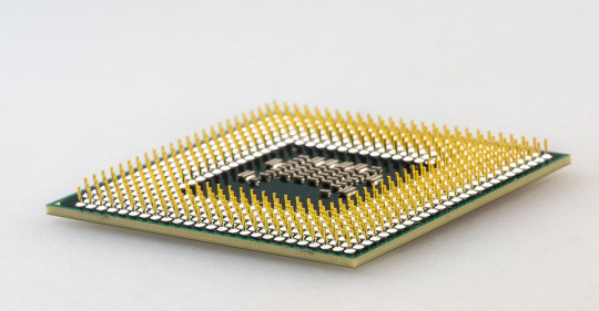
The Reports and Insights, a leading market research company, has recently releases report titled “Semiconductor Substrate Market: Global Industry Trends, Share, Size, Growth, Opportunity and Forecast 2025-2033.” The study provides a detailed analysis of the industry, including the global Semiconductor Substrate Market share, size, trends, and growth forecasts. The report also includes competitor and regional analysis and highlights the latest advancements in the market.
Report Highlights:
How big is the Semiconductor Substrate Market?
The global semiconductor substrate market was valued at US$ 13.9 Billion in 2024 and is expected to register a CAGR of 10.5% over the forecast period and reach US$ 34.1 Billion in 2033.
What are Semiconductor Substrate?
A semiconductor substrate is a fundamental material used as the base for manufacturing semiconductor devices, providing a stable platform for building electronic circuits and components. Typically composed of high-purity silicon, gallium arsenide, or other semiconductor materials, the substrate supports the deposition and patterning of layers that constitute the electronic devices. It is critical in determining the performance, reliability, and efficiency of the final semiconductor products, including integrated circuits and microchips. The selection and quality of the substrate material are vital for achieving the desired electrical characteristics and ensuring the proper functioning of the semiconductor device.
Request for a sample copy with detail analysis: https://www.reportsandinsights.com/sample-request/2390
What are the growth prospects and trends in the Semiconductor Substrate industry?
The semiconductor substrate market growth is driven by various factors and trends. The semiconductor substrate market is experiencing growth due to rising demand for sophisticated electronic devices, the expansion of technologies like 5G, and increased use in sectors such as automotive, consumer electronics, and industrial applications. Key factors driving this market include advancements in substrate materials like silicon, gallium arsenide, and silicon carbide, which improve the performance and efficiency of semiconductor devices. The market is also shaped by the need for greater precision and reliability in electronic components. Leading industry players are focusing on research and development to drive innovation in substrate technology. Although challenges such as fluctuating raw material prices and supply chain issues exist, the market is expanding thanks to ongoing technological advancements and the increasing complexity of semiconductor devices. Hence, all these factors contribute to semiconductor substrate market growth.
What is included in market segmentation?
The report has segmented the market into the following categories:
By Product Type
GaSb
InSb
GaN
Ga2O3
AlN
Diamond
Engineered
Others
By Application
Photonics
Electronics
By End User Industry
Automotive
Telecommunication
Consumer Electronics
Others
North America
United States
Canada
Europe
Germany
United Kingdom
France
Italy
Spain
Russia
Poland
Benelux
Nordic
Rest of Europe
Asia Pacific
China
Japan
India
South Korea
ASEAN
Australia & New Zealand
Rest of Asia Pacific
Latin America
Brazil
Mexico
Argentina
Middle East & Africa
Saudi Arabia
South Africa
United Arab Emirates
Israel
Rest of MEA
Who are the key players operating in the industry?
The report covers the major market players including:
Unimicron
LG Innotek
Samsung Electro-Mechanics
Nippon Mektron
AT&S
Korea Circuit
TTM Technologies
IBIDEN
Zhen Ding Tech
Compeg
Young Poong Group
View Full Report: https://www.reportsandinsights.com/report/Semiconductor Substrate-market
If you require any specific information that is not covered currently within the scope of the report, we will provide the same as a part of the customization.
About Us:
Reports and Insights consistently mееt international benchmarks in the market research industry and maintain a kееn focus on providing only the highest quality of reports and analysis outlooks across markets, industries, domains, sectors, and verticals. We have bееn catering to varying market nееds and do not compromise on quality and research efforts in our objective to deliver only the very best to our clients globally.
Our offerings include comprehensive market intelligence in the form of research reports, production cost reports, feasibility studies, and consulting services. Our team, which includes experienced researchers and analysts from various industries, is dedicated to providing high-quality data and insights to our clientele, ranging from small and medium businesses to Fortune 1000 corporations.
Contact Us:
Reports and Insights Business Research Pvt. Ltd. 1820 Avenue M, Brooklyn, NY, 11230, United States Contact No: +1-(347)-748-1518 Email: [email protected] Website: https://www.reportsandinsights.com/ Follow us on LinkedIn: https://www.linkedin.com/company/report-and-insights/ Follow us on twitter: https://twitter.com/ReportsandInsi1
#Semiconductor Substrate Market share#Semiconductor Substrate Market size#Semiconductor Substrate Market trends
0 notes
Text
Global LED Wafer and Chip Market: Key companies & Market Forecast to 2032
Global LED Wafer and Chip Market size was valued at US$ 18.76 billion in 2024 and is projected to reach US$ 28.45 billion by 2032, at a CAGR of 5.3% during the forecast period 2025-2032
LED Wafer and Chip Market Overview
The LED Wafer and Chip Market encompasses the manufacturing and commercialization of wafers and chips used in Light Emitting Diodes (LEDs). LED wafers serve as the substrate on which the LED is built, typically made from materials like sapphire, silicon carbide (SiC), or gallium nitride (GaN). These wafers are sliced into chips, which are then further processed and packaged for integration into lighting devices.
LED chips are the actual light-emitting components that are embedded in various lighting applications ranging from residential and commercial lighting to electronics, automotive headlights, and aerospace signaling systems. The wafer and chip form the core of the LED’s functionality, dictating brightness, efficiency, and longevity.
This market forms a critical part of the global semiconductor and optoelectronics industries, with strong interdependence on innovations in fabrication technology, substrate engineering, and miniaturization trends.
This report provides a deep insight into the global LED Wafer and Chip Market, covering all its essential aspects. This ranges from a macro-overview of the market to micro details of the market size, competitive landscape, development trend, niche market, key market drivers and challenges, SWOT analysis, value chain analysis, etc.
The analysis helps the reader to shape the competition within the industries and strategies for the competitive environment to enhance the potential profit. Furthermore, it provides a simple framework for evaluating and assessing the position of the business organization. The report structure also focuses on the competitive landscape of the Global LED Wafer and Chip Market. This report introduces in detail the market share, market performance, product situation, operation situation, etc., of the main players, which helps the readers in the industry to identify the main competitors and deeply understand the competition pattern of the market.
In a word, this report is a must-read for industry players, investors, researchers, consultants, business strategists, and all those who have any kind of stake or are planning to foray into the LED Wafer and Chip Market in any manner.
Get Full Report : https://semiconductorinsight.com/report/global-led-wafer-and-chip-market/
LED Wafer and Chip Key Market Trends :
Growing Demand for Energy-Efficient Lighting LED wafers and chips are increasingly adopted due to their energy-saving capabilities, replacing traditional lighting in homes, vehicles, and industries.
Miniaturization in Consumer Electronics Demand for compact and lightweight electronic devices is pushing the need for smaller, high-efficiency LED components.
Rising Automotive Applications Advanced LED lighting is becoming standard in modern vehicles, contributing significantly to market growth.
Increasing Investment in Smart Cities Smart street lighting and intelligent display systems are boosting LED wafer and chip installations.
Shift Towards GaN-Based LEDs Gallium Nitride-based LEDs are gaining traction for their higher efficiency and longer lifespan compared to traditional materials.
LED Wafer and Chip Market Regional Analysis :
North America:Strong demand driven by EVs, 5G infrastructure, and renewable energy, with the U.S. leading the market.
Europe:Growth fueled by automotive electrification, renewable energy, and strong regulatory support, with Germany as a key player.
Asia-Pacific:Dominates the market due to large-scale manufacturing in China and Japan, with growing demand from EVs, 5G, and semiconductors.
South America:Emerging market, driven by renewable energy and EV adoption, with Brazil leading growth.
Middle East & Africa:Gradual growth, mainly due to investments in renewable energy and EV infrastructure, with Saudi Arabia and UAE as key contributors.
LED Wafer and Chip Market Segmentation :
The research report includes specific segments by region (country), manufacturers, Type, and Application. Market segmentation creates subsets of a market based on product type, end-user or application, Geographic, and other factors. By understanding the market segments, the decision-maker can leverage this targeting in the product, sales, and marketing strategies. Market segments can power your product development cycles by informing how you create product offerings for different segments.
Market Segmentation (by Application)
Electronic Products
Car
Space
Other
Market Segmentation (by Type)
LED Wafer
LED Chip
Key Company
Nichia
SAMSUNG
EPISTAR
Cree
Osram
PHILIPS Lumileds
SSC
LG Innotek
Toyoda Gosei
Semileds
Hewlett Packard
Lumination
Bridgelux
Drivers
Growing Demand for Energy-Efficient Products Rising energy costs and government initiatives to reduce carbon footprints are driving the demand for LED-based lighting systems.
Expansion of Automotive and Consumer Electronics Sectors Wider use of LEDs in automotive lighting, smartphones, TVs, and wearables is fueling market growth.
Advancement in LED Technology Ongoing innovations in chip architecture and wafer materials are enhancing performance, reducing heat, and increasing durability.
Restraints
High Initial Investment Costs Despite long-term savings, the upfront cost of LED wafer and chip manufacturing can deter small-scale producers.
Supply Chain Disruptions Geopolitical tensions and reliance on specific regions for raw materials can impact the production cycle and availability.
Technical Limitations in Heat Dissipation LED chips can face efficiency drops due to thermal management challenges, especially in high-power applications.
Opportunities
Adoption in Smart Lighting and IoT Devices LED integration in smart homes and IoT-connected devices presents new revenue avenues for manufacturers.
Rising Demand in Emerging Economies Developing countries are adopting LED lighting at a fast pace due to energy-saving initiatives and infrastructure upgrades.
Use in Aerospace and Industrial Applications Specialized applications in aerospace, healthcare, and industrial sectors are opening up high-margin segments.
Challenges
Intense Competition and Price Pressure Presence of numerous global and regional players leads to aggressive pricing, impacting profit margins.
Rapid Technological Changes Constant advancements require companies to invest heavily in R&D to stay competitive.
Environmental Concerns Related to E-Waste Improper disposal of LED chips and wafers may contribute to electronic waste, raising sustainability concerns.
Get A Sample Report : https://semiconductorinsight.com/download-sample-report/?product_id=96487
Key Benefits of This Market Research:
Industry drivers, restraints, and opportunities covered in the study
Neutral perspective on the market performance
Recent industry trends and developments
Competitive landscape & strategies of key players
Potential & niche segments and regions exhibiting promising growth covered
Historical, current, and projected market size, in terms of value
In-depth analysis of the Flash Memary Market
Overview of the regional outlook of the Flash Memary Market:
Key Reasons to Buy this Report:
Access to date statistics compiled by our researchers. These provide you with historical and forecast data, which is analyzed to tell you why your market is set to change
This enables you to anticipate market changes to remain ahead of your competitors
You will be able to copy data from the Excel spreadsheet straight into your marketing plans, business presentations, or other strategic documents
The concise analysis, clear graph, and table format will enable you to pinpoint the information you require quickly
Provision of market value (USD Billion) data for each segment and sub-segment
Indicates the region and segment that is expected to witness the fastest growth as well as to dominate the market
Analysis by geography highlighting the consumption of the product/service in the region as well as indicating the factors that are affecting the market within each region
Provides insight into the market through Value Chain
Market dynamics scenario, along with growth opportunities of the market in the years to come
6-month post-sales analyst support
Customization of the Report In case of any queries or customization requirements, please connect with our sales team, who will ensure that your requirements are met.
Related Reports :
Contact us:
0 notes
Text
3D IC Market Size, Share, Trends, Key Drivers, Demand and Opportunity Analysis
3D IC Market Segmentation, By Component (LED, Memories, MEMS, Sensor, Logic and Others), Application (Logic, Imaging and Optoelectronics, Memory, MEMS/Sensors, LED, Power, Analog and Mixed Signal, RF, Photonics and Others), Substrate (Silicon on Insulator and Bulk Silicon), Technology (3D Wafer-Level Chip-Scale Packaging (WLCSP), 3D TSV, Silicon Epitaxial Growth, Beam Re-Crystallization, Solid Phase Crystallization and Wafer Bonding), End-User Industry (Consumer Electronics, Telecommunication, Industrial Sector, Automotive, Military and Aerospace, Smart Technologies, and Medical Devices) – Industry Trends and Forecast to 2032
The global 3d IC market size was valued at USD 9.47 billion in 2024 and is projected to reach USD 92.72 billion by 2032, with a CAGR of 33.00% during the forecast period of 2025 to 2032.
The 3D IC Market report is the best to know the trends and opportunities in industry. The forecast, analysis, evaluations and estimations carried out in this 3D IC Market report are all based upon the well established tools and techniques such as SWOT analysis and Porter’s Five Forces analysis. These are the authentic tools used in market analysis on which businesses can trust confidently. This 3D IC Market report brings into focus plentiful of factors such as the general market conditions, trends, inclinations, key players, opportunities, and geographical analysis which all aids to take your business towards the growth and success.
This 3D IC Market report also estimates the growth rate and the market value based on market dynamics and growth inducing factors. It is a well-versed fact that competitive analysis is the major aspect of any market research report and hence many points are covered under this including strategic profiling of key players in the market, analyse core competencies of key players, and draw a competitive landscape for the market. This global 3D IC Market business report has been built with the careful efforts of innovative, enthusiastic, knowledgeable and experienced team of analysts, researchers, industry experts, and forecasters.
Discover the latest trends, growth opportunities, and strategic insights in our comprehensive 3D IC Market report. Download Full Report: https://www.databridgemarketresearch.com/reports/global-3d-ic-market
3D IC Market Overview
**Segments**
- **By Technology**: Through-Silicon Via (TSV), Silicon Interposer, 3D IC Packaging. - **By End-User**: Consumer Electronics, Telecommunication, Industrial, Automotive, Military & Aerospace, Healthcare, Others. - **By Application**: Logic, Imaging & Optoelectronics, Memory, MEMS/sensors, LED.
The global 3D IC market is segmented based on technology, end-user, and application. The technology segment includes Through-Silicon Via (TSV), Silicon Interposer, and 3D IC Packaging. TSV technology has gained significant traction in recent years as it allows for vertical integration of multiple dies, leading to enhanced performance and miniaturization. The Silicon Interposer segment is also witnessing growth due to its ability to facilitate high-bandwidth communication between stacked dies. In terms of end-users, the market caters to various industries such as consumer electronics, telecommunication, automotive, healthcare, and more. Each sector has unique requirements for 3D ICs, driving the demand for customized solutions. Additionally, the application segment includes logic, imaging & optoelectronics, memory, MEMS/sensors, and LED, each playing a crucial role in different electronic devices.
**Market Players**
- **Samsung Electronics Co., Ltd.**: A key player in the global 3D IC market, Samsung offers a wide range of 3D IC solutions catering to diverse end-user industries. - **Taiwan Semiconductor Manufacturing Company Limited**: TSMC is known for its advanced semiconductor technologies and plays a significant role in the development of 3D ICs. - **Advanced Semiconductor Engineering, Inc.**: ASE provides innovative packaging solutions, including 3D IC technology, to meet the evolving demands of the market. - **Xilinx, Inc.**: Xilinx specializes in programmable devices and 3D IC technologies, offering high-performance solutions to its customers. - **Tezzaron Semiconductor Corporation**: Known for its pioneering work in 3D IC technology, Tezzaron continues to push the boundaries of semiconductor innovation.
These market players are at the forefront of driving innovation and growth in the global 3D IC market. By investing in research and development, forging strategic partnerships, and expanding their product portfolios, these companies are shaping the future of 3D IC technology.
The global 3D IC market is poised for significant growth in the coming years, driven by advancements in technology, increasing demand for high-performance electronic devices, and the expanding applications across various industries. One key trend that is expected to shape the market is the rising adoption of 3D IC packaging solutions in the consumer electronics sector. With consumers demanding more powerful and energy-efficient devices, manufacturers are turning to 3D IC technology to meet these requirements. This trend is further fueled by the growing popularity of smartphones, tablets, wearables, and other personal electronic devices that rely on compact, high-performance semiconductor solutions.
Moreover, the telecommunication industry is also a major contributor to the growth of the 3D IC market. With the deployment of 5G networks and the increasing demand for faster and more reliable communication systems, telecom companies are looking for advanced semiconductor solutions that can enhance network performance and efficiency. 3D IC technology, with its ability to increase device density and reduce power consumption, is well-suited to address these challenges and drive innovation in the telecommunication sector.
In the automotive industry, the demand for advanced driver-assistance systems (ADAS), autonomous vehicles, and in-vehicle infotainment systems is creating opportunities for 3D IC integration. By incorporating 3D IC technology into automotive electronics, manufacturers can achieve higher levels of performance, reliability, and efficiency, ultimately enhancing the driving experience and safety features of modern vehicles.
Additionally, the healthcare sector is also leveraging 3D IC technology to develop innovative medical devices, diagnostic equipment, and implantable devices. The ability of 3D ICs to enable miniaturization, increase functionality, and improve signal processing capabilities is driving their adoption in healthcare applications, leading to improved patient care and medical advancements.
Overall, the global 3D IC market is characterized by intense competition, rapid technological advancements, and evolving end-user requirements. Market players need to focus on R&D efforts, innovation, and strategic collaborations to stay ahead in this dynamic landscape. As the demand for high-performance, energy-efficient semiconductor solutions continues to rise across different industries, the 3D IC market is expected to witness sustained growth and offer lucrative opportunities for both established players and new entrants.The global 3D IC market is experiencing significant growth and transformation across various segments. One key driver of this growth is the increasing demand for high-performance electronic devices in industries such as consumer electronics, telecommunication, automotive, healthcare, and more. The adoption of 3D IC technology is on the rise as it offers advanes such as enhanced performance, miniaturization, and improved energy efficiency. This trend is particularly prominent in the consumer electronics sector, where manufacturers are under pressure to deliver more powerful and compact devices to meet consumer demands.
In the telecommunication industry, the deployment of 5G networks and the need for faster communication systems are driving the adoption of 3D IC solutions to enhance network performance and efficiency. Additionally, in the automotive sector, the demand for advanced driver-assistance systems and autonomous vehicles is creating opportunities for 3D IC integration to achieve higher levels of performance and reliability.
The healthcare industry is also leveraging 3D IC technology for the development of innovative medical devices and diagnostic equipment. The miniaturization and increased functionality enabled by 3D ICs are enhancing patient care and driving advancements in medical technology.
Key market players such as Samsung Electronics, TSMC, ASE, Xilinx, and Tezzaron are leading the way in driving innovation and growth in the 3D IC market. These companies are investing in R&D, forming strategic partnerships, and expanding their product portfolios to stay competitive in the dynamic market landscape.
Overall, the global 3D IC market is characterized by intense competition, rapid technological advancements, and evolving end-user requirements. Market players need to focus on innovation, collaboration, and continuous improvement to capitalize on the growing demand for high-performance semiconductor solutions across various industries. With the market poised for significant growth in the coming years, there are lucrative opportunities for both established players and new entrants to capture a share of this expanding market.
The 3D IC Market is highly fragmented, featuring intense competition among both global and regional players striving for market share. To explore how global trends are shaping the future of the top 10 companies in the keyword market.
Learn More Now: https://www.databridgemarketresearch.com/reports/global-3d-ic-market/companies
DBMR Nucleus: Powering Insights, Strategy & Growth
DBMR Nucleus is a dynamic, AI-powered business intelligence platform designed to revolutionize the way organizations access and interpret market data. Developed by Data Bridge Market Research, Nucleus integrates cutting-edge analytics with intuitive dashboards to deliver real-time insights across industries. From tracking market trends and competitive landscapes to uncovering growth opportunities, the platform enables strategic decision-making backed by data-driven evidence. Whether you're a startup or an enterprise, DBMR Nucleus equips you with the tools to stay ahead of the curve and fuel long-term success.
Key Questions Answered in This Report: –
How has this 3D IC Marketperformed so far and how will it perform in the coming years?
Which are the key product types available in this 3D IC Market?
Which are the major application areas in the3D IC Market?
What are the key distribution channels in the global 3D IC Market?
What are the key regions in this 3D IC Market?
What are the price trends?
What are the various ses in the value chain of this industry?
What are the key driving factors and challenges in the market?
Browse More Reports:
Europe Fuel Cards for Commercial Fleet Market Global Millimeter Wave Radar Vision System Market Global CNG Tanks Cylinders Market Global Antistatic Electrostatic Discharge (ESD) Foam Market Global Usage-Based Insurance for Automotive Market Global Viral Clearance Services Market Global 3D Food Printing Market Global Food Diagnostics Market Asia-Pacific Cervical Cancer Diagnostic Market Global Telestroke Market Global Anti-Dermatomycosis Skin Drugs Market Global Heparin Market Global Packaging Pumps and Dispensers Market Global Avocado Oil Market Global Transparent Caching Market Global Toaster Oven Market Global Paperboard Jar Market Global P2X7 Receptor Anonists Market Global CT Scanner Market Global enterprise content management (ECM) services Market Asia-Pacific Heparin Market Global Industrial Centrifuge Market Europe Massive Open Online Courses (MOOCs) Market Global Leak Detection Market Global Kearns-Sayre Syndrome Market Europe and Middle East Heparin Market Global Phosphodiesterase (PDE) Inhibitors Market Global Defoaming Coating Additives Market Global Oats Market Global Bentonite Market Global Klebsiella Infection Market Global Agent Performance Optimization (APO) Market Europe Busbar in EVSE Market North America Whole Exome Sequencing Market Europe Polyglycolic Acid Market in Oil and Gas industry - Industry Trends and Forecast to 2029 Global Digital Process Automation Market
About Data Bridge Market Research:
An absolute way to forecast what the future holds is to comprehend the trend today!
Data Bridge Market Research set forth itself as an unconventional and neoteric market research and consulting firm with an unparalleled level of resilience and integrated approaches. We are determined to unearth the best market opportunities and foster efficient information for your business to thrive in the market. Data Bridge endeavors to provide appropriate solutions to the complex business challenges and initiates an effortless decision-making process. Data Bridge is an aftermath of sheer wisdom and experience which was formulated and framed in the year 2015 in Pune.
Contact Us: Data Bridge Market Research US: +1 614 591 3140 UK: +44 845 154 9652 APAC : +653 1251 975 Email:- [email protected]
0 notes
Text
Die Bonder Equipment Market to See Gradual Rise, Surpassing $2.8 Billion by 2034

Market Overview
The Die Bonder Equipment Market plays a critical role in the semiconductor packaging and assembly industry. This market centers around machines that mount semiconductor dies onto packages, substrates, or wafers with high precision and reliability. The surging demand for smaller, more efficient electronic devices has led to a growing requirement for advanced packaging solutions—consequently pushing the need for die bonding technology. As the global semiconductor industry rapidly evolves, die bonder equipment has become a foundational component in supporting processes such as flip-chip bonding, wire bonding, and eutectic bonding.
Die bonder equipment comes in various forms, including fully automatic, semi-automatic, and manual machines. With the rise in automation and demand for high-volume manufacturing, fully automatic die bonders are gaining significant traction. This is especially relevant in applications ranging from consumer electronics and telecommunications to industrial systems and automotive electronics.
Click to Request a Sample of this Report for Additional Market Insights: https://www.globalinsightservices.com/request-sample/?id=GIS22629
Market Dynamics
Several dynamic factors are shaping the Die Bonder Equipment Market. Firstly, the increasing adoption of miniaturized electronic components in smartphones, wearables, and medical devices is fueling demand for high-speed, high-precision bonding equipment. Hybrid and multi-function bonder types are also witnessing a boost due to their compatibility with different bonding technologies such as epoxy, eutectic, and soft solder die bonding.
Moreover, the rise of electric vehicles (EVs) and advancements in automotive electronics are accelerating market growth. EVs demand robust, temperature-resistant semiconductor components, which in turn require efficient bonding technologies. The demand for die bonders with improved functionality, such as better vision systems and bonding heads, is growing accordingly.
However, challenges like the high initial cost of fully automatic die bonders and the technical complexity of hybrid bonding methods could hamper widespread adoption among small- and mid-sized enterprises. Still, with the advancement in Industry 4.0 and the integration of AI and IoT into bonding machines, manufacturers are overcoming traditional limitations.
Key Players Analysis
The Die Bonder Equipment Market features several key players who are constantly innovating to stay ahead in the competitive landscape. Major players include ASM Pacific Technology, Kulicke & Soffa, Palomar Technologies, SHINKAWA Ltd., and BESI (BE Semiconductor Industries). These companies are investing heavily in R&D to improve bonding speed, precision, and system versatility.
For instance, companies like Kulicke & Soffa are leading the development of flip-chip and hybrid die bonding machines with advanced vision alignment systems, while Palomar Technologies is known for offering high-speed die attach systems suited for optoelectronic and power semiconductor packaging. Collaborations and strategic mergers are also becoming increasingly common as players seek to expand their technological portfolios and geographical presence.
Regional Analysis
Geographically, Asia-Pacific dominates the die bonder equipment market due to the strong presence of semiconductor manufacturing hubs in countries like China, Taiwan, South Korea, and Japan. The region benefits from massive investments in electronics manufacturing, favorable government policies, and robust supply chains.
North America holds a significant share as well, led by the U.S., where innovation in consumer electronics and defense applications is prominent. Europe, particularly Germany and the Netherlands, is making strides in precision engineering and automation, which supports die bonding system advancements.
Emerging markets in Latin America and the Middle East & Africa are expected to grow at a steady pace, driven by increasing investment in telecom infrastructure and electronics assembly.
Recent News & Developments
The Die Bonder Equipment Market has recently seen a wave of technological upgrades. Companies are rolling out machines with machine-learning capabilities and predictive maintenance systems. For example, ASM Pacific has introduced AI-powered die bonders that optimize bonding processes in real time. There has also been a notable increase in the adoption of retrofit installations, allowing older equipment to be upgraded with modern features, offering cost-effective solutions to manufacturers.
Another important development is the integration of hybrid die bonding technology, which combines the advantages of multiple bonding techniques to deliver both speed and reliability. This innovation is gaining traction in the healthcare device sector, where microelectronic performance is critical.
Browse Full Report @ https://www.globalinsightservices.com/reports/die-bonder-equipment-market/
Scope of the Report
The Die Bonder Equipment Market is poised for considerable growth, driven by the expanding semiconductor and electronics manufacturing industries. The report provides a comprehensive analysis of market segmentation based on type (fully automatic, semi-automatic, manual), product (flip chip bonder, wire bonder, die attach equipment), technology (epoxy, eutectic, soft solder, hybrid), and applications (consumer electronics, automotive, healthcare, telecommunications, industrial).
Moreover, it explores in-depth the impact of installation types—new vs. retrofit—and evaluates market trends shaped by AI integration, high-precision needs, and multi-functionality in modern equipment. With innovation and automation reshaping the die bonding landscape, the future outlook for this market remains highly promising.
Discover Additional Market Insights from Global Insight Services:
Septic Solutions Market: https://www.globalinsightservices.com/reports/septic-solutions-market/
Artillery Ammunition Market: https://www.globalinsightservices.com/reports/artillery-ammunition-market/
Concrete Pump Market: https://www.globalinsightservices.com/reports/concrete-pump-market/
Spring Energized Seals Market: https://www.globalinsightservices.com/reports/spring-energized-seals-market/
Die Bonder Equipment Market: https://www.globalinsightservices.com/reports/die-bonder-equipment-market/
0 notes
Text
Diamond Substrate Industry Insights Opportunities, Key Applications & Market Dynamics
The global Diamond Substrate Market is gaining significant momentum due to increasing demand for high-performance materials across the semiconductor, electronics, and photonics industries. With a market value projected to reach over USD 265 million by 2030, the sector is expected to grow at a steady CAGR of around 6 %. Key growth factors include superior thermal conductivity, high breakdown voltage, and compatibility with next-generation devices such as quantum computers, RF amplifiers, and power electronics. Diamond substrates engineered using advanced chemical vapor deposition (CVD) techniques—are becoming essential components in applications that demand exceptional thermal and electrical performance. These substrates are gaining ground in high-frequency, high-power, and high-precision devices, making them an indispensable element in future electronics.
The market is driven by the shift towards advanced semiconductor technologies, especially in the telecommunications, automotive, aerospace, and defense industries. Synthetic diamond substrates, particularly those created using microwave plasma-assisted CVD, offer high purity and consistent quality, making them ideal for emerging use cases such as GaN-on-diamond technology and quantum photonic chips.
North America leads the global landscape due to early adoption in defense and aerospace sectors, while Asia-Pacific, particularly Japan and South Korea, is rapidly scaling production capacities and driving demand for diamond-based power devices.
The industry is also witnessing significant R&D investments in developing large-diameter diamond wafers, a crucial development to meet rising demands in industrial, electronic, and thermal management applications.
Market Segmentation
By Type
Electronic-grade diamond substrates: Used in semiconductors and photonic devices.
Mechanical-grade substrates: Suitable for industrial tools and coatings.
Optical-grade substrates: Utilized in laser systems and high-precision optics.
By Form Factor
Wafers: Widely used in high-power and RF electronics.
Films and coatings: Applied in medical, cutting, and industrial tooling segments.
By Technology
Chemical Vapor Deposition (CVD): Hot filament and microwave plasma methods dominate due to quality control and scalability.
High Pressure High Temperature (HPHT): Less common but still used in certain industrial-grade applications.
By Application
Semiconductors & Electronics
Telecommunication Devices
Medical and Biotechnology Tools
Thermal Management Systems
Industrial Cutting and Wear Tools
By End-Use Industry
Electronics and Semiconductor
Medical and Biotechnology
Aerospace and Defense
Industrial Manufacturing
By Region
North America
Europe
Asia-Pacific
Middle East & Africa
Latin America
Key Market Trends
Rising Semiconductor Integration The push for more efficient and compact semiconductor designs, especially in power devices and RF communication, is propelling demand for diamond substrates due to their superior thermal and dielectric performance.
Growth in Quantum Computing Diamond’s nitrogen-vacancy (NV) centers make it a foundational material in quantum sensors and communication systems, opening new commercial avenues.
Advancements in Deposition Technology Innovations in CVD techniques are enabling large-area, defect-free substrates, making production more cost-effective and scalable.
Thermal Management Solutions The need for efficient heat dissipation in compact electronics is driving interest in diamond substrates, especially in laser systems and 5G equipment.
North America’s Technological Edge Leading companies and research institutes in the U.S. and Canada are pioneering diamond-based integration in aerospace, defense, and high-frequency devices.
Segment Insights
Electronics and Semiconductor
This segment commands the largest share due to the increasing use of diamond substrates in RF power devices, GaN HEMTs, and high-voltage switching applications. These substrates enhance device performance and longevity by addressing thermal and voltage breakdown challenges.
Medical and Biotechnology
Diamond coatings are favored for surgical tools and implantable devices due to their biocompatibility and resistance to microbial growth. The growing healthcare infrastructure worldwide is expected to fuel further adoption.
Industrial Manufacturing
Mechanical-grade diamond substrates are widely used in cutting, drilling, and wear-resistant applications, especially in mining, automotive, and heavy engineering.
Aerospace and Defense
Diamond substrates enable enhanced performance in radar systems, laser targeting, and secure quantum communication, aligning with growing defense modernization efforts.
End-User Insights
Semiconductor Manufacturers
Companies focusing on high-frequency and power electronics are the largest consumers of diamond substrates. Integration with GaN and SiC technologies is accelerating.
Defense Contractors
High-reliability radar and quantum sensing devices increasingly rely on diamond for durability and performance in extreme conditions.
Medical Device OEMs
Manufacturers are investing in diamond-coated surgical and diagnostic equipment, especially for applications where precision and hygiene are critical.
Tooling and Industrial Equipment Firms
Diamond’s extreme hardness and wear resistance make it ideal for cutting tools, surface coatings, and heat-resistant components.
Key Players
Prominent companies in the diamond substrate market are emphasizing R&D, strategic partnerships, and vertical integration to enhance their capabilities and market presence. Some of the leading players include:
Sumitomo Electric Industries, Ltd. – Focused on high-purity diamond materials for electronics and photonics.
Element Six (De Beers Group) – A global leader in synthetic diamond technologies and CVD wafer production.
Advanced Diamond Technologies – Specializes in thin diamond films for semiconductor and thermal management applications.
IIa Technologies – One of the largest CVD diamond manufacturers for industrial and electronics use.
Applied Diamond Inc. – Supplies single-crystal and polycrystalline substrates for R&D and commercial markets.
Trending Report Highlights
Microcontroller Unit Market
Digital Mobile Radio Market
Embedded Systems Market
USB Devices Market
Quantum Dots Market
0 notes
Text
Europe Semiconductor Bonding Market Size, Revenue, End Users And Forecast Till 2028
The semiconductor bonding market in Europe is expected to grow from US$ 215.77 million in 2022 to US$ 349.17 million by 2028. It is estimated to grow at a CAGR of 8.4% from 2022 to 2028.
Market Overview
Germany, France, Italy, Russia, the UK, and rest of Europe are the key contributors to the semiconductor bonding market in the Europe. A stacked die is an assembly technique where two or more die is stacked and bonded in a single semiconductor package. It is used on a substrate having numerous functionalities around the same placement area. The performance of electrical devices is enhanced due to die piling. Thus, the utilization of stacked die is one of the major drivers accelerating the market growth. EV Group, HUTEM are a few of the prominent companies operating in the Europe semiconductor bonding market. These companies are majorly focusing on the market for MEMS sensors, CMOS image sensors, and RF devices. For instance, in March 2022, Merck KGaA, a Germany-based pharmaceutical company, announced a total investment of US$ 82 million to build a new semiconductor facility in Zhangjiagang, China. The growth of wafer bonding is fueled by the growing demand for various thermal imaging applications, including night vision systems for military and security use, imaging systems to improve building construction, thermal cameras for pedestrian protection systems in automobiles, and process monitoring systems for several commercial and industrial applications.
Grab PDF To Know More @ https://www.businessmarketinsights.com/sample/BMIRE00027611
Europe Semiconductor Bonding Strategic Insights
Strategic insights for the Europe Semiconductor Bonding provides data-driven analysis of the industry landscape, including current trends, key players, and regional nuances. These insights offer actionable recommendations, enabling readers to differentiate themselves from competitors by identifying untapped segments or developing unique value propositions. Leveraging data analytics, these insights help industry players anticipate the market shifts, whether investors, manufacturers, or other stakeholders. A future-oriented perspective is essential, helping stakeholders anticipate market shifts and position themselves for long-term success in this dynamic region. Ultimately, effective strategic insights empower readers to make informed decisions that drive profitability and achieve their business objectives within the market.
Market leaders and key company profiles
ASMPT
DIAS Automation (HK) Ltd.
EV Group
HUTEM
Kulicke & Soffa Industries, Inc.
Palomar Technologies
Panasonic Corporation
Toray Industries Inc
WestBond, Inc.
Yamaha Motor Corporation
Europe Semiconductor Bonding Regional Insights
The geographic scope of the Europe Semiconductor Bonding refers to the specific areas in which a business operates and competes. Understanding local distinctions, such as diverse consumer preferences (e.g., demand for specific plug types or battery backup durations), varying economic conditions, and regulatory environments, is crucial for tailoring strategies to specific markets. Businesses can expand their reach by identifying underserved areas or adapting their offerings to meet local demands. A clear market focus allows for more effective resource allocation, targeted marketing campaigns, and better positioning against local competitors, ultimately driving growth in those targeted areas.
Europe Semiconductor Bonding Market Segmentation
The Europe semiconductor bonding market is segmented into type, application, and country.
Based on type, the market is segmented into die bonder, wafer bonder, and flip chip bonder. The wafer bonder segment registered the largest market share in 2022.
Based on application, the market is segmented into RF devices, MEMS and sensors, LED, CMOS image sensors, and 3D NAND. The MEMS and sensors segment held a largest market share in 2022.
Based on country, the market is segmented into Germany, France, Italy, Russia, the UK, and rest of Europe. Germany dominated the market share in 2022.
About Us:
Business Market Insights is a market research platform that provides subscription service for industry and company reports. Our research team has extensive professional expertise in domains such as Electronics & Semiconductor; Aerospace & Defence; Automotive & Transportation; Energy & Power; Healthcare; Manufacturing & Construction; Food & Beverages; Chemicals & Materials; and Technology, Media, & Telecommunications.
0 notes