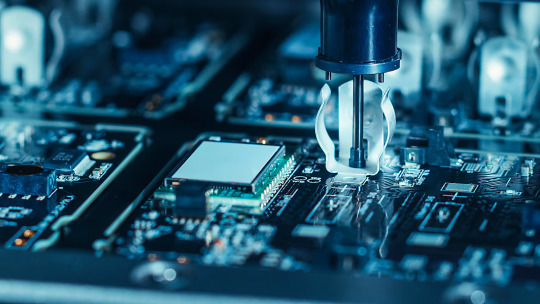
#Surface Mount Technology (SMT) assembly
Explore tagged Tumblr posts
Visit Tumblr Blog
Explore Tumblr blogs with no restrictions, modern design and the best experience.
Last Seen Tumblr Blogs


Fun Fact
Tumblr has been providing a Korean-language service since 2013.
Text
Discover the basics of SMT assembly in this introductory guide. Learn about Surface Mount Technology (SMT), its components, assembly process, and its significance in electronics manufacturing.
0 notes
Text
Selective soldering 🔧🔬🔥
Selective soldering involves attaching specific components to printed circuit boards (PCBs) and molded modules, a method particularly useful for items susceptible to heat damage from standard reflow ovens or wave soldering found in conventional surface-mount technology (SMT) or through-hole assembly techniques. Typically, this method is applied after an initial SMT oven reflow phase. The components targeted for selective soldering are often nestled among others already soldered via a surface-mount reflow method. This demands high precision in the selective soldering process to prevent damage to the surrounding elements.
#adafruit#selectivesoldering#pcbassembly#electronicsmanufacturing#surface-mount#throughhole#reflowprocess#precisionengineering#solderingtechnology#circuitboarddesign#manufacturinginnovation#techadvancements
5 notes
·
View notes
Text
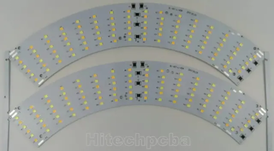
LED PCB Assembly
What is the LED Circuit Board assembly?
Generally, LED PCB assembly is considered to be a circuit board that has the LED components soldered to it. The LED is soldered to the printed circuit board and features a chip that creates the light as electrically connected. A thermal heat sink and a ceramic base are used to bond the chip. Not all the PCB products can be used in Led industry, as an LED PCB is easy to create a high volume of heat, but making it hard to cool with traditional methods. For this reason, metal core PCB is widely used in LED application because of their enhanced ability to dissipate heat, especially aluminum pcb is often used to fabricate PCB for LED lights.
We’ve had great LED PCB assembly experiences with top LED chips to brand such as Cree, Luxeon, Osram, Nichia, Lumileds, MLS, EVERLIGHT, Samsung, LG, Seoul., etc. PCB LED lights can be incorporated into numerous lighting applications due to their combination of excellent energy efficiency, low cost and maximum design flexibility.

Application of LED PCB Assembly
Hitechpcba serves customers in different industries, providing highly reliable and innovative LED PCBs for various applications:
• Horticulture light LED PCB Assembly
• LED controller PCB Assembly
• Computer LED display and indicators
• LED lights PCB Assembly for medical use
• Automotive LED PCBs Assembly include PCBs for brake lights and headlights
• Street lighting LED PCB Assembly
• Flashlights and camping accessories
• Traffic light PCB Assembly
• Commercial lighting LED PCB Assembly
LED PCB Assembly specification
Number of layers for LED PCB
These layers are made up of aluminum and magnesium, but now have Copper base material and Ceramic base materials for LED PCB industry, we can meet it.
Aluminum LED PCBs stand out among other PCBs because it has a good insulation characteristic and has a better machinery performance, the cheap cost is one important factor too.
Types of layers for LED PCB Assembly
Normally, the base layer is made using aluminum alloy metal.
This aluminum alloy substrate used in making the base makes it ideal for through-hole technology which transfers and dissipates heat.
A thermal insulation layer is made using some ceramic polymer which has good viscoelasticity characteristics.
It is highly heat resistant and protects the PCB against heat and mechanical stress.
The circuit layer, which is covered by a copper foil which can range from one to ten ounces.
LED Board type- single or in panel
Some boards are shapeless. For this reason, LED PCB panels are used. This reduces time, labor production and testing time.
Some LED PCB Assembly is done on a single board while others are done on panel boards.
LED PCB Assembly Process
Roughly, the PCBA process can be divided into theses phases: soldering paste printing > SMT (surface mounted technology) > reflow soldering > AOI (automated optical inspection)> THT (through-hole technology) > wave soldering > touch-up and cleaning > IC-programming > FCT (functional tests) > aging testing.
Below we show you the process.
Step1. Summarizing Project Information
Before contacting your supplier, make sure you have all the project information. Suppliers will need info following for quoting LED PCB assembly:
Gerber
BOM
LED PCB specification
Quotation quantity
Once you have gathered these information, you can contact us and request for a quote.
Of course, you can also provide the schematic, LED PCB Assembly pictures and even samples to us. The more details they have, the more accurate the supplier’s quotation will be.
Step2. Discussion and details about custom LED PCB Assembly
Different projects will have different requirements. Remember the special requirements mentioned in step 1? That’s going to be the focus of this session. Equipment and engineering capacity will not be identical between suppliers. Make sure your supplier has the equipment to produce and assemble major components and the corresponding testing capabilities.
For example, some vendors don’t have X-ray testing equipment, which means they can’t check the mount quality of BGA chips. Outsourcing this step will increase risk and cost. That’s what you don’t want.
Also, pay attention to time taken by the supplier to quote. Motherboards often contain hundreds or even thousands of components, and they are supplied by different manufacturers. To ensure the quality of the components, the supplier sourcing team will make multi-inquiries from these manufacturers or authorized suppliers to match customer’s requirement, which usually takes 2-3 business days, and even longer for some scarce chips. Therefore, if your project is complex and the supplier quotes you within few hours, double check with them.
Step3. Sample and feedback
After confirming the PI, the supplier will usually provide pre-production samples for your approval. At the same time, the supplier will also confirm with you the logistics plan of the bulk goods. Make sure they understand your shipping requirements, including details on packaging, customs clearance, taxes, etc.
For us to have a successful LED PCB Assembly process, its functions must be defined. Compliance requirement is defined to reduce the effect when components are selected.
The Bill of Materials is then generated from the information installed on the LED PCB.
All this information is used to assemble components which are identified from MOB to the LED PCB.
After that, the routing of traces is determined to each component, based on the size, shape of the circuit board and location of connectors.

Hitech Circuits is trusted by thousands of electronic engineers on their LED PCB assembly projects, from consumer, led bulb to precisely medical LED light, we can help you from the beginning of design stage; From commercial flood LED to industrial high power LED, from automotive LED to military LED, Venture is the perfect place for your LED PCB assembly requirement.
Hitech Circuits has been participated in hundreds and thousands of LED lighting projects, by providing LED PCB and also LED PCB assembly service.
Our LED PCB assembly had covered both ends of the Lighting Class LED size spectrum, assembling some of the largest (2 meter long boards) and some of the smallest LED Lighting applications which used in Medical Endoscopes.
LED PCB Assembly is very crucial in the current industrial development. Many electrical devises are being innovated and the old once being improved.
LED PCBs are useful due to the fact that they are made using materials that can transfer and dissipate heat. This characteristic increases device durability.
The world is changing with new technology, especially PCB technology that plays an essential role in the application of LED circuits. And the LED industry is taking advantage of this technology and growing faster.
As a full feature PCB solutions provider with more than a decade of experience, we're capable to provide LED PCB fabrication, components procurement and LED PCB assembly all under one roof. We can work with you to develop metal core PCB, aluminum circuit boards customized to your specific applications. We feature competitively priced PCBs made with standard FR-4 material that includes a thermal aluminum clad layer that will efficiently dissipate heat, keep all LED PCB components cool and significantly enhance the performance of your products.

LED pcb board, LED pcb assembly
LED with its advantages of high brightness, high efficiency, low heat, long life, is considered the most development potential in the 21st century lighting. In the market and policy driven by the rapid development of the domestic LED industry blowout has formed a relatively complete industrial chain, including the production of epitaxial wafers, chip preparation, packaging, integration, LED application. In 2010, China's LED industry scale, up from $ 827 billion in 2019 to 220 billion yuan, an annual growth rate of over 70%, higher than the 50% level of growth of the global LED lighting industry output value. Among them, the middle and lower reaches of the most complete industrial chain, accounting for 90% of the overall percentage of the GDP.Chinahas become the world's leading LED manufacturing base and important application market.
To further promote the technological innovation of the LED industry, construction and wide application of independent industry chain, China Electronic Appliance Corporation and industry associations to organize the theme of "Focus on the core energy LED Exhibition will be held November 9-11, 2010 in Shanghai International Expo Center and the 78th China Electronics Fair over the same period will be held will create from raw materials, epitaxial wafers, chip, LED bracket, LED accessories, LED packaging and supporting materials, the LED backlight upstream firm to the upstream and downstream enterprises of the display, lighting, landscaping, decorative lighting, traffic lights, automotive lighting, special lighting, to the equipment, instrumentation, software, finance, consulting and other service enterprises and technological exchanges and market trading platform, help the domestic industry sustained and healthy development, and promote the steady expansion of the LED application market.
In the LED industry chain upstream of the epitaxial wafers and LED chips accounted for 70% of the profits of the whole industry, and technology-intensive, capital-intensive, where the core technology of the LED. Well-known epitaxial wafer and chip production enterprises will be exhibited a number of energy-efficient, low heat, cost-effective LED products, many of whom have excellent products of international advanced level.
LED electronic pcb assembly manufacturing 100% Original LED Chip with one-stop in-house pcba services
3 notes
·
View notes
Text
What is PCB Assembly ?
PCB Assembly manufacturer - Hitech Circuits Co., Limited
It’s the step in the manufacturing process in which you populate a blank board with the electronic components needed to make it into a functional printed circuit board. It’s these components that make a board into the circuit that enables an electronic product to function. PCB assembly typically takes place via one of two processes:
1. Surface-mount technology
SMT: SMT stands for “Surface Mount Technology“. The SMT components are very small sizes and comes in various packages like 0201, 0402, 0603, 1608 packages for resistors and capacitors. Similarly for Integrated circuits ICs we have SOIC, TSSOP, QFP and BGA.
The SMT components assembly is very difficult for human hands and can be time taking process so it is mostly done by automated pick and place machine.
2. Through-hole manufacturing
THT: THT stands for “Through hole Technology”. The components with leads and wires, like resistors, capacitors, inductors, PDIP ICs, transformers, transistors, IGBTs, MOSFETS are example.
The component has to be inserted on one side of PCB and pulled by leg on other side and cut the leg and solder it. The THT components assembly is usually done by hand soldering and is relatively easy.
Printed Circuit Board Assembly Techniques
There are only two common PCBA techniques available for use by a PCB designer. The methods are:
1. Automated PCB Assembly Techniques
Generally, this technique employs the use of state of the art machines, which are fully automatic. For example, the surface mount components are worth positioning with the aid of an automated pick and place machine.
Again, reflow soldering is commonly for surface mount components usually done in a reflow oven. An automated solder stencil is also used to apply the solder paste on the PCB.
Finally, high tech inspection machines are used to confirm and check the quality of the PCBA. Some of which include: Automated optical inspection machine (AOI), X-ray inspection machines, etc.
Above all, due to the precise monitoring, control of soldering, no human input and versatile machines.
This technique ensures utmost efficiency, output consistencies, and limits defects.
2. Manual PCB Assembly Techniques
This method is favorite for use with through-hole parts, which needs manual placement on the board. Besides, with these through-hole parts, it’s advisable you use wave soldering. Note that in the through- hole assembly process, you need to place the components and electronics on the PCB.
After that, you use wave soldering to solder the leads. Typically, you will need an individual to insert a component into a marked PTH. Once done, transfer the PCB to the next station where the next person will be on standby tasked with fixing another part.
What are the Benefits of SMT PCB Assembly?
SMT assembly provides many benefits and some of them are as follows:
It can be used to incorporate small components.
In SMT, the components can be placed on both sides of the board.
It assures high component densities.
Fewer holes need to be drilled for surface mounting than through-hole.
It require low initial costs and time for setting up the mass production.
SMT is the simpler and faster-automated assembly when compared to through-hole.
Errors regarding the component placement can be easily rectified.
Surface mount PCBs feature strong joints, which can easily withstand vibrations.
What are the techniques used in Surface Mount Technology?
There are several techniques for the reflow process. After applying the solder paste or a flux mixture on the board and after placing the components, the boards are conveyed to a reflow soldering oven. The techniques used for reflowing soldering include infrared lamps, hot gas convection, fluorocarbon liquids with a high boiling point, and so on.
What are the different testing methods used in SMT PCB Assembly?
Hitech Circuits as the PCB assembly manufacturer, we perform the following testing and inspection to ensure the quality of surface mount PCBs.
Automated Optical Inspection (AOI): This is performed before and after the soldering to identify the component placement, presence, and solder quality.
X-ray Testing: In this type of testing, the operator relies on the X-ray images of the PCB to check the solder joints and lead-less components such as Quad Flat Packs and ball grid arrays, which are generally not visible to naked eyes.
In-Circuit Testing (ICT): This method is used to detect manufacturing defects by testing the electrical properties in the SMT Assembly.
What type of files or documents should I send for SMT PCB Assembly?
Gerber Files: The file contains all details of physical board layers including solder masks, copper layers, drill data, legends, and so on.
Bill of Materials (BOM): This contains information on the list of items needed for the PCB manufacturing and the instructions of manufacturing.
Pick and Place File: This file contains information on all components to be used in the PCB design and their rotation and X-Y coordinates.
The whole process of PCB Assembly
1. Bare board loader machine
The first step in the PCB assembly is to arrange the bare boards on the rack, and the machine will automatically send the boards one by one into the SMT assembly line.
2. Printing solder paste
When PCB on the SMT production line, firstly, we have to print solder paste on it, and the solder paste will be printed on the pads of the PCB. These solder pastes will be melt and solder the electronic parts to the circuit board when it passes through the high-temperature reflow oven.
In addition, when testing new products, some people will use film board/adhesive cardboard instead of solder paste, which can increase the efficiency for adjusting the SMT machines.
3. Solder paste inspection machine(SPI)
Since the quality of solder paste printing is related to the quality of welding of subsequent parts, some SMT factories will use optical machine to check the quality of solder paste after printed the solder paste in order to ensure stable quality. If there any poorly printed solder paste board, we will wash off the solder paste on it and reprint, or remove the excess solder paste if there is redundant solder paste on it.
4. High speed SMT machine
Usually, we will put some small electronic parts (such as small resistors, capacitors, and inductors) to be printed on the circuit board first, and these parts will be slightly stuck by the solder paste just printed on the circuit board, so even if the speed of printing is very fast and the parts on the board will not fall away. But large parts are not suitable for use in such high speed SMT machines, which will slow down the speed of small parts assembly. And the parts will be shifted from the original position due to the rapid movement of the board.
5. Universal SMT machine
Universal SMT machine is also known as "slow machine", it will be assembled some large electronic components, such as BGA IC, connectors, etc., these parts need more accurate positions, so the alignment is very important. Use a camera to take a picture to confirm the position of the parts, so the speed is much slower than High speed SMT machine we taked before. Due to the size of the components here, not all of them are packed in tape and reel, and some may be packed in trays or tubes. But if you want the SMT machine to recognize the trays or tube-shaped packaging materials, you must configure an additional machine.
Generally, traditional SMT machines are using the principle of suction to move electronic parts, and in order to place the parts successfully, and there must be the flat surface on these electronic components for the suction nozzle of the SMT machine to absorb. However, for some electronic parts don’t have a flat surface for these machines, and it is necessary to order special nozzles for these special-shaped parts, or add a flat tape on the parts, or wear a flat cap for thees electronic parts.
6. Manual parts or visual inspection
After assembled all parts by the high speed SMT machine or Universal SMT machine and before going through the high-temperature reflow oven, and we will set up a visual inspection station here and to pick out the deviation parts or missing components boards etc., because we have to use a soldering iron to repair if there are still defectives boards after passing the high-temperature oven, which will affect the quality of the product and will also increase the cost. in addition, for some larger electronic parts or traditional DIP parts or some special reasons cannot be processed by the SMT machine before, they will be manually placed on pcb here.
7. Reflow oven
The purpose of reflow oven is to melt the solder paste and form a non-metallic compound on the component feet and the circuit board, that means to solder electronic components on the circuit board. The temperature rise and fall curves often affect the soldering quality of the entire circuit board. According to the characteristics of the solder materials, usually the reflow oven will set the preheating zone, soaking zone, reflow zone, and cooling zone to achieve the best soldering effect.
For example, the melting point for SAC305 solder paste with lead-free is about 217°C, which means that the temperature of the reflow oven must be higher than the melting points to remelt the solder paste. What's more, the maximum temperature in the reflow furnace should not exceed 250°C, otherwise many parts will be deformed or melted because they cannot withstand such a high temperature.
Basically, after the pcb passed through the reflow oven, the assembly for the entire circuit board is almost complete. If there are hand-soldered parts, we need to transfer to DIP process, and then we have to check the quality after reflow oven by QC department.
8. Automatic optical inspection(AOI)
The main purpose of setting up AOI is because some high density boards can’t be process the following ICT test, so we used AOI inspection to replace it. But even using AOI inspections, there still have the blind spots for such checking, for example, the solder pads under the components cannot be checked by AOI. At present, it can only check whether the parts have side standing issue, missing parts, displacement, polarity direction, solder bridges, lack of soldering etc., but cannot checking the BGA solderability, resistance value, capacitance value, inductance value and other components quality, so far AOI inspection can’t completely replace ICT test.
Therefore, there is still some risk if only AOI inspection is used to replace ICT testing, but ICT test is also not 100% make sure the good quality, we suggest these two ways can be combined with together to make sure the good quality.
9. PCB unloader machine
After the board is fully assembled, it will be retracted to the unloder machine, which has been designed to allow the SMT machine to automatically pick and place the board without damaging the quality for PCB.
10. Visual inspection for finished products
Normally there will be a visual inspection area in our SMT production line whether there is an AOI station or not, and it will help to check if there are any defectives after completed assembled the pcbs. If there is an AOI station, it can reduce the visual inspection worker on our SMT line, and to reduce the potential cost, and because it is still necessary to check some places that cannot be judged by AOI, many SMT factories will provide the mainly visual inspection templates at this station, which is convenient for visual inspection worker to inspect some key parts and polarity for components.
11. DIP process
DIP process is a very important process in the whole PCBA processing, and the processing quality will directly affect the functional for PCBA boards, so it is necessary to pay more attention to the DIP process. There are many preliminary preparations for DIP process. The basic process is to re-process the electronic components first, like to cut the extra pins for some DIP components, our staff received the components according to the BOM list, and will check whether the material part numbers and specifications are correct or not, and performs pre-production pre-processing according to the PCBA samples. The steps are: Use various related equipment (automatic capacitor pins cutting machine, jumper bending machine, diode and triode automatic forming machine, automatic belt forming machine and other machines) for processing.

12. ICT test
Printed Circuit board open/short circuit test (ICT, In-Circuit Test), The purpose of ICT test is mainly to test whether the components and circuits on the printed circuit board are open or short issues. It can also measure the basic characteristics of most components, such as resistance, capacitance, and inductance values to judge whether the functions of these parts are damaged, wrong parts or missing parts etc. after passing through the high-temperature reflow oven.
ICT test machines are divided into advanced and basic machines. The basic ICT test machines are generally called MDA (Manufacturing Defect Analyzer). It’s just to measure the basic characteristics of electronic components and judge open and short circuits issue we talked above.
In addition to all the functions of the basic ICT test machines, for advanced ICT test machine can also test the whole PCBA by using power, start to testing the PCBA boards by setting the program in the test machine. The advantage is that it can simulate the function of the printed circuit board under the actual power-on condition, this test can partly replace the following functional test machine (Function Test). But the cost for the test fixture of this advanced ICT test can probably buy a car, it’s too expensive and we suggest it can be used in mass production products.
13. PCBA function test
Functional testing is to make up for the ICT test, because ICT only tests the open and short circuits on the the PCBA board, and other functions such as BGA and other fuctions are not tested, so it is necessary to use a functional testing machine to test all functions on the whole PCBA board.
14. Cutting board (assembly board de-panel)
Normally, printed circuit boards will be produced in panel, and it will be assembled to increase the efficiency of SMT production. It means several single boards in one panel, such as two-in-one, four-in-one etc. After finished all the pcb assembly process, it needs to be cut into single boards, and for some printed circuit boards with only single boards also need to cut off some redundant board edges.
There are several ways to cut the printed circuit board. You can design the V-cut using the blade cutting machine (Scoring) or directly manually break off the board (not recommended). For more high density circuit boards, it will be used the professional splitting machine or the router to split the board without any damage the electronic components and printed circuit boards, but the cost and working hours will be a little longer.
Why Choose Hitech Circuits PCB Assembly Manufacturer for Your PCB Assembly Projects?
There are several PCB manufacturers specializing in PCB assemblyservices. However, Hitech Circuits PCB Assembly stands out owing to the following:
Assistance in Material Procurement:
Technically, in PCB assembly services, the quality of parts is the responsibility of the OEM; however, we ease your job by assisting you to make the right selection. We can help you procure all your parts of the same type own a single part number, thanks to our supply chain and vendor network as well as experience. This saves time and cost that goes in ordering single parts as you plan.
Testing procedures:
We are very focused on quality and thus implement stringent testing procedures at each stage of the assembly and after completion.
Fast Turnaround Times:
Our well-equipped facility and the right tools enable us to complete your requirements well before time, and without compromising on the quality or functioning of the PCBs. For simple designs we revert in 24 to 48 hours.
Cost Effectiveness:
While PCB assembly is a cost-effective alternative, we go a step further and assure that the parts you list are of a good quality and suitable for your requirement. Also, you can control the part flow and replenish them as needed. This eliminates the need to buy extra stock and store it.
Quick Quote:
We offer a quick quote based on your BOM. All you need is a detailed BOM, Gerber files, your application requirement sheet, and quantity.
We’re not one to stand still, which is why we use the latest equipment and the finest minds to create your PCB projects. We’re constantly keeping our finger on the pulse of the latest trends. And as a result, we know how to deliver the highest standards of PCB assembly to meet all your requirements.
Our dedicated, friendly customer service team also means that we support you every step of the way. Offering our expert guidance to ensure a complete PCB project that you’re happy with.
Contact us today
No matter what your printed circuit board assemblyneeds are, we always aim to deliver efficient, dependable solutions. For more information about our services, do not hesitate to get in touch with us today for a no-obligation quote
2 notes
·
View notes
Text
Multilayer SMT Manufacturing PCBA Board
For a Express PCB prototype assembly quote, please email the following files to [email protected] :
BOM list
Gerber files
Quantity required
Our team is qualified to manage the complete process, which includes the sourcing of all components (PCB and Components), online order tracking and their management, PCB assembly, quality control and delivery.
We have specialized experts to deliver fast-turnaround, prototype printed circuit board assembly with surface-mount (SMT), through-hole (THT) and mixed-technology components. Our efficient and express PCBA prototyping service team can assemble printed circuit boards in as little as 24 hours.
5 notes
·
View notes
Text
High Volume PCB Assembly With Accelerating Manufacturing Efficiency

In the fast-paced world of electronics, speed and efficiency are key factors that determine the success of a business. PCB Assembly, also known as PCBA, plays a crucial role in meeting the demands of industries like consumer electronics, automotive, telecommunications, and medical devices. This article explores the importance and benefits of high-volume PCBs and their various methods, including Through-Hole Assembly and Electronic PCB Assembly, in enhancing production processes and enabling rapid PCB Assembly.
The Significance of High Volume PCB Assembly
PCBA is a manufacturing process that involves the assembly of a large number of printed circuit boards with consistent quality and precision. As industries continue to grow and evolve, the demand for electronic products is increasing exponentially. Companies need to cater to this ever-growing demand efficiently and cost-effectively. Large-Scale PCB Assembly is the solution that allows them to achieve high production rates and economies of scale.
Understanding PCB Assembly Techniques
Through-Hole PCB Assembly:
Through-Hole PCB Assembly is a traditional assembly method that involves the insertion of electronic components through holes on the PCB. These components are then soldered onto the opposite side of the board, ensuring a sturdy connection. While Through-Hole Assembly is reliable and provides mechanical strength, it is more suitable for low- to medium-volume production due to the manual labor involved.
Surface Mount Technology (SMT) Assembly:
Surface Mount Technology Assembly is a more modern and widely used method for high volume PCB Assembly. SMT components are directly mounted onto the surface of the PCB, eliminating the need for drilling holes. This automation-friendly process significantly speeds up production, making it ideal for high volume manufacturing.
Advantages of High Volume PCB Assembly
Cost-Effectiveness:
One of the primary advantages of high-throughput PCB Assembly is the cost-effectiveness it offers. By automating the assembly process, companies can reduce labor costs, minimise material waste, and optimise production efficiency. The bulk purchasing of components for high volume production also allows for better deals and lower component costs.
Faster Time-to-Market:
With rapid PCB Assembly techniques, companies can significantly reduce the time-to-market for their products. This swift turnaround time enables businesses to capitalize on market trends, respond to customer demands faster, and stay ahead of the competition.
Consistent Quality:
Automated assembly processes in High Volume PCB Assembly ensure consistent and precise placement of components, leading to higher product quality. The use of advanced machinery and quality control measures minimizes human errors, resulting in more reliable electronic products.
Scalability:
As the demand for electronic products increases, Big Volume PCB Assembly provides the scalability needed to meet market requirements. By streamlining production processes, businesses can seamlessly scale their operations to accommodate higher volumes without compromising on quality.
Design Flexibility:
The adoption of High Volume PCB Assembly allows for greater design flexibility. Manufacturers can experiment with different board layouts and quickly iterate prototypes before committing to large-scale production, reducing the risk of costly errors.
Industrial PCB Assembly and Its Impact
The industrial sector has seen significant advancements in PCB technology. Industrial PCB Assembly caters to applications that demand ruggedness, reliability, and high performance. Industries like aerospace, automotive, and industrial automation rely heavily on electronic components to function seamlessly in challenging environments.
PCB Assembly in High Volume has revolutionized the industrial sector by providing sophisticated PCBs that can withstand extreme temperatures, vibrations, and corrosive conditions. This has not only improved product reliability but also extended the lifespan of critical equipment, reducing downtime and maintenance costs.
Ensuring Quality in Electronic PCB Assembly
Electronic PCB Assembly is at the heart of every electronic device. Ensuring the highest quality in this process is crucial to maintaining the integrity of the end product. Manufacturers achieve this by implementing strict quality control procedures, including:
Automated Optical Inspection (AOI):
AOI systems use advanced cameras to inspect the soldering and component placement on PCBs. They can detect defects and inconsistencies in real-time, ensuring that only flawless PCBs move forward in the assembly line.
X-ray Inspection:
X-ray inspection is used to examine hidden solder joints and identify any defects that may not be visible through standard inspection methods. This technique ensures the integrity of complex and miniaturized components.
Functional Testing:
Functional testing is performed on the assembled PCBs to verify their proper functioning as intended. This testing stage guarantees that the final products meet the required specifications.
Also Read: SMT PCB Assembly
Conclusion
High Volume PCB Assembly has become the backbone of the electronics industry, enabling manufacturers to meet growing demands efficiently and economically. Through-Hole PCB Assembly and Surface Mount Technology (SMT) Assembly cater to different production needs, offering unique advantages in various applications.
The continuous evolution of electronic devices calls for quicker time-to-market, superior quality, and scalability. High Volume PCB Assembly addresses these demands, making it an indispensable aspect of modern-day electronics manufacturing. As technology continues to advance, this essential process will undoubtedly play an even more significant role in shaping the future of the electronics industry.
Source: https://mefrontechnologies.medium.com/high-volume-pcb-assembly-with-accelerating-manufacturing-efficiency-4585ce00ab14
#pcb asse#pcb manufacturing#ems#ems manufacturing#manufacturing services#electronics industry#electronic engineering#ems company#ems solution
1 note
·
View note
Text
Surface Mounting Technology (SMT): Revolutionizing Modern Electronics Assembly
Surface Mounting Technology (SMT) is a method used in electronics manufacturing where components are mounted directly onto the surface of printed circuit boards (PCBs). This revolutionary technology has transformed the way electronic devices are assembled, enabling smaller, faster, and more efficient products.
What is SMT?
SMT is a production technique where electronic components, known as Surface-Mount Devices (SMDs), are placed and soldered directly onto the surface of a PCB, as opposed to the older method of inserting components through holes (Through-Hole Technology).
How SMT Works: A Step-by-Step Overview
Solder Paste Application A stencil is used to apply solder paste to specific areas on the PCB where components will be mounted.
Pick and Place Robotic machines precisely pick up SMD components and place them onto the solder-paste-covered pads.
Reflow Soldering The assembled PCB is passed through a reflow oven. The heat melts the solder paste, securing the components in place as it cools and solidifies.
Inspection and Testing Automated Optical Inspection (AOI), X-ray inspection, and functional testing are used to ensure accuracy and reliability.
Benefits of SMT
Miniaturization SMT allows for smaller components, making compact device designs possible—ideal for smartphones, wearables, and medical devices.
Higher Component Density Components can be placed on both sides of a PCB, increasing functionality in a smaller area.
Faster Manufacturing SMT is highly automated, enabling high-speed production with fewer manual interventions.
Cost-Effective Lower labor costs and material waste result in reduced overall production expenses.
Improved Performance Shorter leads and tighter connections minimize signal distortion, making SMT suitable for high-frequency applications.
Applications of SMT
Consumer Electronics: Smartphones, tablets, TVs, and laptops
Automotive Electronics: Sensors, infotainment systems, and control modules
Medical Devices: Pacemakers, diagnostic equipment, and monitoring tools
Telecommunications: Routers, modems, and base stations
Industrial Automation: PLCs, sensors, and control systems
Challenges in SMT
Thermal Management Smaller components generate heat that must be properly managed to avoid failure.
Component Handling Some ultra-small components can be difficult to place accurately and require advanced machinery.
Inspection Complexity With denser boards and finer pitches, defect detection becomes more challenging.
0 notes
Text
Comprehensive Guide to PCB Board Design & Printed Circuit Assembly for Optimal Electronic Performanc
Compre
Modern electronics rely heavily on printed circuit boards (PCBs). Without well-designed PCBs and quality assembly, devices can become unreliable or fail prematurely. Whether you’re a designer or manufacturer, understanding how to create and assemble high-quality PCBs is crucial. This guide covers essential design principles, manufacturing methods, testing, and tips for better PCB performance.
Understanding PCB Board Design Fundamentals
The Role of PCB Design in Electronics Functionality
PCB design is the blueprint that shapes how your device works. It directly influences electrical signals, heat management, and overall durability. Poor design can lead to issues like signal interference or overheating, hurting the product's performance. Good design results in a more reliable, longer-lasting device that customers can count on.
Essential Components of a PCB Design
A PCB isn’t just a green board with some wires. It includes multiple elements such as:
Layers: These are the different sheets of the PCB, repeating signals or power.
Traces: Thin lines of copper that connect components.
Pads: Contact points for mounting parts like chips or resistors.
Vias: Small holes that link traces on different layers.
Components: Resistors, capacitors, ICs, and other parts attached to the board.
Each piece affects how well the circuit functions. Proper layout and placement ensure electrical signals flow smoothly and the device functions as intended.
Designing for Manufacturing (DFM) Best Practices
Designing with manufacturing in mind helps lower costs and speeds up production. Here are key tips:
Use standard component sizes and footprints.
Keep traces wide enough to handle current.
Avoid tiny vias or complex shapes that are hard to manufacture.
Place components logically to reduce assembly time.
Minimize the number of layers if possible. Fewer layers often mean lower costs.
These practices make it easier for factories to produce your design without errors or delays.
Types of Printed Circuit Boards and Their Applications
Rigid PCBs
Rigid PCBs are the most common type. They’re made of solid material, like fiberglass, that keeps the board stiff. You’ll find these in everything from computers to appliances. They’re reliable, cost-effective, and easy to handle during assembly.
Flexible and Rigid-Flex PCBs
Flexible PCBs bend and fold, fitting into small spaces inside devices. Rigid-flex combines both types, offering stiffness where needed and flexibility elsewhere. These are popular in wearable tech and smartphones, where space is tight.
High-Frequency and HDI PCBs
Special boards designed for fast signals — known as high-frequency PCBs — are used in radio, radar, and satellite systems. HDI (High-Density Interconnect) PCBs pack more components into less space, ideal for miniaturized electronics like medical devices or smartphones.
The Printed Circuit Assembly (PCA) Process
From Design to Production: Step-by-Step Overview
A typical PCA process includes:
Designing the circuit using CAD tools.
Verifying the design for errors.
Creating prototypes for testing.
Moving into full-scale manufacturing.
Assembling components via soldering.
At every step, quality checks are essential to prevent costly mistakes later.
Key Manufacturing Techniques
Surface-Mount Technology (SMT): Attaching components on the surface. It’s fast and suitable for high-volume production.
Through-Hole Assembly: Inserting pins into drilled holes. Best for parts needing full mechanical strength.
Automated Assembly: Robots place components quickly with high precision.
Manual Assembly: Used for small runs or complex parts, but slower.
Choosing the right method impacts the speed and quality of your PCB production.
Quality Control and Inspection
Regular inspections catch problems early:
X-ray Inspection: Checks hidden solder joints.
Automated Optical Inspection (AOI): Finds defects on the surface.
SPI (Solder Paste Inspection): Ensures correct solder paste volume.
Complying with standards like IPC-610 and IPC-2221 helps keep quality high and consistent.
Critical Factors Influencing PCB and PCA Quality
Material Selection for Durability and Performance
Choosing the right materials makes a difference:
Substrates like FR-4 are common but vary in quality.
Copper thickness affects current capacity.
Solder masks prevent shorts and corrosion.
Durable materials stand up to temperature, vibration, and environmental stress.
Design for Reliability
To keep your device working long-term:
Minimize electrical interference by proper grounding.
Manage heat by placing heat-sensitive parts away from heat sources.
Use clear labels and ample space for easy assembly and maintenance.
Good practice prevents failure and reduces warranty repairs.
Environmental Considerations
PCBs face many conditions:
Use conformal coatings to protect from moisture.
Choose vibration-resistant designs for mobile devices.
Select temperature-tolerant materials for harsh environments.
Designing for these factors enhances lifespan and performance.
Cost Optimization
Balancing quality with budget is key:
Use standard components rather than custom parts.
Avoid overly complex designs.
Optimize layout for easy assembly.
Good planning reduces waste and keeps costs in check.
Best Practices for PCB Design and Assembly Optimization
Design Tips for Ease of Assembly
Properly space components for automatic placement.
Use clear silkscreen labels to identify parts.
Keep copper traces away from component pads for easier soldering.
Simplicity saves time during manufacturing and reduces errors.
Enhancing Manufacturing Efficiency
Stick to standard footprints.
Avoid intricate shapes on copper traces.
Use consistent pad sizes and pad-to-component spacing.
This approach speeds up production and keeps quality high.
Post-Assembly Testing and Validation
Once assembled, testing is crucial:
Conduct functional testing to verify operation.
Use burn-in tests to detect early failures.
Carry out long-term stress tests for durability.
Thorough testing ensures your product withstands real-world use.
Collaborating with Proven PCB Manufacturers
Choose manufacturers with:
Certifications like IPC-6012 or ISO 9001.
Experience in your specific PCB type.
Good communication and ability to meet deadlines.
Partnering with reliable suppliers reduces risks and improves final product quality.
Case Studies and Real-World Examples
Some companies have achieved great results by focusing on PCB design. For example, an electronics firm reduced their device failure rate by improving trace routing and component placement. Conversely, poor design choices, such as crowded traces, led to short circuits and costly recalls. Learning from these stories highlights the importance of meticulous planning and quality control.
Conclusion
Creating a high-performance PCB, from design to assembly, is essential for reliable electronics. Focus on good design practices, choose the right materials, and work with experienced manufacturers. Regular testing and inspection help catch issues before products hit the market. As technology advances, keep an eye on trends like miniaturization and high-frequency PCBs. Staying current ensures your designs remain competitive and durable. Quality now means better devices, happier users, and fewer headaches later.
0 notes
Text
Global MELF Resistors Market: Key Insights & Forecast to 2032
Global MELF Resistors Market was valued at USD 428.3 million in 2024 and is projected to reach USD 614.5 million by 2032, growing at a CAGR of 4.60% during the forecast period (2025-2032).
MELF Resistors Market Overview
The MELF Resistors Market refers to the global industry segment that manufactures and supplies Metal Electrode Leadless Face (MELF) resistors. MELF resistors are a type of surface mount device (SMD) resistor known for their cylindrical shape, robust construction, and excellent thermal and electrical performance characteristics. They are typically used in circuits requiring high precision, stability, and durability under harsh environmental conditions.
These resistors are primarily composed of metal film or thin film and are designed without leads, making them suitable for automated assembly. The absence of leads also reduces parasitic inductance and capacitance, which enhances their performance in high-frequency applications.
MELF resistors are available in various types such as high precision, high frequency, and high voltage variants. They find widespread applications in industrial electronics, telecommunication infrastructure, automotive systems, and other high-reliability sectors.
This report provides a deep insight into the global MELF Resistors Market, covering all its essential aspects. This ranges from a macro-overview of the market to micro details of the market size, competitive landscape, development trend, niche market, key market drivers and challenges, SWOT analysis, value chain analysis, etc.
The analysis helps the reader to shape the competition within the industries and strategies for the competitive environment to enhance the potential profit. Furthermore, it provides a simple framework for evaluating and assessing the position of the business organization. The report structure also focuses on the competitive landscape of the Global MELF Resistors Market. This report introduces in detail the market share, market performance, product situation, operation situation, etc., of the main players, which helps the readers in the industry to identify the main competitors and deeply understand the competition pattern of the market.
In a word, this report is a must-read for industry players, investors, researchers, consultants, business strategists, and all those who have any kind of stake or are planning to foray into the MELF Resistors Market in any manner.
Get Full Report : https://semiconductorinsight.com/report/global-melf-resistors-market/
MELF Resistors Key Market Trends :
Rising Demand for High Precision Components Growing use of high-precision MELF resistors in medical and industrial electronics is boosting market growth.
Shift Toward Surface-Mounted Technology Increased preference for SMT components over traditional through-hole types supports market expansion.
Miniaturization in Electronics The demand for compact and durable components drives adoption of MELF resistors in automotive and telecom sectors.
Expansion of 5G Infrastructure MELF resistors are increasingly used in high-frequency applications, aligning with growing 5G rollouts.
Focus on Reliability and Durability Industries like aerospace and automotive prefer MELF resistors for their mechanical strength and reliability.
MELF Resistors Market Regional Analysis :
North America:Strong demand driven by EVs, 5G infrastructure, and renewable energy, with the U.S. leading the market.
Europe:Growth fueled by automotive electrification, renewable energy, and strong regulatory support, with Germany as a key player.
Asia-Pacific:Dominates the market due to large-scale manufacturing in China and Japan, with growing demand from EVs, 5G, and semiconductors.
South America:Emerging market, driven by renewable energy and EV adoption, with Brazil leading growth.
Middle East & Africa:Gradual growth, mainly due to investments in renewable energy and EV infrastructure, with Saudi Arabia and UAE as key contributors.
MELF Resistors Market Segmentation :
The research report includes specific segments by region (country), manufacturers, Type, and Application. Market segmentation creates subsets of a market based on product type, end-user or application, Geographic, and other factors. By understanding the market segments, the decision-maker can leverage this targeting in the product, sales, and marketing strategies. Market segments can power your product development cycles by informing how you create product offerings for different segments.
Market Segmentation (by Application)
Industrial Electronics
Telecommunication Infrastructure
Automotive
Others
Market Segmentation (by Type)
High Precision MELF Resistors
High Frequency MELF Resistors
High Voltage MELF Resistors
Key Company
Vishay
KOA Speer
TE Connectivity
TT Electronics
YAGEO
Multicomp
Viking Tech
Ohmite
FIRSTOHM
watts
Direct Electronics
Microhm Electronics
Minchuang
Get A Sample Report : https://semiconductorinsight.com/download-sample-report/?product_id=96374
Market Drivers
Growing Demand in Automotive and Industrial Electronics The rise in electronic content in vehicles and smart factories is fueling the need for durable and precise resistors.
Advancements in Telecommunication Networks The rapid development of 5G and telecommunication infrastructure is creating high demand for high-frequency MELF resistors.
Superior Performance Over Chip Resistors MELF resistors offer better thermal stability and overload resistance, making them ideal for mission-critical applications.
Market Restraints
Higher Manufacturing Costs Compared to Chip Resistors MELF resistors are more expensive to produce, which may limit their use in cost-sensitive applications.
Assembly Challenges MELF components require specialized assembly techniques, which can increase production complexity and costs.
Limited Adoption in Consumer Electronics Due to cost and size constraints, MELF resistors are less preferred in mass-market consumer devices.
Market Opportunities
Rising Adoption in High-Reliability Applications Opportunities are growing in sectors such as aerospace, defense, and healthcare where reliability is critical.
Expansion in Emerging Markets Increasing industrialization in Asia-Pacific and Latin America offers growth potential for MELF resistor manufacturers.
Integration with Smart Devices The development of smart industrial equipment and connected automotive systems is boosting the need for precision resistors.
Market Challenges
Competition from Alternative Technologies SMD chip resistors and newer technologies could limit the MELF resistor market share.
Supply Chain Disruptions Global events or regional instability can affect the availability of raw materials and production capacities.
Complex Customization Requirements Clients often require customized solutions, which can lead to longer lead times and higher production costs.
Customization of the Report In case of any queries or customization requirements, please connect with our sales team, who will ensure that your requirements are met.
Related Reports :
Contact us:
+91 8087992013
0 notes
Text
PCBA: The Silent Backbone of Electronic Devices
Printed Circuit Board Assembly (PCBA) serves as the critical foundation for nearly every electronic device in our modern world. From smartphones and laptops to industrial automation systems and aerospace equipment, PCBA ensures that the various electronic components within a device function smoothly and cohesively. Its precision and reliability are not just technical necessities but vital to sustaining innovation in the global tech economy.Get more news about PCBA manufacturer,you can vist our website!
Understanding PCBA
At its core, PCBA refers to the process of soldering electronic components onto a printed circuit board (PCB). While a PCB is simply the board with copper traces that connect components electrically, the assembly process transforms it into a fully functional circuit. This involves mounting integrated circuits (ICs), resistors, capacitors, diodes, and other components using either Surface Mount Technology (SMT), Through-Hole Technology (THT), or a hybrid of both, depending on the design and purpose of the device.
The PCBA Process
The process typically begins with solder paste application, where a stencil is used to apply the paste on predefined areas of the PCB. Automated pick-and-place machines then accurately position the tiny components onto the board. This is followed by reflow soldering, where the board is passed through a controlled oven to melt the solder and secure the components.
For boards requiring through-hole components, manual or wave soldering is used. Once soldered, the board undergoes inspection and testing—ranging from Automated Optical Inspection (AOI) to X-ray analysis and functional testing—to ensure quality and performance. Advanced PCBA plants employ high levels of automation, drastically reducing human error and improving output consistency.
Applications Across Industries
PCBA's influence stretches far beyond consumer electronics. In the automotive sector, it powers systems ranging from infotainment units to electric vehicle battery management. In healthcare, PCBA-based medical devices like ECG machines and portable monitors are critical to patient diagnostics and care. Aerospace and military applications demand high-reliability PCBA to function under extreme environments—an area where rigid quality controls and testing standards become indispensable.
Trends and Innovations
The PCBA landscape continues to evolve rapidly with advances in miniaturization, multi-layer boards, and flexible circuits. With the rise of the Internet of Things (IoT), demand for compact, power-efficient, and wireless-capable assemblies has exploded. Manufacturers are investing in smart factories, using AI-driven inspection and robotics to further optimize production.
Meanwhile, environmental considerations are pushing green manufacturing methods, such as lead-free solder and recyclable board materials. Companies are also embracing design-for-manufacturing (DFM) principles to streamline assembly and minimize waste.
Conclusion
Though rarely visible to end-users, PCBA is the invisible force driving the electronics revolution. Its blend of engineering precision, automation, and innovation enables the digital tools and systems we rely on daily. As global technology continues to push boundaries, PCBA will remain the structural and functional heart of that progress—quietly pulsing behind every screen, circuit, and sensor.
0 notes
Text
Choosing the Right Electronics Manufacturing Services Provider in India: What You Need to Know
The electronics industry is witnessing exponential growth, driven by rising global demand for smart devices, IoT integration, and automation. In this dynamic landscape, partnering with a reliable Electronics Manufacturing Services Provider in India has become a strategic necessity for companies aiming to scale production, improve quality, and reduce time-to-market.
India, emerging as a global hub for electronics manufacturing, provides a cost-effective and quality-focused environment for Original Equipment Manufacturers (OEMs) across various sectors, including consumer electronics, automotive, and industrial applications. If you're a business looking to collaborate with a top-tier electronics manufacturing services provider in India, understanding what to look for and how the right EMS partner can support your growth is essential.
What Are Electronics Manufacturing Services?
Electronics Manufacturing Services (EMS) refer to companies that design, manufacture, test, distribute, and provide return and repair services for electronic components and assemblies. These providers are key partners for OEMs who prefer to outsource manufacturing to experts rather than maintain in-house capabilities. An EMS partner typically offers:
- PCB (Printed Circuit Board) assembly
- Surface Mount Technology (SMT) and Through-Hole assembly
- Prototyping and NPI (New Product Introduction) support
- Functional and in-circuit testing
- Box build and final system integration
- Supply chain management
- Aftermarket support and logistics
Why Choose an EMS Provider in India?
India is rapidly climbing the ranks as a preferred destination for electronics manufacturing due to several favorable factors:
1) Cost-Effectiveness: Manufacturing in India offers significant cost savings without compromising on quality. Lower labor costs, competitive overheads, and government-backed subsidies help original equipment manufacturers (OEMs) remain profitable.
2) Government Incentives: Under the “Make in India” initiative and Production Linked Incentive (PLI) schemes, EMS providers in India receive various tax incentives, subsidies, and support that help reduce total manufacturing costs for OEMs.
3) Skilled Workforce: India has a large, educated, and technically proficient workforce, especially in areas such as PCB assembly, quality assurance, and embedded system development.
4) Strategic Location: With its proximity to global markets in Asia, Europe, and the Middle East, India serves as a logistics hub, boasting strong port infrastructure and connectivity.
Key Advantages of Partnering with an EMS Provider
Partnering with an EMS provider isn’t just about outsourcing production; it’s about building a long-term relationship that enhances your competitiveness and operational efficiency. Here’s how:
1) Faster Time-to-Market: An experienced EMS provider can expedite design iterations, prototyping, and mass production, thereby reducing the time required to bring new products to market.
2) Quality Control: Top EMS companies adhere to global standards, including ISO 9001, IATF 16949, and IPC-A-610, for electronics assembly and testing, ensuring high-quality, defect-free output.
3) Scalability: Whether you’re launching a niche product or scaling up to millions of units, EMS partners provide the flexibility to adjust production volumes efficiently.
4) Focus on Core Competencies: Outsourcing manufacturing enables OEMs to focus on design, innovation, marketing, and customer experience while their EMS partner handles operations and fulfillment.
5) Integrated Supply Chain: With robust procurement capabilities and established vendor relationships, EMS providers help mitigate risks associated with component shortages, cost volatility, and logistics challenges.
What to Look for in an Electronics Manufacturing Services Provider in India
Not all EMS companies offer the same capabilities. When evaluating an EMS provider, consider the following:
1) End-to-End Capabilities: Choose a provider that can support your product lifecycle—from prototyping and low-volume builds to high-volume production and post-sales support.
2) Industry Experience: Look for providers with proven experience in your specific industry, whether it’s medical devices, automotive electronics, consumer goods, or industrial controls.
3) Quality Certifications: Ensure they meet global quality and safety standards, such as ISO, RoHS, and IPC compliance. These standards reflect a commitment to performance, safety, and environmental responsibility.
4) Engineering Support: Strong design-for-manufacturability (DFM) and design-for-testability (DFT) expertise ensure fewer production errors and reduced costs.
5) Communication & Project Management: A transparent approach to communication, real-time reporting, and dedicated account managers ensure that your projects stay on track.
Resolute Electronics: A Trusted EMS Partner in India
One EMS provider that stands out in India’s manufacturing ecosystem is Resolute Electronics, a company known for its customer-first approach and robust capabilities. With state-of-the-art infrastructure, skilled engineers, and a commitment to quality, Resolute has established itself as a trusted provider of electronics manufacturing services in India, serving both global and domestic Original Equipment Manufacturers (OEMs). Their service offerings include:
- Advanced SMT lines for high-speed PCB assembly
- Precision testing with automated optical inspection (AOI), ICT, and functional test setups
- Comprehensive prototyping and NPI support
- Custom enclosures and complete box builds
- Scalable manufacturing solutions for startups to enterprise-level companies
Resolute Electronics also stands out for its flexibility, attention to detail, and ability to bring complex product ideas to life, making it an ideal partner for companies looking to outsource manufacturing without compromising control or visibility.
The Future of EMS in India
As global brands seek to diversify their supply chains and reduce dependence on single-region sourcing, India is poised to play a more significant role in global electronics production. The country’s EMS sector is expected to experience rapid growth over the next decade, driven by both domestic demand and export potential.
With this evolution, OEMs have a unique opportunity to collaborate with EMS partners like Resolute Electronics, who combine technical excellence, responsive service, and innovation to drive business growth.
Conclusion
The right electronics manufacturing services provider in India can be a game-changer for your business, enhancing product quality, reducing costs, and speeding up your time to market. As the demand for smart, connected devices grows, choosing an EMS partner with proven expertise, state-of-the-art facilities, and a flexible engagement model will position your brand for long-term success. Whether you're a startup looking to bring your first product to life or a global brand aiming to scale efficiently, partnering with an EMS provider like Resolute Electronics ensures your electronics manufacturing needs are in expert hands.
0 notes
Text
Electronics Manufacturing: Trends and Industry Insights


In an industry defined by continuous development and exacting standards, electronics manufacturing is a critical driver of modern technology. From everyday consumer goods to complex industrial systems, the journey of each component begins with thoughtful engineering, rigorous production practices, and strong supplier relationships. Based in Arundel, West Sussex, Arrival Electronics Limited stands at the heart of this field, working closely with clients to meet the evolving needs of today’s electronic markets.
This article explores the inner workings of the electronic components industry—what drives it, the trends shaping it, and what decision-makers should understand when choosing the right components or partners. Whether you're a design engineer, purchasing manager, or systems integrator, a clear understanding of this sector will help support better outcomes for your business and your customers.
Understanding the Electronics Manufacturing Process
The process involves assembling electronic components into complete, functional products ready for use or distribution. This can include simple printed circuit board assemblies or more intricate systems involving hundreds of interconnected parts. The process demands consistent quality, traceability, and efficient logistics from start to finish.
The primary stages include:
Component Sourcing: Reliable supply chains and vetted manufacturers are essential. Components must meet specifications, often under strict time constraints and regulatory compliance requirements.
PCB Assembly: Surface mount technology (SMT) and through-hole assembly are key methods used in creating circuit boards. Attention to detail is vital here, as even minor errors can result in failure during testing or deployment.
Testing and Inspection: Functional tests, visual inspections, and X-ray analysis are just some of the methods used to confirm product reliability. These steps help ensure products perform as intended once installed.
Final Assembly and Packaging: After testing, products are assembled into enclosures, labeled, and prepared for shipment, often requiring anti-static handling, thermal protection, or precise labeling practices.
Producing electronic products requires more than tools and machines—it’s about consistency, communication, and adapting to specific project demands.
Key Trends Shaping Today’s Production Landscape
As technology progresses, the electronics sector must constantly adjust. Here are several trends affecting the direction of the industry:
1. Miniaturization
Devices are shrinking, but performance expectations remain high. Engineers must work with tighter tolerances and more complex component configurations. This puts pressure on design and manufacturing teams to align on specifications early in the project lifecycle.
2. Demand for Custom Solutions
Many industries—such as medical, aerospace, and renewable energy—are looking for specialized circuit designs rather than one-size-fits-all solutions. Manufacturers that can provide flexible production runs, in-depth technical consultation, and fast turnarounds are in demand.
3. Supply Chain Resilience
The global component shortage has made it clear how critical supply chain visibility and reliability are. Businesses are increasingly working with sourcing partners that can offer a wide selection of inventory, cross-reference alternatives, and reduce exposure to delays.
4. Sustainability in Manufacturing
There is growing interest in sustainable production practices, including RoHS compliance, lead-free soldering, and energy-efficient factory environments. Electronics manufacturers must respond by implementing responsible processes and working with suppliers who share the same values.
Why Quality and Compliance Matter More Than Ever
When it comes to production and assembly, quality is more than a buzzword—it's a measurable requirement. A faulty capacitor or misaligned connector can result in expensive system failures, regulatory issues, or even safety concerns.
To meet modern expectations, manufacturers must:
Follow ISO-certified procedures
Maintain full traceability of components
Ensure regulatory compliance across target markets (CE, UL, REACH, etc.)
Maintain strong documentation for every stage of the process
Choosing a manufacturing partner with a deep understanding of international standards and a history of consistent delivery helps reduce risks and keeps projects on track.

What Sets Our Manufacturing Services Apart
Our approach is built around delivering practical, cost-effective manufacturing solutions tailored to meet each customer’s unique requirements. By applying lean manufacturing principles, we help clients reduce waste, improve efficiency, and gain measurable value in every step of the process.
Key benefits include:
Lower inventory demands
Reduced total acquisition costs
Supply chain resilience through multiple inventory locations
Improved product quality
Consistent, on-time delivery you can rely on
What to Consider When Choosing a Technical Assembly Partner
Finding a reliable service provider is about more than pricing or proximity. Here are key factors to evaluate:
1. Technical Expertise
Look for teams that can interpret your bill of materials (BOM), understand the application of each component, and make suggestions where appropriate. This ensures that your products are not only assembled correctly but also designed for success.
2. Supplier Relationships
Does the provider have access to a wide range of reputable manufacturers? Can they offer alternatives when primary parts are unavailable? These questions are especially important during global shortages or when dealing with niche specifications.
3. Project Flexibility
Can they accommodate small production runs or prototype builds? Can they ramp up to meet large-scale demand? Flexibility ensures that your partner can adjust alongside your project’s lifecycle.
4. Transparent Communication
Regular updates, clear technical feedback, and documentation of every phase help create confidence. Projects that lack open communication are more likely to experience delays and misunderstandings.
5. End-to-End Support
From early-stage design reviews to post-sale technical queries, the most reliable firms remain actively involved throughout the entire process. They provide ongoing value and ensure long-term reliability, not just short-term assembly.
Meeting Industry Demands: A Practical Approach
The sector serves a wide range of industries, including automotive, medical, aerospace, defense, consumer goods, and industrial automation.. Each sector has its own regulatory environment, tolerances, and expectations for delivery timeframes.
For instance:
Medical devices often require cleanroom assembly and documentation to meet stringent approval standards.
Automotive components must withstand harsh environmental conditions and vibration without performance degradation.
Aerospace systems demand redundancy, traceability, and exact part performance for mission-critical applications.
As these requirements grow more complex, manufacturing partners must respond with tailored approaches—balancing engineering support, materials expertise, and practical experience.
Building Long-Term Success with Trusted Partners
Supply chain challenges, new materials, evolving regulations—these realities require ongoing adaptation. Companies that treat production as a strategic function rather than a transactional service gain a competitive edge.
To succeed, it's essential to work with a partner that:
Understands your industry
Invests in continuous improvement
Keeps up with changing compliance rules
Prioritizes reliability over shortcuts
This is where experience matters. Businesses with a consistent record of on-time delivery, error-free builds, and in-depth component knowledge provide a firm foundation for long-term growth.
About Arrival Electronics Limited
Located in West Sussex, Arrival Electronics Limited is an independent electronic component supplier with deep roots in the electronics manufacturing sector. Known for its technical approach, reliable stock availability, and excellent customer support, the company serves clients across a wide range of industries—including automotive, broadcast, industrial, and aerospace.
Their team offers more than just product sourcing—they offer insight. They collaborate with manufacturers and design engineers to ensure all supplied parts meet application-specific needs. Whether supporting high-mix production or long-term component supply, Arrival Electronics Limited provides dependable service and extensive market knowledge that adds lasting value.
Final Thoughts
Electronics manufacturing is not just a mechanical process; it's a critical function that supports the quality, safety, and performance of the technology we depend on every day. Businesses that understand its nuances are better positioned to deliver products that work as intended, meet compliance goals, and perform reliably over time.
For companies seeking support in this complex space, Arrival Electronics Limited stands as a resourceful and experienced partner. With technical insight, customer dedication, and a clear understanding of today’s component landscape, they help businesses navigate the challenges and practical realities of bringing modern electronic products to market.
0 notes
Text
Precision Solutions for Defence and Aerospace Electronics

In the high-stakes sectors of defence and aerospace, reliability, performance, and precision are non-negotiable. Whether it's mission-critical communications equipment, avionics systems, or advanced sensor technologies, the quality of electronic manufacturing plays a pivotal role in national security, flight safety, and technological superiority. This is where defence and aerospace electronic manufacturing becomes an essential pillar of innovation and resilience—and where trusted providers like Masters & Young excel.
With decades of proven expertise, Masters & Young specialises in delivering cutting-edge technology and precision-engineered solutions tailored to meet the exacting standards of the defence and aerospace industries. Our commitment to innovation, quality, and compliance ensures that every component we manufacture performs flawlessly, even under the most extreme conditions.
Why Defence and Aerospace Require Specialised Electronic Manufacturing
The demands of defence and aerospace electronic manufacturing far exceed those of consumer or general industrial electronics. The equipment must operate in highly controlled and often hostile environments—extreme temperatures, high G-forces, electromagnetic interference, and more. Components must not only perform consistently but also adhere to strict regulatory frameworks and certifications such as ISO 9001, AS9100, and IPC standards.
Critical applications in these sectors include:
Military communication systems
Guidance and navigation electronics
Radar and surveillance systems
Flight control modules
Electronic warfare and cybersecurity infrastructure
Satellite and space-based electronics
Given the complexity and importance of these applications, manufacturers must employ robust quality control, advanced testing methodologies, and skilled engineering expertise to deliver compliant, high-performance products.
Masters & Young: Leading the Way in Defence and Aerospace Solutions
At Masters & Young, our reputation is built on decades of consistent delivery, technical innovation, and deep understanding of the unique requirements of defence and aerospace projects. We provide end-to-end electronic manufacturing services (EMS), from design consultation and prototyping to production, testing, and compliance certification.
Our core strengths include:
Precision Engineering: Every circuit board and electronic assembly is crafted with attention to detail and adherence to tight tolerances, ensuring optimal function and longevity.
Advanced Manufacturing Capabilities: Our facilities are equipped with the latest surface mount technology (SMT), automated optical inspection (AOI), and X-ray inspection tools to ensure the highest manufacturing quality.
Custom Solutions: We understand that each defence or aerospace application is unique. That’s why we offer tailored solutions that align with specific client objectives, environmental demands, and operational protocols.
Compliance & Certification: Masters & Young operates within stringent defence and aerospace manufacturing frameworks, offering full traceability, secure documentation, and compliance with relevant industry standards.
The Importance of Reliability in Defence and Aerospace Electronics
When it comes to defence and aerospace electronic manufacturing, there is no room for error. System failures can lead to mission compromise, loss of critical assets, or even loss of life. That’s why our engineering and production teams follow a rigorous quality management system that includes:
In-depth testing and validation protocols
Environmental stress screening (ESS)
Functional and in-circuit testing (ICT)
EMI/EMC testing for compliance
Failure mode and effects analysis (FMEA)
These practices ensure that each product not only meets but exceeds performance benchmarks and reliability expectations.
Collaborating with Defence and Aerospace Industry Leaders
Masters & Young has long-standing partnerships with government agencies, defence contractors, and aerospace innovators. Our proven track record of supporting classified and non-classified projects has positioned us as a preferred supplier for high-performance, mission-critical electronics across Australia and beyond.
Whether it’s upgrading radar systems, developing electronic control units (ECUs), or manufacturing embedded systems for aircraft and defence vehicles, we deliver solutions that push boundaries while maintaining the utmost quality and security.
Final Thoughts
The future of national defence and aerospace innovation hinges on the strength of its technology—and that begins with superior electronic manufacturing. At Masters & Young, we take pride in being at the forefront of this crucial sector, offering reliable, precise, and compliant defence and aerospace electronic manufacturing solutions.
If you’re seeking a partner who understands the stakes and delivers with unmatched expertise, trust Masters & Young to meet your requirements with precision, integrity, and innovation.
0 notes
Text


SMT production line in China
Explore the singularity of advanced technology with Hitech Circuits' SMT (Surface Mount Technology) production line, taking you into the future of manufacturing. This stunning image showcases our efficient, precise, and automated production process. Each machine is meticulously designed to ensure maximum efficiency and quality. Operators work at modern control consoles, monitoring the entire production process to ensure product consistency and accuracy.
Our SMT production line employs state-of-the-art technology to handle a variety of complex electronic components, including microchips, resistors, capacitors, and connectors. Through precise automated assembly and soldering techniques, we achieve high-density, high-speed, and high-quality production. Whether it's large-scale manufacturing or customized requirements, we can meet your needs.
At Hitech Circuits, we are committed to continuous innovation and excellence. Our SMT production line offers not only high flexibility and scalability but also intelligent automation features to enhance production efficiency and reduce the risk of human errors. Our team possesses extensive experience and expertise to provide you with top-notch electronic manufacturing solutions.
Step into the future of manufacturing with Hitech Circuits and experience the power of cutting-edge SMT technology.
https://www.hitechpcba.com
Call: +86 13302435080
Email: [email protected]
5 notes
·
View notes
Text
Precision Solutions for Defence and Aerospace Electronics

In the high-stakes sectors of defence and aerospace, reliability, performance, and precision are non-negotiable. Whether it's mission-critical communications equipment, avionics systems, or advanced sensor technologies, the quality of electronic manufacturing plays a pivotal role in national security, flight safety, and technological superiority. This is where defence and aerospace electronic manufacturing becomes an essential pillar of innovation and resilience—and where trusted providers like Masters & Young excel.
With decades of proven expertise, Masters & Young specialises in delivering cutting-edge technology and precision-engineered solutions tailored to meet the exacting standards of the defence and aerospace industries. Our commitment to innovation, quality, and compliance ensures that every component we manufacture performs flawlessly, even under the most extreme conditions.
Why Defence and Aerospace Require Specialised Electronic Manufacturing
The demands of defence and aerospace electronic manufacturing far exceed those of consumer or general industrial electronics. The equipment must operate in highly controlled and often hostile environments—extreme temperatures, high G-forces, electromagnetic interference, and more. Components must not only perform consistently but also adhere to strict regulatory frameworks and certifications such as ISO 9001, AS9100, and IPC standards.
Critical applications in these sectors include:
Military communication systems
Guidance and navigation electronics
Radar and surveillance systems
Flight control modules
Electronic warfare and cybersecurity infrastructure
Satellite and space-based electronics
Given the complexity and importance of these applications, manufacturers must employ robust quality control, advanced testing methodologies, and skilled engineering expertise to deliver compliant, high-performance products.
Masters & Young: Leading the Way in Defence and Aerospace Solutions
At Masters & Young, our reputation is built on decades of consistent delivery, technical innovation, and deep understanding of the unique requirements of defence and aerospace projects. We provide end-to-end electronic manufacturing services (EMS), from design consultation and prototyping to production, testing, and compliance certification.
Our core strengths include:
Precision Engineering: Every circuit board and electronic assembly is crafted with attention to detail and adherence to tight tolerances, ensuring optimal function and longevity.
Advanced Manufacturing Capabilities: Our facilities are equipped with the latest surface mount technology (SMT), automated optical inspection (AOI), and X-ray inspection tools to ensure the highest manufacturing quality.
Custom Solutions: We understand that each defence or aerospace application is unique. That’s why we offer tailored solutions that align with specific client objectives, environmental demands, and operational protocols.
Compliance & Certification: Masters & Young operates within stringent defence and aerospace manufacturing frameworks, offering full traceability, secure documentation, and compliance with relevant industry standards.
The Importance of Reliability in Defence and Aerospace Electronics
When it comes to defence and aerospace electronic manufacturing, there is no room for error. System failures can lead to mission compromise, loss of critical assets, or even loss of life. That’s why our engineering and production teams follow a rigorous quality management system that includes:
In-depth testing and validation protocols
Environmental stress screening (ESS)
Functional and in-circuit testing (ICT)
EMI/EMC testing for compliance
Failure mode and effects analysis (FMEA)
These practices ensure that each product not only meets but exceeds performance benchmarks and reliability expectations.
Collaborating with Defence and Aerospace Industry Leaders
Masters & Young has long-standing partnerships with government agencies, defence contractors, and aerospace innovators. Our proven track record of supporting classified and non-classified projects has positioned us as a preferred supplier for high-performance, mission-critical electronics across Australia and beyond.
Whether it’s upgrading radar systems, developing electronic control units (ECUs), or manufacturing embedded systems for aircraft and defence vehicles, we deliver solutions that push boundaries while maintaining the utmost quality and security.
Final Thoughts
The future of national defence and aerospace innovation hinges on the strength of its technology—and that begins with superior electronic manufacturing. At Masters & Young, we take pride in being at the forefront of this crucial sector, offering reliable, precise, and compliant defence and aerospace electronic manufacturing solutions.
If you’re seeking a partner who understands the stakes and delivers with unmatched expertise, trust Masters & Young to meet your requirements with precision, integrity, and innovation.
0 notes
Text
Reflow Ovens: The Essential Tool for High-Quality PCB Assembly
Introduction
In electronics manufacturing, achieving precise and reliable soldering is crucial for producing high-quality printed circuit boards (PCBs). Reflow ovens are specialized machines designed to reflow solder paste, ensuring strong connections between surface mount components and PCB pads. Whether used in high-volume production or prototyping, reflow ovens provide consistent temperature control and efficient soldering. In this blog, we explore the types of reflow ovens, their advantages, and key considerations for selecting the right model.
What is a Reflow Oven?
A reflow oven is a machine that heats PCBs in a controlled environment, melting solder paste to create secure electrical connections. The process follows a thermal profile, which includes preheating, soaking, reflow, and cooling stages to ensure optimal soldering.
Key Features of Reflow Ovens
Precise Temperature Control – Maintains consistent heating for reliable solder joints.
Multiple Heating Zones – Allows gradual temperature changes to prevent thermal stress.
Automated Conveyor System – Ensures uniform processing for high-volume production.
Atmosphere Control – Some models use nitrogen environments to reduce oxidation.
Types of Reflow Ovens
1. Infrared (IR) Reflow Ovens
These ovens use infrared radiation to heat PCBs:
Direct Heat Transfer – Efficient heating for small-scale production.
Variable Absorption – Different materials absorb infrared heat at different rates.
Cost-Effective – Ideal for hobbyists and low-volume manufacturing.
2. Convection Reflow Ovens
Convection ovens use heated air circulation for uniform soldering:
Even Heat Distribution – Reduces thermal stress on components.
Precise Temperature Control – Ideal for complex PCB assemblies.
High-Volume Production – Common in industrial electronics manufacturing.
3. Vapor Phase Reflow Ovens
These ovens use heat transfer liquid vapor for soldering:
Oxygen-Free Environment – Prevents oxidation and improves solder quality.
Consistent Temperature – Eliminates overheating risks.
High-Efficiency Process – Suitable for sensitive components.
Advantages of Using Reflow Ovens
1. Reliable and Consistent Soldering
Reflow ovens ensure uniform heating, reducing defects such as cold solder joints or bridging.
2. High-Speed Production
Automated conveyor systems allow continuous processing, improving manufacturing efficiency.
3. Compatibility with Surface Mount Technology (SMT)
Reflow ovens support SMT assembly, enabling compact and high-density PCB designs.
How to Choose the Right Reflow Oven
1. Consider Production Volume
Benchtop Models – Ideal for prototyping and small-scale production.
Inline Conveyor Ovens – Best for high-volume manufacturing.
2. Evaluate Temperature Control and Heating Zones
Multi-Zone Ovens – Provide precise thermal profiles for complex assemblies.
Single-Zone Ovens – Suitable for simpler PCB designs.
3. Assess Atmosphere Control
Nitrogen Reflow Ovens – Reduce oxidation for improved solder quality.
Standard Air Reflow Ovens – Cost-effective for general applications.
Conclusion
Reflow ovens are essential for high-precision soldering, ensuring strong and reliable connections in electronics manufacturing. Whether using infrared, convection, or vapor phase technology, selecting the right reflow oven depends on production needs, temperature control, and atmosphere requirements. Investing in advanced reflow oven technology enhances PCB assembly efficiency and product quality.
0 notes