#fpgas
Explore tagged Tumblr posts
Visit Tumblr Blog
Explore Tumblr blogs with no restrictions, modern design and the best experience.
Last Seen Tumblr Blogs


Fun Fact
Tumblr was created by web developers David Karp and Marco Arment.
Text
#SpaceTech#FPGAs#Microchip#Innovation#Aerospace#Engineering#RTPolarFire#powerelectronics#powermanagement#powersemiconductor
0 notes
Text
#Microchip Technology#RTPolarFire#FPGAs#SpaceTechnology#AerospaceElectronics#RadiationTolerant#SatelliteSystems#Timestech#electronicsnews#technologynews
0 notes
Text
AMD Vivado Design Suite 2024.2: Versal SoCs Revolutionized

What Is AMD Vivado?
A collection of design tools for AMD adaptive SoCs and FPGAs is called AMD Vivado. It contains tools for place and route, design entry, synthesis, verification, and simulation.
AMD Vivado Design Suite
The 2024.2 version, which includes significant improvements for designing with AMD Versal adaptable SoCs, is now available.
AMD Vivado 2024.2 highlights
Improved Versal Adaptive SoC Design Flows for AMD.
Fast Place and Route for All Versal Devices
Improved Advanced Flow for Quick Compilation.
Routability and congestion optimization.
Enabling Top-Level RTL Flows
Makes it possible to use transceivers from the top-level RTL and Versal programmable network on chip (NoC).
Fast Boot of Processing System in Versal Devices
Segmented setup for quick OS.
Startup that satisfies a range of boot-sequence needs.
Facilitating quicker design iterations and achieving your FMAX goals more rapidly
The design program for AMD adaptive SoCs and FPGAs is called AMD Vivado. Design Entry, Synthesis, Place and Route, and Verification/Simulation tools are among its components.
Discover how sophisticated capabilities in the Vivado design tools enable designers to more precisely estimate power for AMD adaptive SoCs and FPGAs while cutting down on compilation times and design cycles.
Benefits
AMD Vivado Meeting Fmax Targets
One of the most difficult stages of the hardware design cycle is reaching your FMAX objective in a high-speed design. Vivado has special capabilities that assist you close timing, such Intelligent Design Runs (IDR), Report QoR Assessment (RQA), and Report QoR Suggestions (RQS). By using RQA, RQS, and IDR, you may reach your performance targets in a matter of days rather than weeks, which will increase your productivity significantly.
AMD Vivado Faster Design Iterations
As developers troubleshoot their ideas and add new features, design iterations are typical. These iterations are frequently minor adjustments made to a tiny section of the design. Incremental compile and Abstract Shell are two essential technologies in the AMD Vivado Design Suite that drastically cut down on design iteration times.
AMD Power Design Manager
Early and precise power prediction is essential for informing important design choices when creating FPGA and adaptive SoCs. For big and complicated devices like the Versal and UltraScale+ families, Power Design Manager is a next-generation power estimating tool designed to enable precise power estimation early in the design process. This tool was created especially to give precise power estimates for devices that have a lot of complicated hard IP blocks.
Design Flows
Design Entry & Implementation
Design entry in conventional HDL, such as VHDL and Verilog, is supported by AMD Vivado. Additionally, it supports the IP Integrator (IPI), a graphical user interface-based tool that enables a Plug-and-Play IP Integration Design Environment.
For today’s sophisticated FPGAs and SOCs, Vivado offers the finest synthesis and implementation available, with integrated timing closure and methodology capabilities.
Users may confine their design, assess findings, and close timing with the aid of the UltraFast methodology report (report_methodology), which is accessible in Vivado’s default flow.
Verification and Debug
To guarantee the final FPGA implementation’s functionality, performance, and dependability, verification and hardware debugging are essential. Effective validation of design functionality is made possible by the verification elements of the Vivado tool. Its extensive debugging capabilities enable engineers to quickly identify and fix problems in intricate designs.
Dynamic Function eXchange
With Dynamic Function eXchange (DFX), designers may make real-time changes to specific parts of their designs. The remaining logic can continue to function as designers download partial bitstreams to their AMD devices. This creates a plethora of opportunities for real-time performance improvements and design modifications. Designers may cut power consumption, upgrade systems in real-time, and switch to fewer or smaller devices via Dynamic Function eXchange.
AMD Vivado Platform Editions
AMD Vivado Design Suite- Standard & Enterprise Editions
AMD Vivado Design Suite Standard Edition is available for free download. The Enterprise Edition’s license options start at $2,995.
Features
Licensing Options
AMD Vivado Standard
You may download the AMD Vivado Standard Edition for free, giving you immediate access to its essential features and capabilities.
AMD Vivado Enterprise
All AMD devices are supported by the fully functional Vivado Enterprise Edition of the design suite.
Recommended System Memory
Each target device family’s average and maximum AMD Vivado Design Suite memory utilization. AMD advises allocating enough physical memory to handle periods of high consumption.
Remarks
The more LUT and CLB are used, the more memory is used. The following figures were calculated with an average LUT usage of around 75%.
The amount of memory used is strongly impacted by the magnitude and complexity of timing restrictions.
The following figures were produced on a single synthesis and implementation run using the AMD Vivado tools in programmed batch mode.
DFX flow may result in increased memory use.
These devices are not compatible with 32-bit computers.
Answer Record 14932 describes how to set up a Windows 32-bit computer to use 3 GB of RAM.
Operation System
The following operating systems are compatible with AMD’s x86 and x86-64 chip architectures.
Features
Support for Microsoft Windows.
10.0 1809, 1903, 1909, and 2004 are Windows updates.
Support for Linux.
7.4, 7.5, 7.6, 7.7, 7.8, and 7.9 for CentOS and RHEL 7.
CentOS/RHEL 8: 8.1, 8.2, 8.3.
LE SUSE: 12.4, 15.2.
Among Ubuntu’s LTS versions are 16.04.5, 16.04.6, 18.04.1, 18.04.2, and 18.04.3, 18.04.4 LTS, 20.04 LTS, and 20.04.1 LTS.
Read more on Govindhtech.com
#AMDVivado#VivadoDesignSuite#Versal#VersalSoCs#FPGAs#DesignSuite#News#Technews#Technology#Technologynews#Technologytrends#Govindhtech
0 notes
Text
FPGA vs. ASIC: Which is Right for Your Project?
Choosing the right hardware platform for your project can feel like navigating a maze. Among the many decisions you need to make, one of the most critical is whether to use an FPGA (Field-Programmable Gate Array) or an ASIC (Application-Specific Integrated Circuit). Both of these technologies offer unique benefits and drawbacks, but which one is the best fit for your needs? In this article, we'll break down the differences between FPGAs and ASICs to help you make an informed choice.
Introduction to FPGA and ASIC
If you’re working on a new electronic device or system, you’ve probably come across the terms FPGA and ASIC. But what exactly are they, and why does choosing one over the other matter? Imagine you’re building a house. You could either buy a pre-made, custom-fit door (ASIC) or you could buy a modular door kit that you can adjust on-site (FPGA). Both doors will do the job, but your choice depends on how specific your needs are and how much you’re willing to spend.
What is an FPGA?
An FPGA is a type of integrated circuit that can be programmed or reprogrammed after it has been manufactured. Think of it as a blank canvas that can be painted in various ways to suit your project's needs. FPGAs are incredibly flexible, allowing you to make changes even after deployment. This makes them ideal for applications where adaptability is key, such as in prototyping, research, and products that may require updates over time.
What is an ASIC?
On the other hand, an ASIC is designed for a specific application or function. Once it’s made, it cannot be changed, which is why it’s referred to as "application-specific." This lack of flexibility might sound like a downside, but it actually makes ASICs incredibly efficient for the tasks they are designed to perform. They are often used in mass-produced consumer electronics where high performance and low power consumption are crucial.
FPGA vs. ASIC: Key Differences
When comparing FPGA and ASIC, several key differences stand out. These differences are what you need to consider when deciding which one is the right fit for your project.
Development Time and Cost
FPGAs generally have a shorter development cycle. Since they are programmable, you can start with a general-purpose design and refine it over time. This means lower upfront costs and the ability to iterate quickly. However, FPGAs tend to be more expensive per unit, which can add up in large-scale production.
ASICs, on the other hand, require a longer and more complex design process. The chip needs to be designed, fabricated, and tested before it can be used. This process is expensive and time-consuming, but once an ASIC is designed and mass-produced, the cost per unit can be significantly lower than that of an FPGA.
Performance and Efficiency
ASICs are often superior in terms of performance and efficiency because they are custom-designed for a specific task. This specialization allows them to operate faster and consume less power than FPGAs.
FPGAs offer decent performance, but they can’t match the speed and efficiency of ASICs in most cases. However, FPGAs do have the advantage of being able to implement highly parallel operations, which can be beneficial in certain types of applications like signal processing.
Flexibility and Reprogrammability
One of the most significant advantages of FPGAs is their flexibility. Since they are reprogrammable, you can update the hardware configuration to fix bugs, add new features, or adapt to changing requirements. This makes FPGAs an excellent choice for projects where the specifications might change over time.
ASICs, in contrast, are fixed once they are fabricated. If there’s a mistake in the design or a need for a new feature, you’re out of luck. You’ll need to go back to the drawing board and create a new design, which can be costly and time-consuming.
Power Consumption
When it comes to power consumption, ASICs generally have the upper hand. Because they are optimized for a specific task, they can operate with minimal power usage. This makes them ideal for battery-powered devices or applications where power efficiency is critical.
FPGAs are less efficient in terms of power consumption. The flexibility that allows them to be reprogrammed also means they have to include extra circuitry, which consumes more power.
Volume and Production Considerations
If you’re producing a small number of units, FPGAs might be the better choice. The high initial costs and long development times associated with ASICs only pay off when you’re manufacturing large quantities.
For high-volume production, ASICs are typically more cost-effective. Once the design and fabrication process is complete, the cost per unit is much lower than that of an FPGA.
Design Complexity and Risk
Designing an ASIC is a complex process with a high risk of errors. Any mistake in the design can be costly to fix, requiring another round of fabrication. This is why ASIC development is typically only pursued by large companies with the resources to handle these risks.
FPGAs, on the other hand, allow for more iterative design processes. You can test and refine your design without worrying about the cost of re-fabrication. This makes FPGAs a lower-risk option for many projects, especially during the prototyping phase.
Application Examples for FPGA
FPGAs are commonly used in applications that require flexibility and the ability to reconfigure the hardware. Here are a few examples:
Prototyping: Because they can be reprogrammed, FPGAs are ideal for prototyping new designs. Engineers can quickly iterate on their designs without the need for new hardware.
Signal Processing: FPGAs excel at tasks that require parallel processing, such as digital signal processing (DSP). They are often used in communications systems and video processing.
Aerospace and Defense: The ability to update hardware in the field makes FPGAs valuable in aerospace and defense applications, where requirements can change or evolve over time.
Application Examples for ASIC
ASICs are typically used in high-volume, performance-critical applications. Here are a few examples:
Consumer Electronics: ASICs are found in nearly all consumer electronics, from smartphones to gaming consoles. Their efficiency and low power consumption make them ideal for these applications.
Automotive: ASICs are used in automotive applications for things like engine control units (ECUs) and advanced driver assistance systems (ADAS). Their reliability and performance are critical in these environments.
Cryptocurrency Mining: The high performance and efficiency of ASICs make them the hardware of choice for cryptocurrency mining. Specialized ASICs can perform the complex calculations required for mining much faster than general-purpose hardware.
When to Choose FPGA
So, when should you choose an FPGA for your project? Here are a few scenarios where an FPGA might be the better option:
Prototyping and Development: If you’re still in the early stages of your project and expect to make changes, an FPGA offers the flexibility you need.
Low-Volume Production: For projects where only a small number of units are required, the lower upfront costs of FPGAs can be a significant advantage.
Complex, Parallel Processing: If your project requires heavy parallel processing, such as in signal processing or communications, FPGAs can provide the necessary performance.
When to Choose ASIC
And when is an ASIC the right choice? Consider an ASIC if:
High-Volume Production: If you’re planning to produce a large number of units, the lower cost per unit of ASICs can save you money in the long run.
Performance and Power Efficiency: For applications where performance and power consumption are critical, an ASIC will generally outperform an FPGA.
Mature, Stable Design: If your design is fully developed and unlikely to change, the fixed nature of an ASIC won’t be a drawback.
Conclusion
Choosing between an FPGA and an ASIC can be a daunting task, but understanding the strengths and weaknesses of each can help you make the right decision for your project. FPGAs offer flexibility and ease of development, making them ideal for prototyping and projects with changing requirements. ASICs, on the other hand, provide superior performance, efficiency, and cost-effectiveness for high-volume production.
Ultimately, the choice between FPGA and ASIC depends on your project’s specific needs, including budget, timeline, and long-term goals. By carefully considering these factors, you can select the hardware solution that will best support your project’s success.
0 notes
Text
Finally bit the bullet on picking up a MISTer pi! Gonna 3d print a case!!!
30 notes
·
View notes
Text


UNAmiga FPGA - Updating AmigaOS and Tools…
192 notes
·
View notes
Text
having a day where i just want to give up on literally everything
#i dont want to read about grammar anymore. its boring as fuck and trying to understand how to form a proper sentence#just leads me down this endless void of accusatives and datives and infinitives and transitives and participates and particles and#i come out of it feeling like i learned nothing helpful. and like i have to study this entire other area of stuff#just to even have the *potential* to learn how not to sound like an idiot when i form sentences#i dont want to constantly look up the 73 conjugates every verb has either (and then not be able to find the correct one because i#need to have a master's degree in grammar to understand which one to use!)#I'm also dead tired of this circuits course. All it's done is put some sense into me and convinced me to revert back to my focus on digital#signal processing. I'm no long having any fun with this. I'm also tired of my digital logic class because I'm not interested in building#a new CPU architecture from scratch out of CMOS chips and as a result most of this shit means nothing to me. It's also convinced me that#the advantages of FPGAs are not at all worth the trade-offs compared to microcontrollers. at least not for me.#Verilog is a shitty ass language and Vivado is a shitty ass software#i wanna rip my own head off while doing a backflip
4 notes
·
View notes
Text
Checklist on getting the N64 MisterFPGA core running (after searching a lot in the forums, myself)
Delete any .cfg files.
Make sure that you have the latest version of the core.
Make sure that you have the latest version of N64-database.txt.
Make sure that you have the N64 BIOS. You can get the BIOS from the MAME 0.260 non-merged ROMset. The BIOS is the .bin file in the .zip file of your choice.
Rename your choice of BIOS to boot.rom. (Remember to change the extension, not just the name.) Any additional BIOS would be renamed boot1.rom and boot2.rom if included.
Put the BIOS where the N64 core would be.
Place the BIOS in the folder where the N64 ROMS are if you are still having trouble.
Place the N64-database.txt file in the folder where the N64 ROMS are if you are still having trouble.
Locations of the BIOS files in the ROMset
The Nipponese BIOS is pifdata.bin in n64dd.zip.
The American BIOS is pifntsc.bin in n64.zip.
The European BIOS is pifpal.bin in n64_pal.zip.
Note: n64, v64, and z64 ROMS all work.
#N64_MiSTer#MiSTerFPGA#N64#Nintendo 64#emulation#FPGA gaming#FPGA#N64 emulation#Nintendo 64 emulation#MiSTer FPGA#MiSTer FPGA cores
4 notes
·
View notes
Text
I keep wanting to panic-buy a MiSTer and then talk myself out of it, because I’m not so concerned about accurate emulation* that I couldn’t just buy a rinky-dink PC to plug into my big TV, but then news breaks like “Microsoft and Sony make historic agreement to fuck you in the ass with a bamboo shoot” and I wonder if maybe it’s just a smart investment to have an omni-retro console handy.
#video games#*it’s technically not emulation because of the FPGA stuff but for all intents and purposes it’s emulation
2 notes
·
View notes
Text
#Microchip#PolarFireCore#FPGAs#SoCs#CostOptimization#LowPower#Security#IndustrialAutomation#IoT#CommunicationsInfrastructure#powersemiconductor#powermanagement#powerelectronics
0 notes
Text
#Microchip Technology#energy efficiency#AI/ML#FPGAs#SoCs#EdgeComputing#AI#PolarFire#Semiconductors#TechInnovation#electronicsnews#technologynew
0 notes
Text
OneAPI Math Kernel Library (oneMKL): Intel MKL’s Successor

The upgraded and enlarged Intel oneAPI Math Kernel Library supports numerical processing not only on CPUs but also on GPUs, FPGAs, and other accelerators that are now standard components of heterogeneous computing environments.
In order to assist you decide if upgrading from traditional Intel MKL is the better option for you, this blog will provide you with a brief summary of the maths library.
Why just oneMKL?
The vast array of mathematical functions in oneMKL can be used for a wide range of tasks, from straightforward ones like linear algebra and equation solving to more intricate ones like data fitting and summary statistics.
Several scientific computing functions, including vector math, fast Fourier transforms (FFT), random number generation (RNG), dense and sparse Basic Linear Algebra Subprograms (BLAS), Linear Algebra Package (LAPLACK), and vector math, can all be applied using it as a common medium while adhering to uniform API conventions. Together with GPU offload and SYCL support, all of these are offered in C and Fortran interfaces.
Additionally, when used with Intel Distribution for Python, oneAPI Math Kernel Library speeds up Python computations (NumPy and SciPy).
Intel MKL Advanced with oneMKL
A refined variant of the standard Intel MKL is called oneMKL. What sets it apart from its predecessor is its improved support for SYCL and GPU offload. Allow me to quickly go over these two distinctions.
GPU Offload Support for oneMKL
GPU offloading for SYCL and OpenMP computations is supported by oneMKL. With its main functionalities configured natively for Intel GPU offload, it may thus take use of parallel-execution kernels of GPU architectures.
oneMKL adheres to the General Purpose GPU (GPGPU) offload concept that is included in the Intel Graphics Compute Runtime for OpenCL Driver and oneAPI Level Zero. The fundamental execution mechanism is as follows: the host CPU is coupled to one or more compute devices, each of which has several GPU Compute Engines (CE).
SYCL API for oneMKL
OneMKL’s SYCL API component is a part of oneAPI, an open, standards-based, multi-architecture, unified framework that spans industries. (Khronos Group’s SYCL integrates the SYCL specification with language extensions created through an open community approach.) Therefore, its advantages can be reaped on a variety of computing devices, including FPGAs, CPUs, GPUs, and other accelerators. The SYCL API’s functionality has been divided into a number of domains, each with a corresponding code sample available at the oneAPI GitHub repository and its own namespace.
OneMKL Assistance for the Most Recent Hardware
On cutting-edge architectures and upcoming hardware generations, you can benefit from oneMKL functionality and optimizations. Some examples of how oneMKL enables you to fully utilize the capabilities of your hardware setup are as follows:
It supports the 4th generation Intel Xeon Scalable Processors’ float16 data type via Intel Advanced Vector Extensions 512 (Intel AVX-512) and optimised bfloat16 and int8 data types via Intel Advanced Matrix Extensions (Intel AMX).
It offers matrix multiply optimisations on the upcoming generation of CPUs and GPUs, including Single Precision General Matrix Multiplication (SGEMM), Double Precision General Matrix Multiplication (DGEMM), RNG functions, and much more.
For a number of features and optimisations on the Intel Data Centre GPU Max Series, it supports Intel Xe Matrix Extensions (Intel XMX).
For memory-bound dense and sparse linear algebra, vector math, FFT, spline computations, and various other scientific computations, it makes use of the hardware capabilities of Intel Xeon processors and Intel Data Centre GPUs.
Additional Terms and Context
The brief explanation of terminology provided below could also help you understand oneMKL and how it fits into the heterogeneous-compute ecosystem.
The C++ with SYCL interfaces for performance math library functions are defined in the oneAPI Specification for oneMKL. The oneMKL specification has the potential to change more quickly and often than its implementations.
The specification is implemented in an open-source manner by the oneAPI Math Kernel Library (oneMKL) Interfaces project. With this project, we hope to show that the SYCL interfaces described in the oneMKL specification may be implemented for any target hardware and math library.
The intention is to gradually expand the implementation, even though the one offered here might not be the complete implementation of the specification. We welcome community participation in this project, as well as assistance in expanding support to more math libraries and a variety of hardware targets.
With C++ and SYCL interfaces, as well as comparable capabilities with C and Fortran interfaces, oneMKL is the Intel product implementation of the specification. For Intel CPU and Intel GPU hardware, it is extremely optimized.
Next up, what?
Launch oneMKL now to begin speeding up your numerical calculations like never before! Leverage oneMKL’s powerful features to expedite math processing operations and improve application performance while reducing development time for both current and future Intel platforms.
Keep in mind that oneMKL is rapidly evolving even while you utilize the present features and optimizations! In an effort to keep up with the latest Intel technology, we continuously implement new optimizations and support for sophisticated math functions.
They also invite you to explore the AI, HPC, and Rendering capabilities available in Intel’s software portfolio that is driven by oneAPI.
Read more on govindhtech.com
#FPGAs#CPU#GPU#inteloneapi#onemkl#python#IntelGraphics#IntelTechnology#mathkernellibrary#API#news#technews#technology#technologynews#technologytrends#govindhtech
0 notes
Text
Raspberry Pi 5 vs. AXON: A Comprehensive Comparison for 2025
As the landscape of single-board computers (SBCs) evolves, enthusiasts and professionals are presented with a plethora of options tailored to diverse applications. Among the frontrunners are the globally recognized Raspberry Pi 5 and the India-based AXON by Vicharak. This detailed comparison aims to shed light on their specifications, capabilities, and ideal use cases.


Twice the power. Same ARM heritage.
Connect with Vicharak
Stay updated with the latest offerings and innovations:
Website: https://vicharak.in
LinkedIn: Vicharak on LinkedIn
Twitter: @vicharak_in
Instagram: @vicharak.in
Facebook: Vicharak
Store Link : https://store.vicharak.in
2 notes
·
View notes
Text
Was nobody going to tell me that the work on cat theoretic automatic differentiation was an offshoot of an attempt to compile haskell to verilog?
3 notes
·
View notes
Text
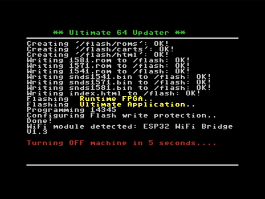
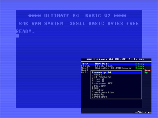
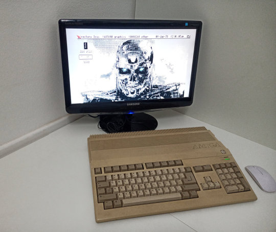
Firmware version 3.12a - for All Platforms: U2, U2+, U2+L, U64 and U64E2!
4 notes
·
View notes