#heterogeneous multi-core processor
Explore tagged Tumblr posts
Visit Tumblr Blog
Explore Tumblr blogs with no restrictions, modern design and the best experience.
Last Seen Tumblr Blogs


Fun Fact
Tumblr was created by web developers David Karp and Marco Arment.
Text
FinFET Technology Market Size Elevating Semiconductor Performance to New Heights
The FinFET Technology Market Size marks a significant milestone in semiconductor fabrication, offering higher performance, lower power consumption, and enhanced scalability compared to traditional planar transistors. With devices shrinking to sub-10 nm nodes, the introduction of FinFETs—transistors featuring a 3D fin structure—has become pivotal for sustaining Moore's Law. These advancements are redefining computing, cellular, automotive, and edge AI applications.
According to Market Size Research Future, global FinFET technology is projected to grow significantly by 2030, driven by increasing demand for high-performance ASICs, 5G infrastructure, and AI accelerators. The shift toward smaller process nodes and energy-efficient designs continues to fuel investment across foundries and OEMs.
Overview of FinFET Technology
FinFET (Fin Field-Effect Transistor) represents a 3D transistor family designed for low leakage and efficient switching at nanometer-scale nodes. By wrapping a thin silicon fin around the gate, FinFETs improve electrostatic control and reduce short-channel effects—critical for modern chip performance.
You'll find FinFETs at the core of system-on-chip (SoC) architectures powering smartphones, high-speed computing, networking hardware, and high-throughput mobile devices. Applications span from Qualcomm's Snapdragon processors to Nvidia’s Ampere GPUs, as both industries prioritize performance-per-watt and thermal limits.
Key Growth Drivers
Advanced Process Node Demand The continuous scaling to 7 nm, 5 nm, and beyond requires FinFETs to maintain channel control, reduce leakage, and boost transistor density.
5G and Networking Infrastructure Infrastructure equipment—like RF front-end modules and baseband SoCs—rely on FinFETs to support high frequencies and low power under elevated thermal loads.
AI Accelerators & Edge Compute FinFETs offer the transistor scaling needed to maintain performance gains in data centers and energy-efficient edge AI processors.
Automotive and Industrial Electronics With automotive electronics requiring high reliability and low power, FinFET integration in ADAS, radar, and EV power components is rising sharply.
Market Size Segmentation
By Node Range: 14 nm & below / 10 nm–7 nm / 5 nm and below
By Transistor Type: High Performance (HP), Low Leakage (LO), High Voltage (HV)
By End‑User: Smartphones, Data Centers, 5G Infrastructure, Automotive, Defense & Aerospace, Consumer Electronics, Industrial IoT
Regional Dynamics
Asia-Pacific leads due to TSMC, Samsung, and Chinese foundries aggressively ramping advanced nodes.
North America excels in design leadership through companies like Intel and Nvidia, including advanced integration of FinFETs in HPC and AI chips.
Europe focuses on automotive-grade FinFETs, with contributions from Infineon and STMicroelectronics in the energy and mobility sectors.
Key Industry Players
TSMC – Dominant pure-play foundry with leadership in high-volume 5 nm and 3 nm FinFET production.
Samsung Foundry – Offers advanced FinFET nodes and innovative packaging through SoC integration.
Intel – Transitioning to FinFET and gate-all-around architectures in its IDM 2.0 strategy.
GlobalFoundries, UMC, and SMIC – Deliver mature FinFET nodes for automotive, industrial, and mid-range SoCs.
Cadence, Synopsys, Mentor (Siemens) – Provide EDA tools for FinFET-based design, modeling, and verification.
ARM, Qualcomm, Broadcom, Nvidia – Utilize FinFET technologies in their SoC portfolio.
Emerging Trends
Gate-All-Around (GAA) Evolution – Next-gen FETs transition from FinFET towards GAA structures (e.g., nanosheet), extending device scaling.
2.5D/3D Chiplets & Heterogeneous Packaging – Integrating FinFET chips via advanced interconnects for modular, multi-die systems.
Beyond FinFET – Research into nanosheet, nanowire transistors, and monolithic 3D stacking is progressing rapidly to sustain scaling.
AI/ML for Process Control – real-time analytics optimize yields and lower defects in FinFET production.
Challenges Ahead
Rising manufacturing costs at sub-5 nm nodes, requiring ROI over large orders.
Thermal management and interconnect resistance, demanding advanced packaging materials and cooling solutions.
Design complexity, requiring sophisticated EDA tools and IP for timing and variability control.
Geopolitical constraints and supply chain uncertainties necessitating diversification and capacity investment.
Future Outlook
FinFET technology will remain dominant through the 2025–2028 horizon, enabling cutting-edge applications in AI, 5G, and edge computing. The transition to GAA and further miniaturization promises continued performance gains. With increasing investment in specialized FinFET fabs and design platforms, this evolution supports the growing demands of intelligent, connected devices.
Related Insights
Explore adjacent technology fields shaping chip innovation:
Radar Lidar Technology for Railway Applications Market Size
Quadruped Robot Market Size
Oxygen Gas Sensor Market Size
E‑Tailing Solution Market Size
Consumer Electronics Mini LED Market Size
D‑Shaped Connector Market Size
Debris Extraction Tool Market Size
Diaper Attachment Sensor Market Size
Digital Holographic Display Market Size
Digital Photo Printing Market Size
Discrete Graphics Microprocessor and GPU Market Size
Diving Compressor Market Size
Explosion Proof Mobile Communication Device Market Size
0 notes
Text

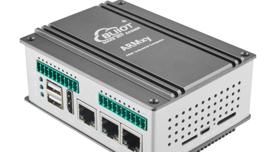
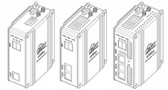
Launched New ARM Embedded Industrial Computer with RK3562J for ARMxy Series
The BL370 series is powered by the industrial-grade Rockchip RK3562/RK3562J processor, featuring a multi-core heterogeneous architecture with a quad-core ARM Cortex-A53 and a single-core ARM Cortex-M0, clocked at up to 1.8GHz/2.0GHz. It offers a robust solution with 4GB LPDDR4X RAM and 32GB eMMC storage, along with a rich set of I/O interfaces. The built-in 1 TOPS NPU supports deep learning capabilities, making it ideal for AI-driven applications.

Key Features:
High Reliability and Cost-Effectiveness: The BL370 series is widely used in industrial control, edge computing, AIoT, artificial intelligence, communication management, AGV robots, machine vision, robotics, industrial IoT gateways, energy storage systems, automation control, and rail transportation.
Versatile Connectivity:
Data Acquisition and Control: Supports communication, PWM output, pulse counting, and more.
Video Processing: Capable of 1080P@60fps H.264 encoding and 4K@30fps H.265 decoding.
Wireless Communication: Built-in Mini PCIe interface supports Bluetooth, WiFi, 4G, and 5G modules.
Software and Development Support:
Operating Systems: Linux-5.10.198, Linux-RT-5.10.198, Ubuntu 20.04, Debian 11 (planned), Android 13 (planned).
Development Tools: Docker containers, Node-RED, and Qt-5.15.2 for GUI development.
Industrial Software:
Robust Design for Harsh Environments:
The BL370 series has undergone professional electrical performance design and high/low-temperature testing, ensuring stable operation in extreme conditions with temperatures ranging from -40°C to 85°C and resistance to electromagnetic interference. Its DIN35 rail mounting makes it suitable for various industrial applications.
Typical Application Areas:
Industrial Control
Energy Storage Systems (EMS/BMS)
AIoT and Artificial Intelligence
Smart Manufacturing
Communication Management
AGV Robots
Machine Vision
Edge Computing
Motion Control
Robotics
Rail Transportation
Smart Devices
The BL370 series combines high performance, reliability, and versatility, making it an ideal solution for demanding industrial and IoT applications.
0 notes
Text
Industry trend|Innovation without boundaries, 2024 IoT Star | Avnet, a century-old technology distribution giant
The "2024 'IoT Star' China IoT Industry Annual List" was officially released recently.
Congratulations to Avnet Electronics Technology (Shenzhen) Ltd., a leading global electronic component technology distributor and solution provider, for winning three awards in the "2024 'IoT Star' China Internet of Things Industry Annual List", including the "Top 100 Chinese Internet of Things Companies in 2024", "2024 China Internet of Things Industry Innovative Products List" and "2024 China Internet of Things Industry Outstanding People List".
Company Introduction

Avnet Electronics Technology (Shenzhen) Ltd.
Avnet was founded in 1921 and listed on the New York Stock Exchange in 1959 (stock code: AVT). It is a leading global technology distributor and solution provider, focusing on the distribution of semiconductors, interconnects, passive and electromechanical components, and providing high-quality technical support and services to more than 100,000 customers worldwide.
Over the past century, Avnet has always adhered to its original intention to meet the ever-changing needs of customers. Whether from conception to design, from prototype creation to production, Avnet can provide customers with full support at every stage of the product life cycle.
With its core position in the IoT technology value chain, Avnet can speed up design and supply during product development, thereby helping customers quickly realize revenue. For many years, Avnet has been committed to promoting technological changes for global customers and suppliers. At present, Avnet has branches in 125 countries and regions and ranks among the Fortune 500 companies in the United States.
Avnet Electronics Technology (Shenzhen) Co., Ltd. is a wholly-owned subsidiary of Avnet in China, providing technology and supply chain services to thousands of domestic leading customers. Through a complete ecosystem and a portfolio of design and supply chain services, it supports the entire product life cycle of customers, entrepreneurs and enterprises of all sizes. With deep design and engineering expertise, combined with comprehensive distribution and integration capabilities, Avnet has a unique advantage in meeting the stringent time-to-market requirements of global customers, while helping customers reduce risks and reduce costs.
2024 Business Overview
In 2024, Avnet ranked 157th on the Fortune 500 list in the United States, and achieved revenue of US$23.8 billion in the 2024 fiscal year from July 2023 to June 2024.
In 2024, Avnet actively deployed in multiple industries and achieved significant development. It has carried out in-depth cooperation with partners such as Desay SV, Sifang Co., Ltd., CRRC Zhuzhou Electric Locomotive, Huaqin Technology, Hangzhou Boco Electronics, Anjieli, and Yidingfeng Power. Its business covers a wide range of fields such as automotive electronics, industrial automation, rail transportation, and smart products, and has won many awards and honors with its outstanding technical capabilities and market performance.
The SMARC/OSM standard edge computing module and supporting design solutions launched by Avnet in 2024 provide a new solution for the edge computing field with its excellent performance and innovative design.
The module supports multiple processor platforms of ARM and x86 architectures, and is compatible with single-core, multi-core and heterogeneous processors of Intel, AMD, NXP, TI, Qualcomm, and Renesas. Its computing power can reach up to 50-80TOPS, supports multiple NPUs and multiple PCIe channels, connects to GPU computing cards, and provides optional FPGA AI acceleration technology.
In addition, the module also supports a variety of industrial control buses and protocols, which can meet the large, medium and small computing power requirements of edge AI, and is widely used in medical, industrial control, robotics, AI brain, new energy and other fields.
The design of all modules strictly complies with the international standards of COM/SMARC/OSM interfaces, adopts SmartFlex baseboard design, adapts to a variety of cross-platform computing modules, provides BIOS customization and other development tools, supports multiple operating systems such as Windows and Linux, and meets professional technical certifications in multiple markets.
At the same time, Avnet's Tria™ independent modular embedded computing series solution further expands the application scenarios of this product, using the latest platforms and processors from multiple semiconductor manufacturers such as AMD, Microsoft, NXP, Qualcomm, Renesas, etc., which can achieve rapid development of applications such as the Internet of Things, industrial interconnection and edge computing, providing significant competitive advantages.

List of Outstanding People in China's Internet of Things Industry in 2024

Avnet's Senior Director of Supplier and Product Marketing for China, Cai Zongfu, was recognized in the "2024 'IoT Star' China IoT Industry Annual List" list of outstanding figures.
Since joining Avnet in 2004, Cai Zongfu has accumulated rich experience in multiple key positions such as technology, product lines and team management with his deep R&D and engineering background, demonstrating outstanding leadership and professional talents. Under his leadership, the team has won many honors and awards from semiconductor manufacturers and customers, and has also repeatedly won important awards from within the company, including Avnet's "Asia Star Achiever Award" and Avnet China's "China Best Achievement Award SPM team".
On the personal side, Cai Zongfu won the honor of Avnet China's first "Reginal President Award" in fiscal year 2022, which is a recognition of his leadership and contribution.
With his keen market insights and management capabilities, Cai Zongfu has cultivated talents, empowered teams, and successfully expanded the coverage of multiple semiconductor manufacturers. He not only effectively sorted out the newly introduced semiconductor product lines, but also reintegrated the existing products, which enabled its turnover to grow several times in a few years, with outstanding performance.
In addition, he led the team to provide customers in the fields of industrial interconnection, Edge AI, artificial intelligence, energy applications, etc. with a full range of supply chain services and technical support, helping customers optimize design, procurement, production and delivery, and also using a set of additional services and technical support to successfully help customers expand new businesses to the whole country and even overseas.
Avnet is bringing new breakthroughs in the field of edge computing. We also congratulate Avnet again for winning the "2024 'Internet of Things Star' China Internet of Things Industry Annual List" "2024 China Internet of Things Enterprise Top 100", "2024 China Internet of Things Industry Innovation Product List" and "2024 China Internet of Things Industry Outstanding People List".
This paper is from Ulink Media, Shenzhen, China, the organizer of IOTE EXPO (IoT Expo in China)

0 notes
Text
Intel oneDPL(oneAPI DPC++ Library) Offloads C++ To SYCL
Standard Parallel C++ Code Offload to SYCL Device Utilizing the Intel oneDPL (oneAPI DPC++ Library).
Enhance C++ Parallel STL methods with multi-platform parallel computing capabilities. C++ algorithms may be executed in parallel and vectorized with to the Parallel Standard Template Library, sometimes known as Parallel STL or pSTL.
Utilizing the cross-platform parallelism capabilities of SYCL and the computational power of heterogeneous architectures, you may improve application performance by offloading Parallel STL algorithms to several devices (CPUs or GPUs) that support the SYCL programming framework. Multiarchitecture, accelerated parallel programming across heterogeneous hardware is made possible by the Intel oneAPI DPC++ Library (oneDPL), which allows you to offload Parallel STL code to SYCL devices.
The code example in this article will show how to offload C++ Parallel STL code to a SYCL device using the oneDPL pSTL_offload preview function.
Parallel API
As outlined in ISO/IEC 14882:2017 (often referred to as C++17) and C++20, the Parallel API in Intel oneAPI DPC++ Library (oneDPL) implements the C++ standard algorithms with execution rules. It provides data parallel execution on accelerators supported by SYCL in the Intel oneAPI DPC++/C++ Compiler, as well as threaded and SIMD execution of these algorithms on Intel processors built on top of OpenMP and oneTBB.
The Parallel API offers comparable parallel range algorithms that follow an execution strategy, extending the capabilities of range algorithms in C++20.
Furthermore, oneDPL offers particular iterations of a few algorithms, such as:
Segmented reduction
A segmented scan
Algorithms for vectorized searches
Key-value pair sorting
Conditional transformation
Iterators and function object classes are part of the utility API. The iterators feature a counting and discard iterator, perform permutation operations on other iterators, zip, and transform. The function object classes provide identity, minimum, and maximum operations that may be supplied to reduction or transform algorithms.
An experimental implementation of asynchronous algorithms is also included in oneDPL.
Intel oneAPI DPC++ Library (oneDPL): An Overview
When used with the Intel oneAPI DPC++/C++ Compiler, oneDPL speeds up SYCL kernels for accelerated parallel programming on a variety of hardware accelerators and architectures. With the help of its Parallel API, which offers range-based algorithms, execution rules, and parallel extensions of C++ STL algorithms, C++ STL-styled programs may be efficiently executed in parallel on multi-core CPUs and offloaded to GPUs.
It supports libraries for parallel computing that developers are acquainted with, such Boost and Parallel STL. Compute. Its SYCL-specific API aids in GPU acceleration of SYCL kernels. In contrast, you may use oneDPL‘s Device Selection API to dynamically assign available computing resources to your workload in accordance with pre-established device execution rules.
For simple, automatic CUDA to SYCL code conversion for multiarchitecture programming free from vendor lock-in, the library easily interfaces with the Intel DPC++ Compatibility Tool and its open equivalent, SYCLomatic.
About the Code Sample
With just few code modifications, the pSTL offload code example demonstrates how to offload common C++ parallel algorithms to SYCL devices (CPUs and GPUs). Using the fsycl-pstl-offload option with the Intel oneAPI DPC++/C++ Compiler, it exploits an experimental oneDPL capability.
To perform data parallel computations on heterogeneous devices, the oneDPL Parallel API offers the following execution policies:
Unseq for sequential performance
Par stands for parallel processing.
Combining the effects of par and unseq policies, par_unseq
The following three programs/sub-samples make up the code sample:
FileWordCount uses C++17 parallel techniques to count the words in a file.
WordCount determines how many words are produced using C++17 parallel methods), and
Various STL algorithms with the aforementioned execution policies (unseq, par, and par_unseq) are implemented by ParSTLTests.
The code example shows how to use the –fsycl-pstl-offload compiler option and standard header inclusion in the existing code to automatically offload STL algorithms called by the std:execution::par_unseq policy to a selected SYCL device.
You may offload your SYCL or OpenMP code to a specialized computing resource or an accelerator (such CPU, GPU, or FPGA) by using specific device selection environment variables offered by the oneAPI programming paradigm. One such environment option is ONEAPI_DEVICE_SELECTOR, which restricts the selection of devices from among all the compute resources that may be used to run the code in applications that are based on SYCL and OpenMP. Additionally, the variable enables the selection of sub-devices as separate execution devices.
The code example demonstrates how to use the ONEAPI_DEVICE SELECTOR variable to offload the code to a selected target device. OneDPL is then used to implement the offloaded code. The code is offloaded to the SYCL device by default if the pSTL offload compiler option is not used.
The example shows how to offload STL code to an Intel Xeon CPU and an Intel Data Center GPU Max. However, offloading C++ STL code to any SYCL device may be done in the same way.
What Comes Next?
To speed up SYCL kernels on the newest CPUs, GPUs, and other accelerators, get started with oneDPL and examine oneDPL code examples right now!
For accelerated, multiarchitecture, high-performance parallel computing, it also urge you to investigate other AI and HPC technologies that are based on the unified oneAPI programming paradigm.
Read more on govindhtech.com
#Intelonedpl#oneAPIDPCLibrary#sycl#Intel#onedpl#ParallelAPI#InteloneAPIDPCCompiler#SYCLomatic#fpga#IntelXeonCPU#cpu#oneapi#api#intel#technology#technews#news#govindhtech
0 notes
Text
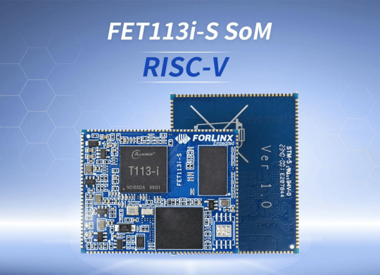
FET113i-S SoM Now Supports RISC-V, Offering a Superior Cost-Effective Solution
FET113i-S is an industrial-grade SoM designed by Forlinx Embedded based on Allwinner T113-i processor. With excellent stability and ultra-high cost performance, FET113i-S SoM has gained wide attention from customers. As a multi-core heterogeneous architecture chip with an A7 core, a RISC-V core, and a DSP core, Allwinner Technology recently released the RISC-V core (XuanTie C906) details for the T113-i, and Forlinx embedded quickly adapted to this development.
1. What is RISC-V?
RISC-V is an open-source instruction set architecture (ISA) based on the principles of Reduced Instruction Set Computing (RISC). It was first introduced by the University of California, Berkeley in 2010 and has since gained significant attention and support from academia and industry worldwide. RISC-V architecture, characterized by its openness, simplicity, and scalability, is emerging as a formidable force in the global semiconductor industry.
2. What Are the Advantages of the T113-i's Risc-v?
High Efficiency and Low Power Consumption
RISC-V architecture follows the principles of reduced instruction set computer, which simplifies the hardware design, improves the execution efficiency and reduces the development cost. The RISC-V cores in the T113-i processor can efficiently perform a wide range of computational tasks while maintaining low power consumption, making it ideal for resource-constrained edge computing environments.
Modularity and Scalability
RISC-V architecture is designed with simplicity and modularity in mind, allowing different instruction set extensions to be chosen based on requirements. RISC-V core in the T113-i processor supports multiple standardized extension instruction sets, such as M (integer multiplication and division), A (atomic operations), and F/D/Q (single/double/quad-precision floating-point operations), enabling flexible combination and addition according to specific application scenarios.
Open Standard and No Licensing Fees
RISC-V is open source, allowing anyone to use and extend it for free, without licensing fees. This greatly promotes technology sharing and innovation, reducing product development costs.
Real-Time Performance
In the T113-i, the A7 core, RISC-V core, and DSP core can run simultaneously, realizing multi-core heterogeneous computing. This design enhances overall system performance and meets diverse application requirements. The RISC-V core, in particular, can accommodate applications with high real-time requirements, ensuring rapid response and processing of real-time data.
3. A Quality Choice for Cost Reduction
Forlinx Embedded FET113i-S SoM, with completed RISC-V core adaptation, is highly competitive in price. Its industrial-grade quality enables it to handle more complex application scenarios, while its comprehensive peripheral interface resources make it both powerful and user-friendly.
FET113i-S SoM's clear advantages, combined with Folinx Embedded's stable supply chain and robust technical support, ensure swift project implementation and market primacy for customers.
Originally published at www.forlinx.net.
0 notes
Text
Exploring the Latest Innovations: A Deep Dive into Hardware Technology
In today's rapidly evolving technological landscape, hardware innovations play a crucial role in shaping the way we interact with the world around us. From cutting-edge processors to groundbreaking peripherals, hardware advancements drive the development of new devices and technologies that enhance our daily lives. In this article, we'll take a comprehensive look at the latest innovations in hardware technology, exploring their impact on various industries and the future of computing.
Advancements in Processor Technology:
Processors are the backbone of modern computing, powering everything from smartphones and laptops to servers and supercomputers. In recent years, there have been significant advancements in processor technology, driven by the demand for faster performance, improved energy efficiency, and enhanced capabilities.
One of the most notable innovations in processor technology is the rise of multi-core processors, which feature multiple processing units on a single chip. These multi-core processors enable parallel processing, allowing devices to perform multiple tasks simultaneously and dramatically improving overall performance.
Moreover, manufacturers are constantly pushing the boundaries of chip design, incorporating new materials and architectures to further boost performance and efficiency. Technologies such as 3D stacking, FinFET transistors, and heterogeneous computing are revolutionizing the way processors are built and optimized for specific tasks.
Evolution of Graphics Processing Units (GPUs):
Graphics processing units (GPUs) have traditionally been used for rendering graphics in video games and multimedia applications. However, in recent years, GPUs have evolved beyond their original purpose and have become indispensable for a wide range of computational tasks, including artificial intelligence, machine learning, and scientific simulations.
The emergence of high-performance computing (HPC) and deep learning has driven the demand for more powerful GPUs capable of handling complex calculations and massive datasets. As a result, GPU manufacturers have been investing heavily in research and development to create GPUs with unprecedented levels of performance and efficiency.
Furthermore, advancements in GPU architecture, such as NVIDIA's CUDA and AMD's Radeon Instinct, have enabled developers to harness the computational power of GPUs for a variety of applications beyond graphics rendering. Today, GPUs are used in data centres, research laboratories, and autonomous vehicles, where their parallel processing capabilities provide a significant performance advantage over traditional CPUs.
The Rise of Edge Computing: Revolutionizing Data Processing and Connectivity
Edge computing represents a significant paradigm shift in computing architecture, offering a decentralized approach that brings processing power closer to the source of data generation. Unlike traditional centralized data centres, edge computing leverages distributed networks of devices, such as routers, gateways, and IoT sensors, to process data locally. This transformative approach offers numerous advantages, including reduced latency, improved scalability, and enhanced privacy and security.
In recent years, the proliferation of Internet of Things (IoT) devices has fueled the rapid growth of edge computing technologies. These devices, ranging from smart thermostats to industrial sensors, generate vast amounts of data in real time. By processing this data locally on edge devices, organizations can extract valuable insights and make critical decisions without the need to transmit data to centralized servers. This not only reduces latency but also minimizes bandwidth usage and ensures faster response times, making edge computing ideal for applications that require real-time data processing, such as autonomous vehicles and industrial automation.
Moreover, edge computing enables organizations to overcome the limitations of traditional cloud-based architectures, particularly in environments with constrained connectivity or stringent data privacy requirements. By processing data locally, edge devices can ensure data sovereignty and compliance with regulatory frameworks, mitigating concerns related to data privacy and security. Additionally, edge computing enhances scalability by distributing computational resources across a network of edge devices, allowing organizations to dynamically allocate resources based on workload demands.
Advancements in hardware miniaturization and low-power design have played a pivotal role in driving the adoption of edge computing solutions. These innovations have enabled the development of compact and energy-efficient edge devices that can be deployed in a wide range of environments, from industrial settings to smart cities. By leveraging embedded processors and storage capabilities, edge devices can perform localized data analysis and decision-making, reducing reliance on centralized infrastructure and optimizing resource utilization.
Furthermore, edge computing holds the promise of enabling new applications and services that were previously impractical or cost-prohibitive. For example, in the healthcare industry, edge computing can support remote patient monitoring and real-time health analytics, improving patient outcomes and reducing healthcare costs. Similarly, in the retail sector, edge computing can enable personalized shopping experiences and real-time inventory management, enhancing customer satisfaction and operational efficiency, the rise of edge computing represents a transformative shift in computing architecture, offering numerous benefits in terms of reduced latency, improved scalability, and enhanced privacy and security. As organizations continue to harness the power of edge computing, we can expect to see a proliferation of innovative applications and services that leverage the capabilities of decentralized computing. By processing data closer to where it is generated, edge computing is paving the way for the next generation of connected devices and applications, driving unprecedented levels of efficiency, agility, and innovation.
Edge computing is a paradigm shift in computing architecture that brings processing power closer to the source of data generation, rather than relying solely on centralized data centers. This distributed approach to computing offers several advantages, including reduced latency, improved scalability, and enhanced privacy and security.
In recent years, there has been a surge in edge computing technologies driven by the proliferation of Internet of Things (IoT) devices and the increasing demand for real-time data processing. Edge devices, such as routers, gateways, and IoT sensors, are equipped with embedded processors and storage capabilities, allowing them to perform localized data analysis and decision-making.
Moreover, advances in hardware miniaturization and low-power design have made it possible to deploy edge computing solutions in a wide range of environments, from industrial settings to smart cities. By processing data closer to where it is generated, edge computing enables faster response times and more efficient use of network bandwidth, paving the way for the next generation of connected devices and applications.
Conclusion:
The latest innovations in hardware technology are driving unprecedented advancements in computing power, efficiency, and scalability. From multi-core processors and high-performance GPUs to edge computing solutions, these innovations are reshaping the way we interact with technology and unlocking new possibilities for innovation across industries.
One of the essential components of hardware innovation is ensuring safety and accessibility in various environments. Zamil Ladders, renowned for its quality and reliability, stands at the forefront of providing robust solutions for working at height. With its range of products including extension ladders, step ladders, and scaffolding, Zamil Ladders ensures that workers can access elevated areas safely and efficiently. Whether in industrial settings, construction sites, or maintenance projects, Zamil Ladders is trusted by professionals worldwide to provide secure access solutions.
0 notes
Text
Amazon FreeRTOS, heterogeneous cores and the all-new Apalis and Colibri iMX8
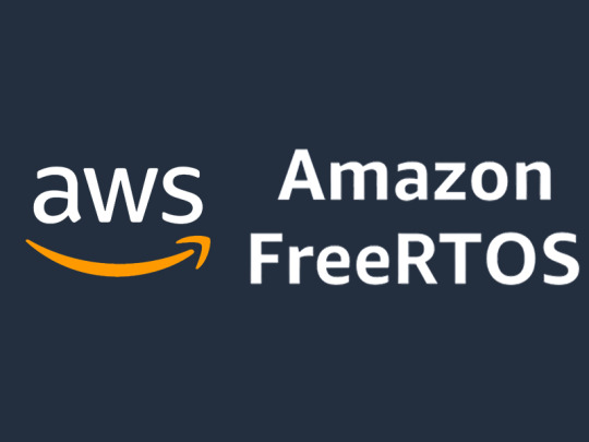
Amazon acquires FreeRTOS FreeRTOS is a real-time operating system kernel for embedded devices. In development since 2003, it is the market-leading real-time operating system, having been ported to more than 40 microcontroller architectures. On November 29, 2017, Amazon acquired FreeRTOS and announced Amazon FreeRTOS (or a:FreeRTOS), a real-time operating system kernel based on FreeRTOS and focused on low-power, connected devices.
Amazon seems to be interested in integrating the most widely used real-time operating system — which, consequently, has a very broad user base — with their cloud services, like AWS IoT Core and AWS Greengrass. After the acquisition, Amazon introduced version 10 of FreeRTOS. Along with new features like cloud and edge connectivity libraries, the kernel license was changed from a modified version of the GNU General Public License (GPL), which the FreeRTOS project used previously, to the more permissive MIT license. This means that FreeRTOS is still a separate product and can be used freely, with or without Amazon services.
Why this is relevant: Heterogeneous Multicore Processing (HMP)
Toradex offers the Colibri iMX7 and Colibri VF61 System on Modules (SoMs) / Computer on Modules (CoMs). These products are based on the NXP® i.MX7 and Vybrid SoC respectively. The processors on these modules feature an Arm® Cortex-A core, usually running an operating system such as embedded Linux; and an Arm Cortex-M4 microcontroller core, which can run bare-metal code or a real-time operating system like FreeRTOS. Here's an outline of use cases:
Control systems: The Cortex-M4 core can be used as a controller for a dynamic system, running, e.g., a PID controller, offloading the Cortex-A core running Linux, which, in turn, could be displaying a human-machine interface.
Data acquisition: On applications that make use of an analog-to-digital converter, the Cortex-M4 core can be employed to acquire data at a high sample rate more easily, also offloading the other core.
An example application using the Toradex Colibri iMX7 System on Module is a self-balancing robot named TAQ. It was developed in partnership with Antmicro and Qt. The robot runs embedded Linux on the Cortex-A7 core, presenting the robot's face animations and sensor data received from the Cortex-M4 core. The Cortex-M4 core runs FreeRTOS, acquiring data from sensors such as an accelerometer and a gyroscope. It uses this data to control the dynamic system, employing a PID controller and a Kalman filter. The cores communicate via RPMsg. A kernel module on the Linux side creates a virtual serial interface which connects to the Cortex-M4; data exchange can be achieved by writing to or reading from this serial device, just as it would be done with a "real" serial device.
The sources for this demo are open and can be found here (Linux side, user interface) and here (Cortex-M4 firmware).
The Toradex Colibri iMX7 was also used on a tablet demonstrating some low-power applications. This video showcases the demo, which features sensor data acquisition and visualization while independently displaying power consumption on a separate LCD display.
Toradex supports and maintains a FreeRTOS repository for its System on Modules. Many peripheral drivers and examples are included and ready to use. Some documentation is available at the Toradex Developer Center showing how you can get up and running with the built-in FreeRTOS examples. Watch our webinars for deeper insight into heterogeneous multicore systems development.
youtube
youtube
What about the future?
On the software side
There are many new players in the RTOS market. In 2016, Wind River Systems and the Linux Foundation launched Zephyr, a real-time operating system also focused on small, connected devices, targeting the IoT market. The Toradex Colibri iMX7 System on Module is officially supported by Zephyr, and development is ongoing.
On the hardware side: the all-new NXP i.MX 8-based Apalis and Colibri SoMs
Toradex has just launched the early access phase of its brand-new System on Module, the Apalis iMX8. This powerful SoM is based on the NXP i.MX 8QuadMax (i.MX 8QM) applications processor, featuring two Arm Cortex-A72 cores, four Cortex-A53 cores and two Cortex-M4 cores. Packed with 4 GB of LPDDR4 RAM and 16GB of eMMC flash storage, it also has built-in dual band Wi-Fi (802.11ac) and Bluetooth (Bluetooth 5-ready). This System on Module is ideal for computer vision applications: there are two integrated Vivante GC7000 GPUs, supporting Vulkan and OpenGL ES.
The two Cortex-M4 cores open up many possibilities: as an example, you can run two different applications or real-time operating systems independently, to balance a data processing application; or use one core for sensor data acquisition and the other for post-processing. The microcontroller cores can also be used as a safety fallback for a graphical display, or to present early boot animations instead of static images.
Toradex presented an Apalis iMX8 demo at Embedded World 2018. Watch this video to check it out, along with some other exciting partner demos.
Soon: Colibri iMX8
The Colibri family is also slated to receive an update: Toradex will soon launch its Colibri iMX8 System on Module. Based on the NXP i.MX 8X, it will also feature a heterogeneous multicore architecture, with a Cortex-M4 core and a Cortex-A35 core running side by side. Stay tuned for more information on this upcoming System on Module!
#Amazon web services#FreeRTOS#Amazon FreeRTOS#System on Modules#heterogeneous multi-core processor#nxp i.mx 8quadmax#NXP i.MX 7#NXP VF61
0 notes
Text
---Newest Flagship Acer R13 13.3" Convertible 2-in-1 Full HD IPS Touchscreen Chromebook - Intel Quad-Core MediaTek MT8173C
—Newest Flagship Acer R13 13.3″ Convertible 2-in-1 Full HD IPS Touchscreen Chromebook – Intel Quad-Core MediaTek MT8173C
Acer Chromebook R13 comes with these high level specs: Mediate MT8173C Core Pilot Quad-Core ARM Cortex-A72/A53 Heterogeneous Multi-Processor, Google Chrome Operating System, 13. 3″ Full HD (1920 x 1080) IPS 10-point multi-touch screen, Integrated Imagination Power GX6250 Graphics, 4GB LPDDR3 Onboard Memory, 64GB emcee, 802. 11ac WiFi featuring 2×2 MIMO technology (Dual-Band 2. 4GHz and 5GHz), .…

View On WordPress
0 notes
Text
---Newest Flagship Acer R13 13.3" Convertible 2-in-1 Full HD IPS Touchscreen Chromebook - Intel Quad-Core MediaTek MT8173C 2.1GHz, 4GB RAM, 64GB SSD, WLAN, Bluetooth, Webcam, HDMI, USB 3.0, Chrome OS
—Newest Flagship Acer R13 13.3″ Convertible 2-in-1 Full HD IPS Touchscreen Chromebook – Intel Quad-Core MediaTek MT8173C 2.1GHz, 4GB RAM, 64GB SSD, WLAN, Bluetooth, Webcam, HDMI, USB 3.0, Chrome OS
Price: (as of – Details) Acer Chromebook R13 comes with these high level specs: Mediate MT8173C Core Pilot Quad-Core ARM Cortex-A72/A53 Heterogeneous Multi-Processor, Google Chrome Operating System, 13. 3″ Full HD (1920 x 1080) IPS 10-point multi-touch screen, Integrated Imagination Power GX6250 Graphics, 4GB LPDDR3 Onboard Memory, 64GB emcee, 802. 11ac WiFi featuring 2×2 MIMO technology…

View On WordPress
0 notes
Text
The BL370 series is powered by the industrial-grade Rockchip RK3562/RK3562J processor, featuring a multi-core heterogeneous architecture with a quad-core ARM Cortex-A53 and a single-core ARM Cortex-M0, clocked at up to 1.8GHz/2.0GHz. It offers a robust solution with 4GB LPDDR4X RAM and 32GB eMMC storage, along with a rich set of I/O interfaces. The built-in 1 TOPS NPU supports deep learning capabilities, making it ideal for AI-driven applications.
Key Features:
High Reliability and Cost-Effectiveness: The BL370 series is widely used in industrial control, edge computing, AIoT, artificial intelligence, communication management, AGV robots, machine vision, robotics, industrial IoT gateways, energy storage systems, automation control, and rail transportation.
Versatile Connectivity:
Data Acquisition and Control: Supports communication, PWM output, pulse counting, and more.
Video Processing: Capable of 1080P@60fps H.264 encoding and 4K@30fps H.265 decoding.
Wireless Communication: Built-in Mini PCIe interface supports Bluetooth, WiFi, 4G, and 5G modules.
Software and Development Support:
Operating Systems: Linux-5.10.198, Linux-RT-5.10.198, Ubuntu 20.04, Debian 11 (planned), Android 13 (planned).
Development Tools: Docker containers, Node-RED, and Qt-5.15.2 for GUI development.
Industrial Software:
Robust Design for Harsh Environments:
The BL370 series has undergone professional electrical performance design and high/low-temperature testing, ensuring stable operation in extreme conditions with temperatures ranging from -40°C to 85°C and resistance to electromagnetic interference. Its DIN35 rail mounting makes it suitable for various industrial applications.
Typical Application Areas:
Industrial Control
Energy Storage Systems (EMS/BMS)
AIoT and Artificial Intelligence
Smart Manufacturing
Communication Management
AGV Robots
Machine Vision
Edge Computing
Motion Control
Robotics
Rail Transportation
Smart Devices
The BL370 series combines high performance, reliability, and versatility, making it an ideal solution for demanding industrial and IoT applications.
0 notes
Text
Industry trend|Snapdragon 8 Extreme Edition is launched: computing power reaches 80TOPS! Edge-side AI sets the mobile phone industry on fire
On October 22, Beijing time, Qualcomm released its new generation flagship mobile phone processor, Snapdragon 8 Elite (hereinafter referred to as Snapdragon 8 Extreme Edition) at the Snapdragon Summit. This processor is said to bring laptop-level functions to smartphones. It is Qualcomm's most powerful and fastest mobile system-on-chip to date.

Qualcomm said that the platform uses the second-generation customized Qualcomm Oryon CPU, Qualcomm Adreno GPU and enhanced Qualcomm Hexagon NPU for the first time to achieve multi-modal generative AI applications on the terminal side. These technologies also enable many other experiences, including imaging functions using the company's powerful AI-ISP, next-generation gaming experience and ultra-fast web browsing.
At the summit, OpenAI CEO Sam Altman, Microsoft CEO Satya Nadella, and Meta CEO Mark Zuckerberg also expressed their support online.

1. Self-developed Oyron CPU, the strongest performance of current smartphones
Public information shows that the Snapdragon 8 Extreme Edition is manufactured using TSMC's 3nm process. Compared with the Snapdragon 8 Gen3, the CPU performance is improved by 45%, the energy efficiency is improved by 44%, and the CPU has a maximum frequency of 4.32GHz, exceeding the MediaTek Dimensity 9400 and Apple A18 Pro.
The Snapdragon 8 Extreme Edition is equipped with a new Oryon CPU. As Qualcomm's "world's fastest mobile CPU", the Oryon CPU does not directly adopt the architecture of computer chips, but consists of two "super cores" with a main frequency of 4.32GHz and six "performance cores" with an operating frequency of up to 3.53GHz, integrating the X80 5G modem RF system.
https://s1.iotexpo.com.cn/ue/24/23/6386529120819322604470021.png
The new Adreno GPU design has also changed significantly, with dedicated memory allocated to each slice, achieving a 40% increase in single-core performance, a 42% increase in multi-core performance, and a 40% reduction in power consumption. It also improves ray tracing performance by 35%.

In addition, Qualcomm has reserved 12MB of memory for the GPU, which reduces the access to system memory during data transmission interaction, and can also reduce power consumption delay and system memory usage.
In terms of network connection performance, the Snapdragon 8 Extreme Edition is equipped with a Snapdragon X80 5G modem, with a peak download speed of up to 10 Gbps and a theoretical maximum upload speed of up to 3.5Gbps. This is a groundbreaking modem that supports 6Rx for smartphones for the first time and is also equipped with a dedicated AI tensor accelerator, which can optimize data transmission speed and reduce latency through AI.
2. Cooperation with Zhipu and Tencent Hunyuan on end-side AI
Qualcomm has been deeply involved in end-side AI for many years. The Qualcomm AI engine based on heterogeneous architecture has successfully implemented large models, AIGC and other applications on the end-side with its performance and flexibility.
The Snapdragon 8 Extreme Edition is equipped with Qualcomm's fastest Hexagon NPU to date, with 80TOPS AI computing power, 46% performance improvement, 45% energy efficiency improvement, and comprehensive improvements in CPU, GPU, memory, etc., which also take the platform's AI performance to a higher level, with a comprehensive AI performance enhancement of 45%.
In the MLPerf BenchMarks test, compared with the third-generation Snapdragon 8, the improvement reached 104% (EDSR super score).
It can be seen that Qualcomm is expanding the capabilities of its AI engine to support multimodal generation tasks. Both the "big cup" and "small cup" multimodal models can run smoothly on its SLM at a speed of up to 70 tokens per second.
In terms of imaging, the Snapdragon 8 Extreme Edition is equipped with an enhanced image signal processor (ISP) and is more deeply integrated with the new Hexagon NPU. This means that taking photos can get more AI capabilities, such as the HDR effect will be taken to a higher level, the skin color of the characters and the color of the sky will be closer to nature, and the autofocus capability will be better. In addition, Qualcomm has also introduced semantic segmentation technology for photos and videos at the chip level, as well as the function of removing objects in videos.

At the Snapdragon Summit, Qualcomm Technologies also announced cooperation with Zhipu and Tencent Hunyuan.
Qualcomm and Zhipu cooperated on the GLM-4V end-side vision model, which was deeply adapted and optimized for inference on the Snapdragon 8 Extreme Edition, supporting a rich multi-modal interaction method. Leveraging the powerful end-side AI performance of the Snapdragon 8 Extreme Edition and the performance optimization brought by the Qualcomm AI software stack to the model, the GLM-4V end-side vision model can run at a high speed of more than 70 tokens/second on the end-side.
The GLM-4V-Mini, GLM-4V-Nano end-side vision model and the GLM-4-9B model will soon be launched on the Qualcomm AI Hub, and commercial mobile phones equipped with the Snapdragon 8 Extreme Edition can support them.
Qualcomm and Tencent Hunyuan have cooperated to implement the terminal-side deployment of the 7B and 3B versions of the Tencent Hunyuan model based on the Snapdragon 8 Extreme Edition mobile platform, further expanding the application and popularization of generative AI technology on the end-side.
In terms of game performance, Qualcomm and NetEase cooperated to create an innovative "Naraka: Bladepoint" mobile game experience based on Qualcomm Snapdragon 8 Extreme Edition chip, using a series of Snapdragon Elite Gaming features, and bringing a new upgraded AI teammate function on the terminal side.
3.Mobile phone manufacturers, new phones are released in succession
Qualcomm revealed that leading OEM manufacturers and smartphone brands such as ASUS, Honor, iQOO, Motorola, Nubia, OnePlus, OPPO, Red Magic, Redmi, realme, Samsung, vivo, Xiaomi and ZTE will release terminal devices equipped with Snapdragon 8 Extreme Edition in the next few weeks.
Not only that, Xiaomi Group Senior Vice President Zeng Xuezhong, Honor CMO Guo Rui, and Samsung Mobile Experience President Lu Taiwen came directly to the press conference to support Qualcomm.
At the Snapdragon Summit, Xiaomi Group Senior Vice President and President of International Department Zeng Xuezhong announced that the Xiaomi 15 series will be the world's first Snapdragon 8 Extreme Edition, and the new phone will be released at the end of this month. It is reported that the Xiaomi 15 series equipped with Snapdragon 8 Extreme Edition has a 29.7% reduction in power consumption and a 3°C drop in temperature at full frame.
Honor CMO Guo Rui showed the real photos of the Magic7 series. The back of the device adopts an octagonal camera Deco design, the middle frame is a metal right-angle edge, and the front is a centered dual-hole screen that supports 3D face recognition + ultrasonic screen fingerprint recognition.

Not only that, terminal equipment manufacturers have sent congratulatory messages and revealed the dynamics of new phones equipped with Snapdragon 8 Extreme Edition:
ASUS Co-CEO Xu Xianyue:
"ROG 9 is equipped with the excellent performance of Snapdragon 8® Extreme Edition mobile platform, integrating innovative terminal-side generative AI and gaming capabilities, bringing changes to consumer experience."
The ROG 9 series includes two models, ROG 9 and ROG 9 Pro. It is reported that ASUS will launch ROG 9 in November 2024 and release the Pro model in the first quarter of 2025.
Zhao Ming, CEO of Honor Terminal Co., Ltd.:
"Our upcoming flagship product, the Honor Magic 7 series, is equipped with Qualcomm Technologies' most advanced Snapdragon 8 Extreme Edition mobile platform. We are very excited to launch the industry's first AI Agent for an open ecosystem, and for the first time introduce the on-device generative AI driven by NPU computing to portraits and games."
Honor will hold a press conference for the Honor Magic 7 and Magic 7 Pro on October 30, 2024. This series of mobile phones will be the first to be equipped with the new Honor MagicOS 9.0 operating system.
Duan Yaohui, senior vice president of OPPO, said:
"OPPO has maintained a close cooperation with Qualcomm Technologies for many years, bringing users many innovative experiences including on-device generative AI. We are very much looking forward to the release of OnePlus 13, which will not only be equipped with the Snapdragon 8 Extreme Edition mobile platform, but also the flagship masterpiece that will open a new decade for the OnePlus brand."
The release of the OnePlus 13 mobile phone is scheduled for 4 pm on October 31. This phone is called OnePlus's "first flagship of the new decade" and is nicknamed "Thirteen Spices" internally.
Xu Qi, Vice President of realme and President of China
"The release of the Snapdragon 8® Extreme Edition mobile platform has once again refreshed the performance boundaries of mobile phone products, injecting unprecedented power into realme's latest flagship products. I believe that the outstanding technical upgrades of the Snapdragon 8® Extreme Edition mobile platform will bring users amazing performance and enable a rich experience across imaging functions and terminal-side generative AI."
realme will release the GT7 Pro this month, with an AnTuTu score of 3.02 million. The GT7 Pro is equipped with a high-specification micro-quad-curved screen of about 6.8 inches, and the display effect is excellent.
Yu Hang, co-founder of Nubia
"As the pioneer of the e-sports gaming phone category, Red Magic has always been committed to breaking through the performance limits and will take it as its responsibility to create professional-quality e-sports equipment for users. The new Red Magic 10 series will be released soon. The series will be equipped with the Snapdragon 8® Extreme Edition mobile platform and will officially meet with everyone in November. We firmly believe that with the excellent performance of the Snapdragon 8® Extreme Edition, the Red Magic 10 series will bring consumers an unprecedented gaming experience."
Shi Yujian, senior vice president and chief technology officer of vivo
"With the new slicing architecture and other rich features from Qualcomm Adreno GPU, iQOO 13 will bring consumers an excellent new gaming experience and stunning visual effects. We will work together to promote the e-sports experience into a new era."
iQOO 13 will be the first to be equipped with Qualcomm Snapdragon 8 Extreme Edition processor, and equipped with a 2K ultra-narrow edge straight screen with a refresh rate of 144Hz. It is estimated to be released in China in October and land in the Indian market on December 3.
Luo Wei, Vice President of ZTE and Director of Product Center of ZTE Terminal Business Unit
"We are pleased to announce that the nubia Z series flagship phone based on the Snapdragon 8 Extreme Edition mobile platform will be launched soon. This new phone not only continues nubia's professional imaging genes, but also upgrades performance, design and system experience."
Lu Weibing, Partner, Group President, and President of Mobile Phone Department of Xiaomi Group
"The Xiaomi 15 series will soon launch the flagship "core king" of Snapdragon 8 Extreme Edition, bringing amazing performance, excellent energy efficiency and terminal-side multi-modal generative AI application support, opening a new era of terminal-side generative AI." It is reported that Xiaomi will launch the Xiaomi 15 series on October 28.
At this Qualcomm Snapdragon Summit, Qualcomm CEO Cristiano Amon spent a lot of time in his speech to explain Qualcomm's understanding of AI trends. In his view, AI capabilities will become the most important user experience on future mobile phones. Users will gradually abandon traditional apps and experience more AI applications, and the status of traditional killer applications will also be threatened.
"Qualcomm is transforming into an interconnected computing company dominated by AI processors." - Today, the Snapdragon 8 Extreme Edition has built a broad stage, and the war for AI mobile phones has officially begun.
This paper is from Ulink Media, Shenzhen, China, the organizer of IOTE EXPO (IoT Expo in China)
0 notes
Text
Dell PowerEdge HS5620 System’s Cooling Design Advantages

Cloud Scale PowerEdge HS5620 Server
Open-source, optimised, and simplified: To reduce additional expenses and overhead, the 2U, 2 socket Dell PowerEdge HS5620 offers customised configurations that grow with ease.
Specifically designed for you: The most widely used IT applications from cloud service providers are optimised for the Dell PowerEdge HS5620, allowing for a quicker time to market.
Optimisation without the cost: With this scalable server, technology optimisation is provided without the added cost and hassle of maintaining extreme settings.
You gain simplicity for large-scale, heterogeneous SaaS, PaaS, and IaaS datacenters with customisation performance, I/O flexibility, and open ecosystem system management.
Perfect for cloud native storage intensive workloads, SDS node virtualisation, and medium VM density
Image Credit To Dell
For quicker and more precise processing, add up to two 5th generation Intel Xeon Scalable processors with up to 32 cores.
Utilise up to 16 DDR5 RDIMMS to speed up in-memory workloads at 5600 MT/sec.
Options for storing include:
Eight x 2.5 NVMe are possible.
12 × 3.5 SAS/SATA maximum
16 x 2.5 SAS/SATA maximum
Open Server Manager, which is based on OpenBMC, and iDRAC are two solutions for embedded system management.
Choose from a large assortment of SSDs and COMM cards with verified vendor firmware to save time.
PowerEdge HS5620
Cloud service providers are the target market for open platform, cloud-scale servers.
Open, optimised, and simplified
The newest Dell PowerEdge HS5620 is a 2U, two-socket rack server designed specifically for the most widely used IT applications by cloud service providers. With this scalable server, technology optimisation is provided without the added cost and hassle of maintaining extreme settings. You gain simplicity for large-scale, heterogeneous SaaS, PaaS, and IaaS datacenters with customisable performance, I/O flexibility, and open ecosystem system management.
Crafted to accommodate your workloads
Efficient performance with a maximum of two 32-core 5th generation and 32-core 4th generation Intel Xeon Scalable processors per socket.
Use up to 16 DDR5 RDIMMS to speed up in-memory applications up to 5200 MT/sec.
Support heavy storage workloads.
Personalised to Meet Your Needs
Scalable configurations.
Workloads validated to reduce additional expenses and overhead.
Dell Open Server Manager, which is based on OpenBMC, offers an option for open ecosystem administration.
Choose from a large assortment of SSDs and COMM cards with verified vendor firmware to save time.
Cyber Resilient Design for Zero Trust Operations & IT Environment
Every stage of the PowerEdge lifecycle, from the factory-to-site integrity assurance and protected supply chain, incorporates security. End-to-end boot resilience is anchored by a silicon-based root of trust, and trustworthy operations are ensured by role-based access controls and multi-factor authentication (MFA).
Boost productivity and expedite processes through self-governing cooperation
For PowerEdge servers, the Dell OpenManage systems management portfolio offers a complete, effective, and safe solution. Using iDRAC and the OpenManage Enterprise console, streamline, automate, and centralise one-to-many management. For open ecosystem system management, the HS5620 provides Open Server Manager, which is based on OpenBMC.
Durability
The PowerEdge portfolio is made to manufacture, deliver, and recycle items to help cut your operating expenses and lessen your carbon impact. This includes recycled materials in their products and packaging as well as smart, inventive alternatives for energy efficiency. With Dell Technologies Services, they even simplify the responsible retirement of outdated systems.
With Dell Technologies Services, you can sleep easier
Optimise your PowerEdge servers with a wide range of services, supported by their 60K+ employees and partners, available across 170 locations, including consulting, data migration, the ProDeploy and ProSupport suites, and more. Cloud Scale Servers are only available to a limited number of clients under the Hyperscale Next initiative.
An in-depth examination of the benefits of the Dell PowerEdge HS5620 system cooling design
Understanding the systems’ performance in each test situation requires analysing their thermal designs. Servers use a variety of design components, such as motherboard design, to keep computers cool. Sensitive components can be prevented from overheating one another by being positioned on the motherboard. Fans also help to maintain airflow, and a well-designed chassis should shield components from hot air. They look at these design components in the Supermicro SYS-621C-TN12R and Dell PowerEdge HS5620 servers below.
The Supermicro SYS-621C-TN12 motherboard configuration that they examined. They also added component labels and arrows that display the direction of the airflow from the fans; blues and purples represent colder air, and reds, oranges, and yellows represent hotter air.
Motherboard layout
The positioning of the M.2 NVMe modules on the Supermicro system’s motherboard presented special challenges. For instance, because the idle SSD was situated immediately downstream of a processor that was under load in the second and third test situations, its temperature climbed as well. Furthermore, the power distribution module (PDU) connecting the two PSUs to the rest of the system did not have a dedicated fan on the right side of the chassis. The Supermicro design, on the other hand, depended on ventilation from the fans integrated into the PSUs at the chassis’ rear.
The BMC recorded a PSU failure during the second fan failure scenario, despite the fact that they did not see a PDU failure, highlighting the disadvantage of this design. On the other hand, the Dell PowerEdge HS5620 motherboard had a more complex architecture. Heat pipes on the heat sinks were employed by processor cooling modules to enable more efficient cooling. Because the PDU was built into the motherboard, the components’ ventilation was improved. Both a Dell HPR Gold and a Dell HPR Silver fan were used in the setup they tested to cool the parts of the PDU.
Summary
Stay cool under pressure with the Dell PowerEdge HS5620 to boost productivity. Elevating the temperature of your data centre can significantly improve energy efficiency and reduce cooling expenses for your company. With servers built to withstand both elevated ambient temperatures and high temperatures brought on by unanticipated events, your company can keep providing the performance that your clients and apps demand.
A Dell PowerEdge HS5620 and a Supermicro SYS-621CTN12R were subjected to an intense floating-point workload in three different scenario types. These scenarios included a fan failure, an HVAC malfunction, and regular operations at 25°C. The Dell server did not encounter any component warnings or failures.
On the other hand, in the last two tests, the Supermicro server had component failures and warnings in all three scenario types, which made the system unusable. After closely examining and comparing each system, they concluded that the motherboard architecture, fans, and chassis of the Dell PowerEdge HS5620 server had advantages for cooling design.
In terms of server cooling design and enterprises seeking to satisfy sustainability goals by operating hotter data centres, the Dell PowerEdge HS5620 is a competitive option that can withstand greater temperatures during regular operations and unplanned breakdowns.
Read more on govindhtech.com
#DellPowerEdgeHS5620System#CoolingDesignAdvantages#cloudservice#5thgeneration#XeonScalableprocessors#intel#DDR5RDIMMS#dell#PowerEdge#rackserve#IntelXeonScalableprocessors#DellTechnologies#motherboarddesign#NVMemodules#motherboard#coolingdesign#technology#technews#news#govindhtech
1 note
·
View note
Text
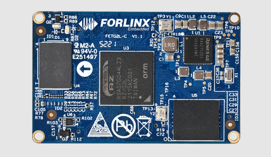
Introducing the FET-G2LD-C System on Module (SoM) powered by the high-performance Renesas RZ/G2L processor! 🚀 Featuring a Cortex-A55 CPU, Mali-G31 GPU, and a variety of display interfaces, this SoM is perfect for industrial, medical, and transportation applications. Operating at industrial-grade temperatures from -40°C to +85°C, it's built to withstand harsh conditions.
0 notes
Text
Mediatek Dimensity 900: A 6nm 5G Chipset
MediaTek has launched its new Chipset. This is a mid-range chipset, but it is a flagship-level chipset. Mediatek announced a game-changing processor. It is said that this processor is more powerful than the Qualcomm mid-range processor. Mediatek announced Dimensity 900 5G chipset on May 13.
It brings excellent performance improvements to 5G mobile devices. Mediatek has launched its Dimensity series for a powerful processor. It has various series like 700, 800, 1000, and more. The Dimensity series is based on a 5G chipset.
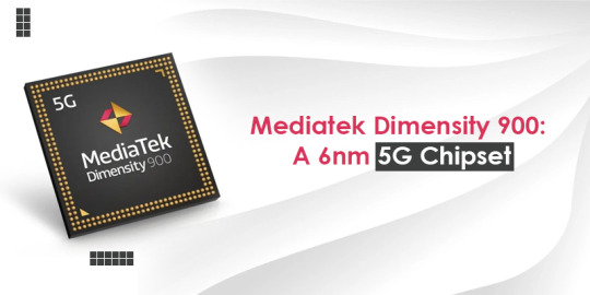
Dimensity 900
The MediaTek Dimensity 900 processor is designed to capture every detail in all environments. It has an exceptional 4K HDR video recording and flagship-grade noise reduction. The processor is integrated with 5G., which gives faster and longer-range connections. This processor provides exceptional power efficiency with natural enhancements. A 6nm fabrication design pushes the boundaries and provides you better battery life.
Specification
The MediaTek Dimensity 900 Processor has two types of CPU. Both CPUs can give the processing speed up to 2.4 GHz. Arm Cortex-A78 and A55 are the CPU in The MediaTek Dimensity 900. The MediaTek Dimensity 900 is an Octa-core processor. It supports Heterogeneous Multi-Processing that makes it more quickly.
The MediaTek Dimensity 900 supports both Memory Type LPDDR4x and LPDDR5
It also supports Storage Type UFS 2.1 and UFS 3.1.
Max Camera support for The MediaTek Dimensity 900 is 108MP, 20MP + 20MP.
You can record videos up to 3840 x 2160. The processor supports various Camera Features such as Hardware video HDR, 3X HDR-ISP, MFNR, 3DNR, AINR, Hardware Depth Engine. It supports multiple Cellular Technologies like 2G / 3G / 4G / 5G Multi-Mode.
The maximum downloading speed on The MediaTek Dimensity 900 processor is 2.77Gbps. It supports Wi-Fi version 6 (a/b/g/n/ac/ax) that provides a better connectivity. It also comes with Bluetooth Version 5.2.
The MediaTek Dimensity 900 has an Arm Mali-G68 MC4 GPU type. The Maximum Display Resolution is 2520 x 1080, and Max Refresh Rate is120Hz. This is a next-generation level processor.
Features
Mediatek Dimensity 900 includes many cutting-edge technologies. Mediatek Dimensity 900 provides a better and faster speed to the devices. We have listed some of the features for the Mediatek Dimensity 900.
Big Cores
MediaTek brings the Arm Cortex-A78 CPU cores to mid-range 5G smartphones With the Dimensity 900 processor. CPUs deliver exceptional performance for more active app response, faster FPS, and better connectivity.
The Arm Mali-G68 GPU features all the more significant G88, but with a design optimized for power capability, extending battery life. It will provide mobile gamers some additional power.
Flexible Memory and Storage
Mediatek Dimensity 900 supports LPDDR5 or LPDDR4X memory, UFS 3.1, or UFS 2.2 storage. Smartphone companies can choose either of them. It is the only chip to flexibly support maximum memory and storage criteria without expecting a platform redesign.
4K HDR Video Engine
Mediatek Dimensity 900 processor has a unique 4K HDR video recording engine. The processor is Combined with noise reduction techniques. These noise reduction techniques are 3DNR and MFNR. Mediatek Dimensity 900 chip enables exceptional visuals in 4K HDR video capture.
Mediatek Dimensity 900 Supports the latest 108MP main cameras with multi-camera trays. This processor provides additional powers to users. They can click photograph more detailed than the previous generation of Dimensity chipsets.
Artificial Intelligent Camera
Mediatek Dimensity 900 processor Meets the next generation demands. It supports the 4K HDR video and single-camera AI. The Mediatek Dimensity 900 processor provides an actual AI processing unit. It deals with ultra-efficient INT8, INT16, and accurate FP16 capabilities. That is helpful for Artificial Intelligent camera experiences.
Dual 5G SIM
Mediatek is a dual SIM leader since 2008. It is now providing dual 5G SIM to mid-range 5G smartphone users with Mediatek Dimensity 900. Users will have access to VoNR call services from both connections whenever they need it with 5G stand-alone.
Faster 120Hz Display
Mediatek Dimensity 900 supports a 120Hz display refresh rate. It will provide a supremely smooth experience to users and gamers. It will be beneficial for both. Users can feel smooth scrolling through web pages and articles. Smartphone brands can offer attractive smartphones with high-resolution Full HD+ displays and ultra-fast touch response.
Wi-Fi 6
Mediatek Dimensity 900 supports Wi-Fi 6. The 2×2 MIMO gives users a quick and reliable connection. The wireless connectivity is more powerful. It uses a smaller platform size than the other processors out in the market.
Conclusion
The Mediatek Dimensity 900 has been launched today. It is a flagship-level processor that is available at mid-range. This is one of the powerful 5G processors compared to some Qualcomm snapdragon 5G processors. It brings excellent performance improvements to 5G mobile devices. Mediatek Dimensity 900 is a premium tech. It is bringing Wi-Fi 6 to the mid-range world. Mediatek Dimensity 900 powered devices may launch in Q1 2022.
Source: https://discussionstech.com/blog/mediatek-dimensity-900-a-6nm-5g-chipset/
0 notes
Text
Acer Chromebook R 13 Convertible CB5-312T-K40U, 13.3-inch Full HD IPS Touch, MediaTek MT8173C, 4GB LPDDR3, 64GB eMMC
Acer Chromebook R 13 Convertible CB5-312T-K40U, 13.3-inch Full HD IPS Touch, MediaTek MT8173C, 4GB LPDDR3, 64GB eMMC
Price: (as of – Details) Acer Chromebook R13 CB5-312T-K40U comes with these high level specs: Mediate MT8173C Core Pilot Quad-Core ARM Cortex-A72/A53 Heterogeneous Multi-Processor, Google Chrome Operating System, 13. 3″ Full HD (1920 x 1080) IPS 10-point multi-touch screen, Integrated Imagination Power GX6250 Graphics, 4GB LPDDR3 Onboard Memory, 64GB emcee, 802. 11ac WiFi featuring 2×2 MIMO…

View On WordPress
0 notes