
ChipEdge was started in October 2012 by battle hardened VLSI professionals who identified that there was a huge mismatch in the present and future requirements of the growing VLSI industry in India
Don't wanna be here? Send us removal request.
Statistics
We looked inside some of the posts by your-chipedge and here's what we found interesting.
Average Info
Notes Per Post
3
Likes Per Post
3
Reblog Per Post
0
Reply Per Post
0
Time Between Posts
2 months
Number of Posts By Type
Text
5
Quote
1
Last Seen Tumblr Blogs


Fun Fact
Tumblr.com is the 103rd most visited website in the world.
Text
Verification Vs Validation In VLSI

State of the art SOC designs is so complex that, coming up with a bug-free design is very difficult. So chip design flow incorporates several steps to identify the bugs in the earlier stages as well as, in the later stages.
Verification and Validation, both probe for the correctness of the design against the specification by identifying and localizing the bugs in the system, but at different stages in the design cycle. Verification is a pre-silicon process of checking the functionality of the design by simulating it whereas, Validation is a post-silicon process of finding bugs in a few initially manufactured prototypes in the context of a system.
Verification
Functional verification is the process of demonstrating the functional correctness of an RTL design with respect to the design specifications. Functional verification attempts to check whether the proposed design is doing what it is intended to do. This is a complex task and takes the majority of time and effort in most large electronic system design projects. It is imperative that the design is functionally verified and any potential bug is eliminated at an early stage.
It is very common that more engineers’ time and expense is spent to verify a design than the rest of the steps in the ASIC design cycle. Even with this large expenditure, most designs are first fabricated with several bugs still in them. So here comes the importance of Validation.
Validation
While pre-silicon verification runs the test cases on the design on the simulator, post-silicon validation is executed on a few initial hardware prototypes of the design on the silicon chip in a real environment. This process captures the bugs that are escaped during the RTL Design Verification phase. Validation also checks for the correctness of the design but on the real hardware in an actual working ambiance.
When a design is passed through all the steps in the design cycle, a few initial prototypes are fabricated as test prototypes. These prototypes are mounted on a test board in a real working environment with real test speed. Identifying bugs through validation is a very fast process as compared to the design verification process but it is difficult to debug the design as there is no way to access the internal signals.
1 note
·
View note
Text
What is Unateness in Static Timing Analysis?

Timing Sense corresponds to the functionality of the standard cells. It explains the traversal of a data from the source pin of the gate to its sink pin. Timing sense is also called as unateness of the timing arc.
All the standard cells can be classified based on the unateness they possess. Positive unate, Negative unate and Non-unate are the three types of unateness.
Under the timing section of a standard cell in .lib file, you can find timing sense information.
Positive unate: The rise transition at the source pin causes rise transition or no transition at the sink pin and fall transition at the source pin causes fall transition or no transition at the sink pin.
Standard Cells like AND Gate, OR gate, buffer possess this property.
Consider the truth table of AND Gate:
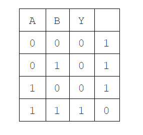
Consider the 1st case of inputs where both A and B are at logic 0 and output is at logic 0. Now consider B is getting transition to logic 1 then the output remains at logic 0 only (no transition). Now let A change to logic 1 then the output also transitions to logic 1.
Negative unate timing arc: The rise transition at the source pin causes fall transition or no transition at the sink pin and fall transition at the source pin causes rise transition or no transition at the sink pin.
Standard Cells like NAND Gate, NOR gate, inverter possess this property.
Consider the truth table of Inverter:
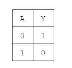
Signal transition on input A makes an opposite transition on the output pin Y.
Non unate: A standard cell which does not possess either of the property is said to be non-unate. XOR and XNOR gates have non-unate timing arcs.
Consider the truth table of XOR Gate :
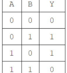
Consider the 1st case of inputs where both A and B are at logic 0 and output is at logic 0. Now consider B is getting transition to logic 1 then the output changes to logic 1. Consider the 3rd row, where output is at logic 1 with A at logic 1 and B at logic 0, now let B change to logic 1 then the output transitions to logic 0. The gate does not possess either of the property. Hence the timing sense of XOR gate is non-unate.
0 notes
Text
How To Choose Frontend Vs. Backend? A guide for Freshers

#VLSI frontend and backend are nothing but two different domains in the field of VLSI. The classification is based on the different steps involved in a typical ASIC design flow. Following diagram shows a typical design flow for an ASIC or SOC.
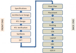
As it shows the design flow starts with a specification document which lists out the technical requirements needed in the chip design. It is followed by translating the specification to Architectural design. The architectural design involves designing the functional blocks and the communication protocol between them and translating them into actual modules that contain FSMs, combinational and sequential circuits etc. The architectural design is then modelled using a Hardware description language like Verilog/VHDL/System Verilog, which is the RTL design stage. The Functional Verification stage starts with a verification plan and a corresponding verification environment which describes and implements the method of proving the design correctness, using different Verification techniques. The design is refined until the HDL model is proved to be meeting the specifications.This stage is followed by Synthesis – a process of transforming the HDL design into a technology specific gate-level netlist, given all the specified constraints and optimization settings. DFT is a structural technique which facilitates a design to become testable after production. All the works till this stage are normally called as the Frontend of VLSI design and are executed by Frontend Engineers.
The next step in the ASIC Design flow is Placement and Routing which involves arranging approximate locations of a set of modules that need to be placed on a layout. Clock tree synthesis is a process which makes sure that the clock gets distributed evenly to all sequential elements in a design to fix the timing violations. This is followed by routing in which exact paths for the interconnection of standard cells and macros and I/O pins are determined.The file produced at the output of the layout is the GDSII (GDS2) file which is the file used by the foundry to fabricate the silicon. Gate level simulations and Static Timing Analysis (a method of validating the timing performance of a design by checking all possible paths for timing violations without having to simulate) are also done to make sure that the gate level design meets the timing requirements for correct design operations. All steps after logic synthesis are performed by Backend engineers and forms the Backend jobs.
Work of a Frontend Engineer
RTL Design/Coding
Synthesis
Functional Verification
DFT
Work of a Backend Engineer
Floor Planning
Placement
Clock Tree Synthesis
STA
Physical Verification
Which one has more career Opportunities?
With the advances being made in technologies like process geometries, feature size and product innovations on a daily basis, there is a constant need to design, develop and re-engineer integrated circuits (ICs). Since electronic products like mobile phones are being released with new features in shorter cycles, there is a healthy demand for qualified VLSI engineers to work on these products. Therefore, there is good scope for a career in the VLSI industry. The important point is that both the domains, front end and back end have their own advantages and have great career prospects. It is completely up to you which one to choose depending on your interest and confidence level, as both offer a great deal of learning and growth.
How to choose?
In order to become a front end engineer, one needs to have good knowledge of HDLs(Verilog/VHDL/SystemVerilog). It will be an added advantage if you have industry related protocol knowledge. So if you have ample digital fundamental knowledge, are fond of HDL coding, love debugging and want to have a sound understanding about the functionality of IC or chip you should definitely go for Front End. With the recent emergence of Artificial intelligence and its application towards VLSI opens up a huge scope for Front end engineers. In order to become a back end engineer, one needs to be well equipped with the concepts of digital electronics, CMOS and Analog Circuits, Scripting knowledge for automation, Hands on Tools for physical design, layout etc. If the above mentioned skills fascinates you then you can opt for Backend and there might be a chance to work in Foundry as well.
Challenges faced by a fresher to get into VLSI industry
Even though VLSI industry is a niche and has lots of career opportunities, on the flip side, industry is currently somewhat less reachable for fresh graduates, compared to other areas due to some particular reasons. Firstly, VLSI or chip design requires a deeper level of knowledge and skills than other electronics related fields .But our Universities are not catering 100% to the VLSI industry requirements. Secondly, VLSI chip design is expensive and requires access to high-cost, specialised electronic design automation (EDA) tools.
How can Chipedge help?
Chipedge offers various courses for fresh graduates both in frontend and backend domains, to choose from. The courses are well structured starting from building a strong foundation by emphasising on fundamental subjects like Digital, CMOS etc. Once the candidate becomes confident with the fundamental knowledge, we impart all the domain specific skills required for the VLSI industry, by giving hands on training on industry standard EDA tools (Synopsys).
1 note
·
View note
Text
The Significant Parameters of the VLSI Training Execution with Innovation to Plan Strategies

Gadgets are fundamentally accomplished by Circuits. Circuits can be partitioned into Discrete Circuits and Integrated Circuits
On the off chance that we can not place everything into an IC and if some instant segments are accessible, we use them to accomplish Electronics Circuits, This is called Discrete. This field is called HARDWARE. It is very well covered in VLSI training institutes in Bangalore. We gather every one of the segments and associate them in a PCB, Since these segments are patched to the PCB and Circuit is imprinted on the board, it will be hard to change. In any case to make an Electronics item, HARDWARE is must. So prerequisite for a HARDWARE Engineer is consistently taught at VLSI design course.
In ICs, three will be three sorts.
1. ASIC - Fixed Circuit manufactured inside Silicon
2. FPGA - Flexible Circuit (Configurable) manufactured inside Silicon
3. µP - Flexible Circuit (Programmable) manufactured inside Silicon
ASIC - Low force, Cheap on high volume, Small in size and Fast . In any case contribution will be immense. Typically large organizations do this action. Requires VLSI (verilog, VHDL, C++, Digital) Knowledge
FPGA - High Power, Cheap on Low Volume, Fast - But take additional time to actualize. Requires VLSI (verilog, VHDL, C++, Digital)
Information
µP - High Power, Cheap, Slow. Simple to utilize. Requires Programming
knowledge(C, C++).
ASIC and FPGA execution is called VLSI and µP usage is called Embedded.
Both VLSI and Embedded fields are having popularity. Since ECE understudies are by and large not getting the hang of programming as part their course work, Industry is leaning toward CSE understudies for Embedded. That is the explanation ECE understudies think that it’s hard to go into Embedded field and feels that no opening for work in Embedded field. Quite of openings for work in embedded field, however ECE understudies can land these positions since they need programming capacity.
Indeed, even VLSI field is tied in with programming; however this field requires Electronics information too. That is the explanation CSE understudies couldn't ready to go into VLSI and industry inclines toward ECE understudies. That is reason ECE understudies consider parcels openings for work in VLSI.
In reality Embedded Job Opportunities are substantially more than VLSI. Since ECE and CSE both go into Embedded, Embedded Job openings searches less for ECE understudies.
Starting today both these fields are having colossal openings for work. It is upto the understudy, how he get ready for these fields during their investigations. On the off chance that you follow our Indian University Syllabus and instructing (a large portion of the colleges), you will turn out as futile with a degree paper and qualified for IT bolster administrations and BPO occupations. Use your time viably. Try not to rely upon your school for Knowledge or Skill on these fields.
As a matter of fact, the inserted frameworks in its beginning times in India. In spite of the fact that I can see it developing at incredibly extraordinary pace!
Discussing VLSI, it's likewise in beginning periods. Umm.. Pause, you can really say that it progress in Indian market is insignificant and its developing at seriously moderate rate. We need better government approaches for the advancement of this field.
You'll discover numerous new businesses in implanted framework yet not a solitary semiconductor plant in India, to the extent no. of chances, Embedded have all the more no. of occupations in India.
Furthermore, if your anxiety is about development, both are almost same.
0 notes
Text
COMBINATION OF ASIC AND VLSI FOR BETTER JOB OPPORTUNITIES

ASIC Design and Verification training empowers the members to make contributions to ASIC (application-specific integrated circuit) corporation. ASIC is designed for a particular utility in preference to going for fashionable cause designing. This designing supports the improvement of embedded structures.
The curriculum is designed to impart the know-how and competencies for RTL (Register Transfer Level) designing and netlist generation. Participants exercise static time analysis (STA) for ASIC layout verification and validating the timing usual overall performance of the layout. The studying curve encompasses SOC designing and moreover specializes in HDL techniques for excessive overall performance designs intended for programmable precise judgment devices.
ASIC Verification Course Assignments & Labs:
Design an easy circuit in Verilog
Verification Environment for a simple layout
Creating Makefile
Final Project
Course Objectives:
Enables a profession jumpstart through developing deep expertise on ASIC Verification
Increase competitiveness via gaining experience with Verification ideas and strategies
Introduce Digital Design ideas and Verilog constructs
Build Verification environment for easy layout in Verilog
VLSI Course
Very-large-scale integration (VLSI) is the technique of making an integrated circuit (IC) with the aid of combining lots of transistors into an unmarried chip. In different words, an IC has many transistors on one chip, at the same time as VLSI has very many transistors on one chip. A present-day VLSI chip is a complicated beast with billions of transistors, hundreds of thousands of logic gates deployed for computation and control.
Engineers manipulate to layout those complicated chips by way of using computer aided design (CAD) tools that take a summary description of the chip, and refines it step-clever to a very last design. Designing a VLSI chip involves steps like logic synthesis, timing evaluation, floor planning, placement and routing, verification, and trying out.
VLSI Course and Its Scope
Select the route primarily based to your interest. If you're proper enough in programming then move for verification. Because in verification you have to deal with system verilog;UVM;OVM and so forth. If your semiconductor physics is powerful then cross for physical design. If you are interested by designing part then pass for memory design/widespread cell design. If you're exact sufficient in Analog then go along with analog layout design.Every discipline has precise significance in ASIC design glide. So, become aware of route and pick the course primarily based on it.
Benefits of VLSI design course
Confidence constructing up for IC Design Methodology
Fare knowledge of Digital Logic Design
Fare knowledge of FPGA Implementation
Experience of BEST learning exercise
Acquire abilities to do better Minor/Major Project
Can participate in numerous national/worldwide opposition and Techfest
VLSI stands for Very Large-Scale Integration. It is the technique of creating an Integrated Circuit (IC) by combining transistors or different devices right into a single chip.ICs are used in distinct forms of digital devices. Your cell smartphone includes ICs. An IC is a circuit in which all or a number of the circuit factors are inseparably associated and electrically interconnected in order that it is considered to be indivisible for the functions of construction and commerce.
0 notes
Quote
What is integrated circuit and what is to know about it?
Integrated circuits are functional electronic circuits consisting of a set of transistors, diodes, resistors, and capacitors, made in the same process, on a common silicon semiconductor substance commonly referred to as a chip. Engineers conduct some process which is known as the DFT process, a defect for testability, to determine the circuit process. Taking the DFT course is not only crucial to test the ability of the integrated circuit, but it will also enhance the creditability of the VLCI.
Classification of integrated circuits
The integrated circuit itself is called a chip and is very small. Most of the external size of the integrated circuit is due to the housing and insert connections to the external terminals.
Linear or analog – The first ones are ICs that produce continuous signals as a function of the signals applied to their inputs. The main function of the analog IC is amplification. This group of integrated circuits can be highlighted the operational amplifiers.
Digital – Circuits that only work with a certain number of values or logic states, which are usually two (0 and 1).
According to their range of integration
The integration range refers to the number of components that the IC contains.
Small Scale Integration (SSI) –These are the ICs with the least components. They can have up to 30 devices per chip.
Medium Scale Integration (MSI) – Corresponds to ICs with several hundred components, and may have 30 to 1000 devices per chip (these circuits include decoders, counters, etc.).
Large Scale Integration (LSI) – Contains thousands of components that can hold from 1,000 to 100,000 devices per tablet. These circuits usually perform complex logic functions such as the entire arithmetic part of a calculator, a digital clock, etc.
Very Large Scale Integration (VLSI) – It is the group of ICs with a number of components comprised between 100 000 and 10 million devices per tablet. They are used in the implementation of microprocessors. This is why to determine the normal process of the chip, DFT in VLSI is very important.
Ultra Large Scale Integration (ULSI) – It is the IC group with over 10 million devices per tablet.
Power Integrated Circuits
Some power integrators have a capsule that is extremely similar to that of power transistors. Some important notes regarding heat sink coupling fins –
· The fins can be fixed to aluminum heat sinks in the same method as power transistors.
· Attach the fins to the case itself (if it is metallic) that contains the circuit.
· The fins can be welded to one of the copper faces of the printed circuit (in case of double side).
· The fins are almost always electrically connected inside the ci to the negative pin of the supply (ground).
1 note
·
View note