
Don't wanna be here? Send us removal request.
Statistics
We looked inside some of the posts by ether4life-blog and here's what we found interesting.
Average Info
Notes Per Post
2
Likes Per Post
2
Reblog Per Post
0
Reply Per Post
0
Time Between Posts
13 days
Number of Posts By Type
Text
2
Last Seen Tumblr Blogs


Fun Fact
Tumblr was created by web developers David Karp and Marco Arment.
Text
#ProgPoW Follow-Up: The Cost of ASIC Design
I was glad to see that IfDefElse published an interesting article “The Cost of ASIC Design” as a response to my previous article. However, I think IfDefElse are not very familiar with ASIC design and have made some inaccuracies in their article.

In their article, IfDefElse state that:
The hashrate of ProgPoW is determined by two factors: the compute core, as well as the memory bandwidth. This is why the variance between Ethash and ProgPoW, as shown below...
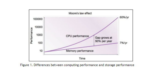
This is not true in ASICs. Although the math function and the merge function have been added into ProgPOW to improve the ratio of visiting computer core and memory in computation, these functions can be achieved by very low costs in ASIC chips. (see EIP 1057 (ProgPoW): Open Chip Design for 1% cost/power increase) As all we know that the performance of computing grows in accordance with Moore’s law, which states that the performance of computing will double every 18 months. However, memory access performance is far behind the developments in computing performance. So memory access performance becomes the bottleneck of the overall performance of the system. This is the so-called Memory Wall as shown in Figure 1.
In the ASIC chip, the computational part is very easy to resolve through design optimization. Whether it is Ethash or ProgPoW, bandwidth of memory access is the bottleneck (refer to EIP 1057 (ProgPoW): Open Chip Design for 1% cost/power increase). The performance of a GPU chip is also limited by the Memory Wall because GPUs are designed for general computing, and not specifically for Ethash or ProgPOW. Actually it is the original intention of Ethash algorithm to limit the computing power by the Memory Wall problem.
In their article, IfDefElse further states that:
The only similarity between ProgPoW and Ethash is the usage of the DAG in global memory. From a computation perspective, Ethash only requires a fixed keccak_f1600 core, and a modulo function. ProgPoW, on the other hand, requires the ability to execute a 16-lane wide sequence of random math, while accessing a high-bandwidth L1 cache. Designing a compute core that can execute the ProgPoW math sequence is significant more difficult than implementing a fixed-function hash like keccak.
From the perspective of an IC engineer, the circuit implementation of a fixed algorithm is the easiest circuit to design. There is no requirement for interaction between hardware and software, no limitation of compatibility or generalization for various computes. The functions in both Ethash and ProgPOW can be simply mapped to a pipelined circuit, with high performance. The logic circuit design can be completed in 2 weeks. However, the GPU is a general-purpose chip that requires interaction between software and hardware, needs to guarantee generalization, requires instruction design, needs architecture design, needs to build a model, etc. It is impossible to complete the design for a GPU chip model within half a year. As for The original Ethash ASICs of Innosilicon or Bitmain, or likely even Linzhi, are built with a successful framework. I believe that it would take only weeks for their ASIC designers to update their Ethash ASIC frameworks for ProgPoW. The design flow, packaging, test boards, and computing boards can all be reused. So it’s quite easy for them to update from Ethash to ProgPoW.
In their article, IfDefElse state that:
First, having 2x the bandwidth will require 2x the compute, so it’s linear scaling, rather than an advantage.
As described earlier in this article, ASICs and GPUs are different. Memory bandwidth, instead of the computing part, is the performance bottleneck for ASICs. However, for GDDR6, even with 8GB devices, an ASIC has a 4x performance advantage over the NV RTX1060, as shown in Table 1.

In their article, IfDefElse state that:
For a chip that has a single functional unit, a smaller die area will be higher yielding than a large die area. That’s not true for modern GPUs. GPU’s today are nearly arbitrarily binnable or recoverable, with a ton of tiny replicated units ignored on defect. As long as each binnable functional unit is small, then the chip yield can be nearly as high — or even higher — than a smaller chip with bigger, functional blocks.
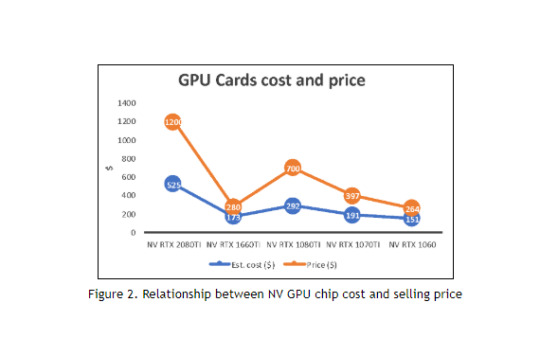
IfDefElse’s above statements is not accurate. Although a large chip with redundant design can repair some chips and improve the yield, only a few of these second grade chips can be saved. Redundancy and repairing are usually for the SRAM, which has simple logical function and repeating cells in structure. For the computing logic units, the circuit is not as simple as SRAM. Adding redundant design means adding redundancy SM cores or something like that. These redundancies will inevitably increase the area of the silicon, thereby increasing the cost. For SRAM, we know that the cost of the redundancy is typically increased by 10%. And not all failures can be fixed by redundant cores. Only pre-calculated failures can be fixed by redundancy logics. BTW, estimating a chip cost from chip area is a basic skill of an ASIC engineer. In Table 1, the cost of GPU cards are estimated based on the silicon area of the chips. The cost of the GPU chips and the price of the corresponding graphics cards are shown in Table 1 and Figure 2. It can be seen that the cost and price are correlated.
In their article, IfDefElse state that:
Low voltage designs can work when the chip consist of only compute, such as a SHA256d ASIC. Integrating other elements like the SRAM (required for ProgPoW data caching), is extremely difficult or impossible to make functional at low voltages.
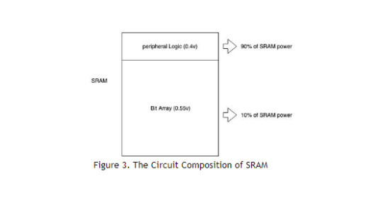
This, too, is inaccurate. The circuit structure of the SRAM is shown in Figure 3. It consists of two parts: Bit Array and peripheral circuit. The working voltage of Bit Array can be reduced to 0.55v but still it only accounts for 10% of the total SRAM energy consumption. The peripheral logic operating voltage can be reduced to 0.4V, and it accounts for 90% of the SRAM energy consumption. Thus, in an ASIC chip, the total reduction in power consumption of the entire SRAM is compatible with the power saved. Therefore, ASIC chips that implement ProgPoW acceleration can significantly reduce power consumption by reducing the voltage. This results in a 4x advantage in terms of energy efficiency over a GPU for ProgPoW, as described in my previous article.
1 note
·
View note
Text
#ProgPoW From the View of an IC Design Engineer
I am an IC design engineer who has also been mining cryptocurrencies since 2014. Although, unlike many other miners from back then, I am not the owner of a large mining farm, I do have a mining setup that makes just enough profit for me to justify the time I spend on it to my wife. Amidst all varying points of views on ProgPoW circulating online, I hope to share those of an IC engineer.
Whether the algorithm is ProgPoW or ETHash, the hashrate is determined by the storage bandwidth of external DRAM. That is,
Hashrate = k*BW
where k is a constant factor and is different for ETHash and ProgPoW
Therefore, to increase the hashrate for ETHash or progPoW, we need to increase the memory bandwidth. In the early years, high-bandwidth memory devices were mainly GDDR5 in graphics cards. Only AMD and Nvidia GPUs could handle such a high-bandwidth memory. So, GPUs from Nvdia or AMD became the most popular for ETHash mining. Now the memory demand for profitably mining ETHash has increased significantly. This demand for high-bandwidth memory has prompted the development of next-generation high-speed memory tech such as GDDR6 and HMB2. In Q4 of 2018, Innosilicon released its GDDR6 IP together with its ETHash mining ASIC. Because of the similarities that exist between the algorithm as well as architecture of ProgPoW and those of ETHash, I believe that Innosilicon’s next ASIC would be tailored for ProgPoW. 3-4 months is sufficient time to design and mass-produce such an ASIC once the parameters of ProgPoW are fixed. I believe that Bitmain is also secretly developing its own GDDR6 IP. Other companies, such as Rambus and eSilicon, have already released IP of GDDR6 and HMB2. I have no doubt that other mining ASIC producers, such as Linzhi and Canaan Creative, will soon adopt GDDR6 or HBM2 in their future generation chips. So, we may see many GDDR6/HBM2 based ASICs for ProgPOW in the near future if ProgPoW is implemented.
Mining ASICs can use optimization methods based on GDDR6 and HBM2. Just an example of these methods is having more GDDR6/HBM2 memory banks in ASICs than GPUs. Take Nvidia's 2080. It uses 8 GDDR6s and operates at 14Gbps, giving it a total bandwidth (BW) of 8*14*32/8 = 448Gbps. According to the bandwidth requirement of ProgPoW, the theoretical hashrate should be
hashrate = BW/64/256 = 27.3Mh/s.
Considering the storage efficiency, the actual value should be 25.5Mh/s. An ASIC producer can use the smaller GDDR6 memory banks to gain cost advantages over GPUs. 16 GDDR6 4GB memory banks can be used to achieve a 2x bandwidth advantage, while maintaining GDDR6 costs at almost the same level. In this case, the available bandwidth is 16*14*32/8 = 896Gbps, and the theoretical hashrate is,
hahsrate = 896Gbps/256/64 = 54.6Mh/s
which gives 2x more hashrate advantage. But the silicon area of 4GB GDDR6 is 50% smaller than that of the 8GB GDDR6. So the price of 4GB GDDR6 should be 60% less than the price of 8GB GDDR6. The total cost of GDDR6 is summarized in Table 1 below.
Let’s look into the internal structure of a GPU chip, such as the Nvidia RTX2080, as shown in Figure 1 from Nvidia.
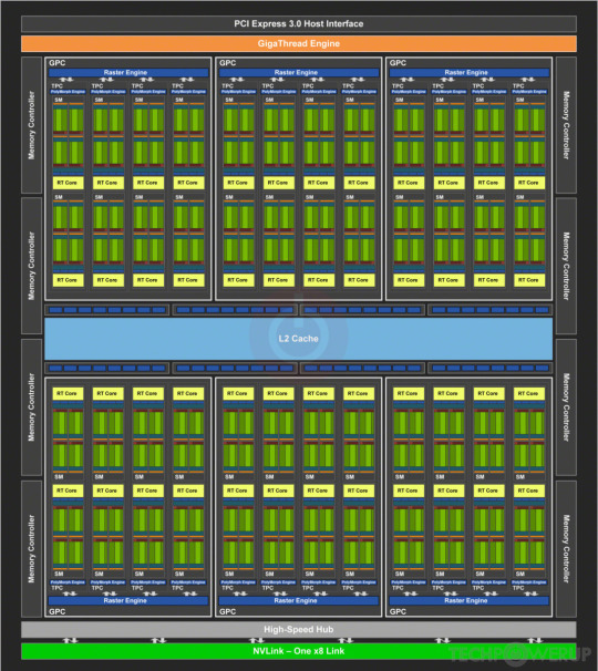
Fig.1: Architecture of Nvidia RTX2080
There are many modules in the RTX2080 chip that occupy a lot of the chip area and are useless for ProgPoW. These include PCIE, NVLINK, L2Cache, 3072 shading units, 64 ROPs, 192 TMUs et. all. An ASIC producer could remove these graphics functions and optimize the same chip area for ProgPOW algorithms, which could reduce the chip area to roughly 1/3rd that of Nvidia’s RTX2080 chip. So, the cost of such an AISC chip would be only 1/3rd that of the RTX2080 because, with the same number of silicon wafers, the number of such ASIC chips that can be produced would be three times more.
And, compared to large chips, small chips have higher yields and lower packaging and testing costs. The yield calculation formula is:
Y = 1/power(1+0.08*die_area)^22.4
For the Nvidia RTX2080 GPU, the die area is 545 mm^2. So the calculated yield of the GPU is 23%. If the area is reduced to 1/3rd, the yield Y will increase by 60%. Low yield will result in a higher cost of the GPU. The cost of such an ASIC would be 1/3*23/60 = 0.13 of that of the GPU. That is a 7.7x more advantage for the ProgPoW ASIC compared to the GPU. Estimating maturity of the GPU, I will keep this advantage limited to 5x for the next calculation. On the system PCB, the ProgPoW ASIC would also have a cost advantage if the ASIC producer were to eliminate the PCIE and complex thermal designs which are required by GPU cards. In an ASIC based mining machine, a large number of ASIC chips and GDDR6, using much simpler and cost-effective heat sink design, would be way more densely packed (and thus shipped). The system cost in a GPU cards may be 50%, but the PCB cost of the ASIC based mining machine can easily be reduced to 30%. I have made the overall cost comparison for GPU and ASICs in Table 1.
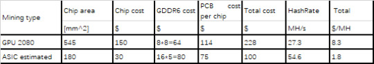
Table 1: the comparison of GPU and ASIC for ProgPOW
As for the power consumption, the GPU would consume much more power as it can only work at the normal voltage, which is usually 0.8V. However, the ProgPoW ASIC’s power consumption can be reduced by reducing the operating voltage. According to Ohm's law, power is proportional to the square of the voltage:
P = U*I = U^2/R
The voltage of ASICs can easily be reduced to 0.4V, which is 1/2 that of GPU’s. Thus, for the same hashrate, the ProgPoW ASIC would consume only 1/4th the power consumed by the GPU. In other words, the ProgPoW ASIC can have an energy efficiency ratio 4x that of the GPU. Such low-voltage ASIC designs are already utilized by ASIC producers in Bitcoin mining machines and there is no reason to believe that they would not be used in ProgPoW ASICs. The same power-saving can also be achieved in LPDDR4x DRAM, which has a lower power consumption than GDDR6. GDDR6 works at 1.35v, while LPDDR4X works at 0.6V, which is less than half that of the GDDR6. So GDDR6 consumes at least 4x more power than LPDDR4x. So an ASIC with LPDDR4x DRAM has a 4x more power efficiency over a GPU with GDDR6. I have shown this in Table 2.
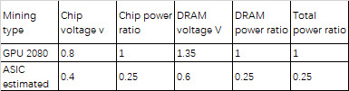
Table 2: Power efficiency comparison of GPU and ASIC with ProgPoW
Furthermore, designing GPUs requires a much higher R&D investment in terms of both human resource and time. Because GPU is a general-purpose acceleration chip, it usually takes about 12 months for a GPU to be designed, fabricated and tested, requiring a lot of hardware simulations and software developing to cover different computing scenarios. But the design and test for ProgPoW's ASICs, are much simpler. A dedicated team of experienced IC designers could take as little as 2 months for design, 6 weeks for fabrication and 2 weeks for testing of ProgPoW ASICs. Thus, it could take only 3 to 4 months for ProgPoW ASICs to be ready for mass production. For ASIC companies, such as Bitmain and Innosilicon, which are already producing ETHash mining ASICs, integrating ProgPoW in their previous designs to produce a ProgPoW ASIC would be even simpler. A GPU producer like Nvidia employs about 8000 people to develop GPUs, which are much more complicated, whereas an ASIC producer like Linzhi only employs a dozen or so people to focus only on ASICs for ETHash mining. The labor costs of these companies company are different by a factor of 100. So ASICs have further advantages in terms of cost and time-to-market than GPU chips.
To summarize, ProgPoW ASICs seems inevitable if ProgPoW were implemented and it would take only 3-4 months for them to hit mass production. Furthermore, they would have at least a 4x advantage in both cost and power efficiency over a GPU for accelerating the ProgPoW algorithm. This would bring us right back to where we started pre-ProgPoW and begs the question: Why ProgPoW or why ASIC-resistance?
1 note
·
View note