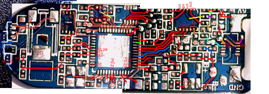
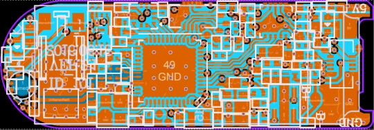
#12 layer pcb stack up
Explore tagged Tumblr posts
Visit Tumblr Blog
Explore Tumblr blogs with no restrictions, modern design and the best experience.
Last Seen Tumblr Blogs


Fun Fact
Tumblr has 4 main sources of revenue.
Text
Learn about the best practices and key considerations for designing a 12-layer PCB stack-up. Viasion provides a detailed guide on layer configuration, signal integrity, and thermal management to help you optimize the performance and reliability of your multi-layer PCBs.
0 notes
Text
ASROCK AMD Radeon RX 9060 XT Challenger 16GB OC GPUs

AMD Radeon RX 9060 XT Challenger Architecture
The ASROCK AMD Radeon RX 9060 XT Challenger 16GB OC graphics card handles 1440p gameplay faster with AMD's RDNA 4 architecture.
AMD RDNA 4 and AMD Radeon RX 9060 XT GPU power it. Next-generation design boosts rendering and performance with unified computing units with advanced ray tracing and AI accelerators.
The card includes 16GB of 128-bit Memory Bus-connected GDDR6 memory. The memory clock is 20 Gbps.
A 2700 MHz game clock and a 3290 MHz boost clock are on board.
Processors and Compute Units: The GPU includes 32 compute units, including third-generation RT and second-generation AI accelerators. Also included are 28 stream processors.
Essential Features and Technologies: ASROCK AMD Radeon RX 9060 XT Challenger
It supports OpenGL 4.6 and DirectX 12 Ultimate.
It supports PCI Express 5.0 via the x16 bus specification.
This lightning-fast gaming design targets improved 1440p performance.
Used AI-powered features and tech AMD FidelityFX Super Resolution 4's ML-powered upscaling and next-generation raytracing generate AI-enhanced graphics.
Used AMD products and supported AMD FidelityFX Super Resolution 4 (FSR 4), which game developers must integrate. AMD does not support FSR on other graphics cards.
AMD HYPR-RX is on Radeon RX 7000 Series GPUs and later. This technology enables AMD Fluid Motion Frames, Radeon Super Resolution, FSR, Radeon Anti-Lag, and Radeon Boost to work together.
Compatible with AMD Smart Access Memory technology, if OEM support is available, with AMD 500 Series or later motherboards with the latest BIOS, AMD Radeon RX 5000 Series GPUs, and Ryzen 3000 Series CPUs (certain models excluded).
An upgraded media engine improves streaming clarity.
Modern ultra-high refresh monitors can employ the updated Radiance Display Engine, which features DisplayPort 2.1a and HDMI 2.1b.
Featuring Future-Ready Technology and longevity.
For optimal AM5 platform performance with AMD Ryzen 9000 Series CPUs.
ASROCK AMD Radeon RX 9060 XT Challenger Resolution and Connectivity:
One HDMI 2.1b, three DisplayPort 2.1a. With a Digital Max Resolution of 7680×4320, it enables up to three screens for multi-viewing. Use HDCP.
Power:
The card needs a 550W PSU with one 8-pin power socket. Power delivery components like Dr. MOS, an integrated power stage for synchronous buck-set down voltage applications, improve thermal performance. It can produce 50A per phase continuously. Additionally, it uses Premium 90A Power Chokes, which have three times the saturation current and greater Vcore voltage than typical chokes.
Cooling system
Dual fans increase cooling efficiency and balance performance and silence. Striped Axial Fans increase airflow with their blade stripe construction and bottom polishing surface. The 0dB Silent Cooling feature turns off the fans at low temperatures for quiet and on when the temperature rises. Cooling includes Ultra-fit and consolidated heatpipes to maximise GPU baseplate contact and heat dissipation.
High-density metal welding isolates pipes and stacked fins, improving heat dissipation. Nano Thermal Paste maximises heat transfer and closes contact gaps. Components heat the heatsink via reliable thermal pads. To protect the GPU die and maximise cooler mounting pressure for thermal efficiency, precise screw torque is employed during construction.
ASROCK AMD Radeon RX 9060 XT Challenger PCB and Hardware:
A sleek metal backplate avoids PCB bending and increases cooling using thermal pads. An LED On/Off Switch turns on or off LED indicators for decoration. The PCB architecture includes a 2 oz copper PCB for lower temperatures and energy efficiency, a matte black PCB with an intriguing colour scheme, and a high density glass fabric PCB to fill layer gaps and prevent humidity-induced electrical shorts.
AMD Radeon RX 9060 XT Challenger Software
User-friendly AMD Software Adrenaline Edition controls performance with trustworthy drivers, real-time AI-powered support, and one-click AMD HYPR-RX optimisation. This software improves gameplay with higher frame rates, less lag, and sharper graphics.
Dimensions and Weight:
Card weighs 645 g and dimensions 249 x 132 x 41 mm.
Price and Availability
The ASRock AMD Radeon RX 9060 XT Challenger 16GB OC graphics card will launch internationally on June 5, 2025, for $349 USD.
#AMDRadeonRX9060XT#AMDRadeonRX9060#RadeonRX9060XT#RX9060XTGPU#AMDRadeonRX9060XTChallenger16GBOC#ASRockAMDRadeonRX9060XT#technology#technews#technologynews#news#govindhtech
0 notes
Text
HDI PCB vs. Traditional Multilayer PCB: What’s the Difference?
As electronic products continue to shrink in size and increase in functionality, designers are faced with new challenges in PCB layout and integration. Two common solutions are Traditional Multilayer PCBs and HDI (High-Density Interconnect) PCBs. Though they serve similar purposes, they differ significantly in design approach, manufacturing complexity, and application scope.
What is a Traditional Multilayer PCB?
A traditional multilayer PCB consists of three or more conductive layers, typically stacked symmetrically with insulating materials (prepreg and core) in between. These boards use through-hole vias to connect all layers and are widely used in industrial, automotive, and consumer electronics.
Standard via types: Through-hole
Layer count: Usually 4–12 layers
Trace width & spacing: Limited by mechanical drilling
Common applications: Power supplies, industrial controllers, communication modules
What is an HDI PCB?
HDI (High-Density Interconnect) PCBs are a more advanced type of multilayer board designed for higher wiring density in a smaller footprint. HDI boards make use of microvias, blind/buried vias, and via-in-pad technologies to achieve compact layouts.
Advanced via types: Microvias, blind vias, buried vias
Layer count: Often 6–20+, including build-up layers
Trace width & spacing: Much finer (can be below 75��m)
Common applications: Smartphones, tablets, medical devices, aerospace electronics
Key Differences
1. Via Technology
Traditional multilayer PCBs rely mainly on mechanical drilling and through-hole vias, which limit routing density.
HDI PCBs use laser-drilled microvias that connect only adjacent layers, allowing finer routing and stacked via structures.
2. Density and Miniaturization
HDI allows more interconnections per unit area, which supports smaller components (e.g., BGAs with 0.4mm pitch).
Traditional PCBs are less suitable for extremely compact or high-pin-count layouts.
3. Manufacturing Complexity
HDI fabrication requires advanced processes like laser drilling, sequential lamination, and high-precision registration.
Traditional multilayer boards follow a simpler, more mature process and are easier to produce in volume.
4. Cost
HDI boards are generally more expensive due to complex manufacturing and tighter tolerances.
Traditional multilayer PCBs are more cost-effective for larger, less space-constrained designs.
5. Signal Integrity
HDI offers shorter trace lengths and better impedance control, making it suitable for high-speed digital and RF signals.
Traditional boards may struggle with signal integrity at very high frequencies.
When to Use HDI or Traditional Multilayer?
Choose HDI PCB when:
Space is extremely limited (e.g., wearables, smartphones)
High-speed or high-frequency signals are involved
You need finer pitch components (e.g., CPU, GPU, DDR)
You aim for thinner, lighter, more compact devices
Choose Traditional Multilayer PCB when:
Size and weight are less critical
The design uses standard components and moderate speeds
Cost is a major concern
Volume production and fast lead time are priorities
Conclusion
Both HDI and traditional multilayer PCBs play important roles in modern electronics. The right choice depends on your application’s complexity, space constraints, performance requirements, and budget. HDI pushes the limits of miniaturization and performance, while traditional multilayer PCBs remain a reliable and economical solution for many mainstream applications.

0 notes
Text
Paying China to reverse engineer for you

In 2016 while visiting Shenzhen factories for a client, I wanted to hunt the markets for my favorite toys, dumb wearables, in order to learn from the design and see what parts are common and cheap. I bought everything I could until I found these veryfit id101′s I liked.


The id101 have a Nordic nrf51 bluetooth chip which is what I use in my work, and which has two open source bluetooth stacks, Apache Mynewt and Zephyr.

After charming my market contact by returning every few days to buy a handful more of them off her, I finally got back to a factory contact on WeChat. They’re made by idoosmart and they agreed to a tour of the factory. I was quite impressed with what I saw. They were clean and had complete testing throughout including water pressure testing every unit as far as I could tell. These guys put out roughly 10k per line per day, and they had several full lines running. I got quotes for something like $9 bucks with no heartrate, and $12 bucks with heartrate in quantities as low as 100. I was paying ~$20 in the markets, and a year later now the id101 can be bought for $20-$40 from any one of many amazon resellers.
I grabbed one of the cheap USB oscilloscopes in the markets and sat at Gee Coffee Roasters to reverse engineer my board. I desoldered all the components and took a picture to mark up while I probed the board.
It wasn’t pretty but got the job done. I identified most of the components and connections.
Printed on board: “id101 ver 2.1 2016.06.13 3716″
Nordic nrf51822 qfaca1 1609ab - Bluetooth LE
hnox ver 2.2 2016.4.19 - HR sensor
Azoteq iqs263a - Captouch Controller
na45e - Battery charge or voltage regulator (?)
"8c630 og155r" sot-23-8? - Erm driver (?)
“2 w6 358411p ba 6" (15pin flex ribbon cable to SSD1306 oled
"1187-02 hxs 2016.09" - 4pin Digitizer 4
"ib 122" LGA-12? maybe Bosch Bma250e accelerometer (?)
Durning this time I finally met Ian and Jin from Dangerous Prototypes who told me about their little known Chinese reverse engineering service. For $80 they’ll reverse engineer a populated 2 layer PCB to Protel in a few days. I handed over $80 and a freshly purchased id101. After a few days Jin got back to me and said it was taking a bit longer. I forgot about it and a few weeks later I had a zip file with some nice pics of a 4 layer (oops) board which presumably slowed them down.


The zip also had the the Protel CAD files. Protel was apparently bought by Altium and is now subsumed into their ~$10k designer tool. I tried to obtain an old copy to run in a VM but it ended up being a huge pain in the ass and so I got bored and put this project down.
Recently, I found out that Altium’s free (though otherwise uncompetitive) online design tool Circuitmaker will actually import Protel files including PCBS. I opened that old zip file in there and found it looking pretty good!
It probably took me a day or two of stitching screenshots, probing nets and marking up images in order to get my jpg. My working rate aside, $80 to get a fully interactive view of the board is worth it in every case I can think of.
Sadly, thats about where I left the id101 project. Find the id101 uploaded to my Circuitmaker account with the zipfile as an attachment. Something I’d love to try next would be to try to actually produce a device based on reverse engineered files.
1 note
·
View note
Text
co2 laser water chiller
The CO2 laser tube is cooled by running or pumping water through the pipe.
This is necessary to extend the life of the tube, or it will overheat and power off quickly and will not run in the end.
CO2 lasers have expensive chillers.
Commercial chillers may be more expensive than low-cost laser cutting machines.
This project provides directions on how to make low cost chillers for CO2 laser cutting machines, whether you are a cheap \"K40\" laser or a beautiful Commercial Full Spectrum Laser.
It will show the construction of the complete chiller system, including an Arduino thermostat enclosed in the acrylic custom laser cutting project box.
The video below shows the action of the thermostat when water cools below 56 degrees Fahrenheit.
Please see my previous article on building a CO2 laser water flow rate monitor and alert.
The chiller system consists of three main parts: the parts list below covers all of these parts and provides low
Source of cost available.
Note, however, that I have used parts that are easily accessible in my small number of parts where possible.
I also used Amazon Prime to save shipping costs if possible, or I found parts available locally.
Fortunately, in San Antonio, Texas, we are fortunate to have the following stores offering the many items needed :(
Note this is not a paid endorsement-
Find similar local shops and support them in your area! )
It\'s also worth noting that when Shack closed many of their stores in San Antonio and component parts, most of my electronic inventory came (e. g.
Switches, wires, Arduino shields, etc. )
You can get a big discount.
Fortunately, even if they didn\'t really take over the manufacturer market, we still have some Radio Shack stores left.
The list of parts below is the system I will record in this article.
However, you should know that I did several attempts before working out this design.
In some photos, you may see the parts you have tried before.
In particular, my first design used a homemade water cooling block and a separate Peltier cooler.
It works, but it\'s not as good as the system I\'m going to introduce.
Component List chillers work by slowly pumping water from a 5 gallon insulated \"beverage cooler\" into a set of \"water cooling blocks\" designed for CPU cooling.
The two blocks are connected with vinyl pipes to increase the time for water to contact the cooling surface of the block.
The water is pumped into one of the blocks from the drink cooler, then pump into the other, and then pump into the drink cooler.
Each water-cooled block is connected to the cold side of peltier (a. k. a. thermoelectric)cooler.
The hot side of the cooler is connected to the CPU cooler with the fan--
One per peltier cooler.
By removing heat from the thermal side of peltier, the cold side is able to freeze the water in seconds.
Therefore, the pump must remain in operation when supplying power to the cooler.
Also, if there is no CPU cooler to take away heat from the thermoelectric cooler, the cooling side will not remain cool.
Please note that the hot side becomes hot enough to cause serious burns.
Do not power it on before connecting to the radiator of the CPU cooler.
Our 92 GPH pump allows as slow pumping speed (
Flow adjustment function).
This increases the time for water to be cooled before being pushed back into the container.
The thermostat is responsible for turning on the pump, thermoelectric cooler and CPU cooler fan.
It also turns on the chassis fan when others are running.
The diagram above illustrates how these parts are stacked and connected together.
The CPU fan 12 volt line and the 12 volt line of the thermoelectric cooler are connected together, but each group remains independent. Use thicker (lower gauge)
Wires for thermoelectric coolers and ground wires.
Each cooler is 90 to 92 watts, so a lot of current is consumed.
I\'m using 22 ad hoc working groups of stranded lines.
It works, but it becomes very warm.
I suggest you use a thicker wire.
Common ground wire can be used.
Radiator compounds are used on each side of the thermoelectric cooler, on each side of the water-cooled block, and on the bottom of the CPU cooler radiator.
As shown in the next step, the CPU cooler will be bolted together to fix everything in place.
They need to be bolted through some kind of material used as a frame.
Once the bolts are connected together, the wires all extend to the wires connected to the thermostat, and after testing everything is OK, some spray
Foam is used for heat insulation around water-cooled blocks.
To improve efficiency, you can add as much insulation as possible.
The following figure shows the complete chiller installed on the 5 gallon beverage cooler.
To assemble the chiller, start with the following sections: prepare for the CPU cooler. The CPU cooler is equipped with legs attached to the plastic holder.
Remove the plastic holder so you only have the metal legs.
There are also screws in the package to connect the legs to the radiator.
Each leg is marked with L or R for proper positioning.
Connect the legs.
The photo below shows the legs at the time of shipment, the brackets on the left and right are removed, how they should be attached to the radiator.
Prepare the installation block. . .
Use a piece of transparent plastic like a bakery container (shown below)
To mark the location of the hole drilled in the mounting block.
Then drill again.
After drilling, cut out the center fit around the thermoelectric cooler and water-cooled block.
One side must be cut (
You can try drilling.
Allow the tube to reach the water cooling block.
I cut with a band saw, but with patience I can use a hacksaw or even a clamp saw or a roller saw.
In the photo to the right below, you will see the bracket/frame I used for the final product.
A piece in the upper left corner is used together with the drill hole to tie that far corner.
Remove the label from the water-cooled block.
A little walk will help.
Assemble the cooler stack with the ready frame and the label removed from the cooling block, and assemble the cooler stack as shown in the chart in the previous step.
To do this, reverse a CPU cooler and apply the radiator compound to the radiator.
Then place the first peltier/thermoelectric cooler Heat side on the radiator.
After that, apply the radiator compound to the top--
Cold side of thermoelectric cooler.
Note: If you do not know which side of the Heat side of your peltier cooler is, please check the specifications it comes with, or when holding the cooler between your fingers, apply the 9 volt battery briefly to the wire with proper polarity.
It\'s just short, or you will get burned.
You will soon find out which side of the heat is.
Next, apply the radiator compounds on both sides of each water-cooled block and stack them together.
Arrange the stack the way you like, but I chose the entrance/exit facing the adjacent side.
I started with the vinyl tube as well, but it does make probably more difficult.
You will notice in the photo below that in one of the tubes I inserted a short section of 1/4 \"O. D.
Copper tubes that help slow the flow slightly.
Once the two water-cooled blocks are stacked together, there are radiator compounds between each layer and at the top, place the second thermoelectric cooler on the top of the stack, under the cold side, up the hot side, and add radiator compounds to its top.
Now put the final CPU cooler at the top of the stack and use enough bolts and nuts to go through the holes on the legs of the CPU cooler at the bottom, through the mounting block holes, and then through the top CPU cooler legs.
Tighten this up but not too tight-
Don\'t crack your peltier cooler!
Fill the foam with some gaps (
Wal-Mart and hardware stores)
To fill the gaps around the water-cooled block.
It is very slow to do so, or it will get out of control.
To protect your table, be sure to put something under the table.
I used some Saran packaging.
Also make sure the wires are not surrounded by foam.
They should go through it, but not buried in it.
To complete the chiller, weld all the black wires to one line of ground.
The wires should be 18 to 24 inch long.
Be sure to use the heat shrink tube to insulate any bare wires.
Connect the ground wire to your 3-pin 1-
Plug pin connector.
Then weld the two red wires of the CPU cooler fan to one wire and attach it to the 3-pin 2-pin
Plug pin connector.
The wires should be 18 to 24 inch long.
Ensure that any bare wires are insulated with a heat shrink tube.
Finally, weld the two red lines on the thermoelectric cooler to a single line between 18 and 24 inch long and weld the other end to 3 pinspin connector.
Similarly, insulated any bare wire with a heat shrink tube. The red wires (pins 2 and 3)
Will be connected to an independent relay in the thermostat.
The other side (
Open side)
The relay will be connected to the 12 V output of the power supply. The black (ground)
The Wire will be connected directly to the power-supply ground.
The installation cooler is done, but you need to find a way to install it on your 5 gallon drink cooler.
This is at least an option.
Maybe you will have the idea of a better way to wrap the cooler.
It needs to be within the range of the thermostat and the tube connected to the water pump inside the beverage cooler.
The photo below shows how I can use 3/16 acrylic and a set of bolts to make a stand that will slide into the cup holder slot on the drink cooler.
The final product probably thermostat unit consists of the following components: Power supply Please note that the 12 V power supply will supply power to all of the following components: I recommend using a power supply capable of 30 a @ 12 V.
Most of the electricity consumed will come from two 92-watt thermoelectric coolers.
First of the build up of Arduino UNO connecting ArduinoThe Seeed Studio relay shield.
In addition to this, we will place a custom shield made of a prototype PCB shielded with ayp82.
Arduino pins are connected as follows: pin 2: push up instantly-
The button switch is connected to the ground on the other side.
Pin 3: push instantly down-
The button switch is connected to the ground on the other side. PINS 4 -
6: Seeed Studio relay ShieldPIN 10 use: connect to the signal line (Yellow or white)
Waterproof digital thermometer.
Be sure to connect it to a pin on the stereo plug.
I chose the pin that was connected to the most extended part of the plug.
When you weld the ip65thermometer line on the stereo jack, make sure it matches.
You also need to run a 4.
7 k ohm resistor from Pin 10 to 5 v line.
Pin A4: SDA connection on the serial LCD backpack board.
Pin A5: the SCL connection to the serial LCD backpack board.
Complete schematic note: the schematic is made using EasyEDA, a free web-based schematic capture program.
I recommend supporting their business so that the service remains free of charge.
Connect the rest. . .
As can be seen from the schematic diagram, the circuit is built on the top of the Arduino shield and connected to the lower layered shield-
Seeed Studio relay shield.
In order to maintain all the modularity, external components--
Chiller and thermometer probe connected via plug
Be able to connect, but it\'s up to you to do this specifically.
You will see from the photo how I did this and it worked well.
In the schematic diagram, the relay is displayed using the label of the relay on the relay shield.
Normally connected in all 4 cases (N. C. )
The Pin is not connected to anything.
It\'s not very important which relay controls which items, but it\'s better to separate them, which will allow you to customize the sketch to change the time to suit your needs.
A small part of the circuit uses AC power.
Of course, the 12 V power supply is powered by an AC power supply.
In addition, the chiller pump is powered by an AC power supply, and the relay controls the power supply of the pump, so it will only operate when the chiller is turned on.
Planning and preparing the project box will make things easier when building blocks and connecting components.
This part of the project is something you should tailor to the material at hand and your own taste.
If you like the project box I built and you can use the LaserCAD file, or.
The platelet file attached to this step, you can match my box in each detail or change the content as needed.
If you use a switch or connector of different sizes, or even if your power cord size is different, you can change the cut-out as needed!
Design box my project box is made of 3/16 \"acrylic.
The box pattern is made using BoxMaker (
BoxMaker will allow you to input the size and thickness of the box and then generate a PDF file containing each panel.
My laser cutter is controlled by LaserCAD and LaserCAD cannot import PDF files, so it is necessary to import PDF files into Inkscape first and then save each panel as a DXF file.
You can import the DXF file into LaserCAD, and then add cuts to external components such as LCD, switch, and chassis fan in LaserCAD.
Use my file if you use the attachment.
The pwj5 file with a laser cutter that supports LaserCAD simply takes note of which colors are enabled and the cutting settings, and adjusts as needed.
Since I made this box in several channels, the current cut setting only reflects the last channel.
There is a file for each panel and a file for making Arduino shelves.
It is also very important to note that some lines marked as cutting lines are not for cutting, but for aligning screw holes, etc.
Usually in.
The Pwj5 files are not selected for these files, or the laser power level of that color is set too low to be cut, usually both.
There is also a group.
Platelet file for each panel.
These are exported from LaserCAD.
You can use.
Open and edit the lt file of the drawing in AutoCAD, or you can use the free online converter to convert the lt file to PDF or other formats used with the laser cutting software.
Feel free to modify the file as you need it, including removing my name and putting your name there!
Arduino shelves have passed-
Holes that match the holes in Arduino Uno, making use of 4-
40 bolts and nuts each.
Assemble each panel cut and appropriate cut into the box and you can now insert the parts and solder wire as needed.
Glue the box with external parts attached to the box panel and wires attached to the shield (see next step)
You can start sticking the box together.
First fix the Arduino shelf on the back panel.
To protect your desktop, be sure to put wax paper or something like that underneath.
In the case that the Arduino shelf is in place, you may want to connect the Arduino and then cement the back plate to the bottom plate.
Cement each remaining panel in place when most convenient, but please note that you prefer to do it in the following order best: by soldering the header pin to the shield, welding the header pin is probably the easiest to start.
If you use a stackable head pin, you can place another Shield on this head pin if you need to expand your circuit.
I used what I had. the non-stackable pins.
In doing so, you may also want to attach a reset button, as you can see in my photo.
No need but I have one so I added it.
Soldering and connecting the LCD thermostat shield requires several wires to be connected from various panels.
If you don\'t mind the time and cost associated with placing a socket, plug or plug pin for the removable cable of the external parts, I highly recommend that you do so.
I didn\'t, largely because I didn\'t want to order them or wait for them to arrive.
Instead, I Weld (long)
With one exception, connect directly to the shield from the connector on the panel.
I happen to have a cable with a connector that fits perfectly with the LCD backpack.
I welded the end of the cable without directly connecting to the shielded connector (
A4, A5, 5 v and GND)
, Then plug the cable into the backpack.
Note: If you order and use the Arducam Series 16x2 LCD package I ordered from Amazon, you first need to weld the backpack to the LCD.
Follow their instructions. -
Or at least test, before welding, make sure that the ground on the backpack matches the ground on the LCD, as you can see in my photo.
The photo below shows 4 wires in the LCD series backpack connected to the shield on pin A4 (SDA)and A5 (SCL)
As well as grounding and 5 V wire connection.
The thermometer connection line is connected to pin 10, and the thermometer connection, the button switch, and the chassis fan power supply. A 4.
7 k ohm resistance is also run from Pin 10 to 5 V pads.
Instant push up
The button switch is connected to pin 2 and the other side is connected to the GND pad.
Similarly, the downward moment pushes
The button switch is connected to pin 3 and the other side is connected to the GND pad.
Pins 2 and 3 are used because they are associated with interrupts 0 and 1 for Arduino.
I also connected a wire from Vin to COM4 on the relay shield.
The NC4 on the relay shield enters the 12 v line of the 80mm chassis fan.
The ground wire of the chassis fan is connected to the GND pad.
This is because I thought of the case afterwards.
I found it quite warm in the box--
Mainly from the power supply.
By adding the chassis fan and powering it only when the cooler is running, the box stays cool.
The photo below shows all of these connections to the label. (
Click or click on it to enlarge it. )
Ardu supplies power to the power jack as shown below.
The red line will be connected to one of the 12 v terminals on the power supply.
The black wire will be connected to one of them-12v (ground)
Terminals on the power supply.
The Jack will be inserted into the Arduino.
Powering the CPU cooler fan, the thermoelectric cooler connects the wires of one of the 12 v terminals on the power supply through RelaysConnect to the NO1 terminals on the relay shield.
Connect another wire from another 12 v terminal on the power supply to the NO2 terminal on the relay shield.
Then connect the 12 v wire from the chiller Jack (3-
Pin audio connector)
COM1 on trunk shield.
Make sure this is connected to the 12 v wire of the CPU cooler fan on the other side of the cable.
This 12 volt terminal can be shared with Arduino power supply.
Connect 12 v wires from the chiller Jack (3-
Pin audio connector)
The red line of the thermoelectric cooler extends to the COM2 on the relay shield.
These relays will be turned on by the thermostat circuit (COM < -> NO)
When the water temperature is lower than the thermostat setting.
Note: I welded the Philmore male terminal (NO. 65-5021C)
For better connection, each wire that goes in and out of relays 1 and 2.
The AC power socket and the main power supply are connected by reconnecting the ground wire, and the neutral ac wire is connected to two power supplies (GND and N)
Direct AC socket with Chiller pump.
Exchange hotline (L)
Connect directly to the power supply (L)
Then arrive at the terminal COM3 on the relay shield.
From the terminal No 3 on the relay shield to the remaining L (hot)
Connection on the AC socket of the chiller pump.
The 80mm chassis fan power supply mentioned in the previous step, you can directly connect the 12 V voltage of one of the power terminals to the COM4, or you can run it from Vin on the shielded PCB like I did.
Again, you can connect the ground wire of the chassis fan directly-
The 12 v terminal on the power supply, or you can connect it to the ground pad on the shielded PCB.
Connect the 12 volt wire of the chassis fan to the NO4 terminal on the relay shield.
Put it all in. . .
Now that all the connections are done, you can connect the shield.
Now you can also put the remaining panel cement in place.
Remember not to cement the top panel!
If something goes wrong, you need to remove it to access the inside!
It will be comfortably installed without cement and the fan Shield will help to remove it.
A prerequisite library for attaching Arduino sketches.
In order to compile and use it, you need to install the following Library: I suggest building a small circuit and sketch to test each component before building a larger circuit, in case there is any change, you need a different library.
If you wish to use my sketch-
Yes, it is connected to this step as a thermostat. ino.
It should work with your Arduino Uno (or clone)
No change if you follow my route. How it works. . .
The thermostat is fairly simple, not unlike the one you use to control the temperature at home.
The LCD displays the current Fahrenheit temperature and degrees Celsius on the first line and the current settings on the second line.
Open the pump and cooler when the water temperature is higher than the set value.
When the temperature drops 1.
Set 75 f ° below and the cooler, pump and fan will all turn off until the temperature is higher than set again.
Input lock because it is difficult to get a clean signal from the Arduino interrupt pin (
Maybe this is my old question.
Used Arduino Uno?
Or maybe because of noise from other parts of the circuit)
, I added the \"set Lock\" feature.
In order to change the thermostat settings, you have to hold down the up and down button for 1 second.
When this is detected, the LCD will display the message \"----UNLOCKED----
\"Enter Temp on the top line, on the second line:\" For 3/4 seconds.
When unlocking, the up and down buttons can be used to increase or decrease the thermostat settings.
If the button is not pressed within 10 seconds, the input lock is restored.
The lock will also be restored if both buttons are pressed and held for 1 second at the same time, but note that if no rebound causes the temperature setting to increase or decrease by one or two, it can be difficult to press both buttons at the same time.
For this reason, you may prefer to have the system re-
10 seconds from line lock by holding the button still.
Read the temperature please read the sketch for all the details of how the code works.
Here, I only emphasize part of it.
In particular, the TemperatureModule class takes advantage of the OneWire 2 Library to read the temperature from the B20 in a digital waterproof temperature probe that meets the protection level.
In the code of the TemperatureModule, the example sketch of OneWire month.
It provides only two methods: Initialization ()
And reading temperature f (). Initialize()
Must be called before the first call to ReadTemperatureF.
ReadTemperatureF will return the temperature in degrees Fahrenheit and will fill a passed variable in degrees Celsius.
After the class is defined, the instance of the TemperatureModule is declared on line 171 of the sketch: You will also notice the g-LCD on line 172
Example of LiquidCrystal_I2C.
Both global objects use macros defined at the top of the file.
These macros also define each Arduino pin used by the sketch: SetupLines 1 to 3 including the library used by the sketch.
In the third line, you will see the inclusion of the EEPROM. h.
This will be used during the setup and after the thermostat settings are adjusted to keep the temperature in the Arduino\'s EEPROM in order to remember it when the power is reset.
The temperature is stored in one byte, allowing the temperature to be set from 35 degrees Fahrenheit to 85 degrees Fahrenheit.
It seems like a reasonable range for us to store simplified values by using a byte. The setup())
In addition to protecting the probe, this tiny modification will allow the thermometer to float underwater.
I\'m thinking of buying a 3/8 or 1/2 copper stick, drilling a hole large enough to insert the probe into it.
The bar will extend to the bottom of the drink cooler and pass the temperature to the probe.
In the end, I think it\'s good enough.
Now it\'s time to place the whole unit near the laser cutter and fill it with distilled water.
If your setting is where water can freeze, you should probably mix distilled water with antifreeze.
Put the lid on it and plug everything in and you should be able to cool the water now.
I tested in a room with an average room temperature of 75 degrees Fahrenheit, and in the case of non-continuous operation, the chiller is easy to maintain 54 degrees Fahrenheit.
While you may know this better than I do, I have read that 56 F is a good temperature to cool the CO2 laser tube. 11.
25 KWHI has already run the chiller
Stop 168 hours-
A whole week. The kill-a-
The reading of the electric energy meter is 11. 25 KWH.
These results are better than expected, although they may not be as good as one would expect.
My current electricity bill is £ 9.
3 cents per kilowatt hour.
Throughout the week, the room temperature averaged 75 degrees Fahrenheit and the laser was used only a few times.
If these variables hold up, my energy cost is about $0. 14/day, or $4. 41 / month.
It\'s about $53. 76 each year.
Your mileage may vary.
I am fortunate to live in a region where the cost per kWh is not as high as the national average.
I recently added a 8,000 watt photovoltaic solar system to my house (
To reduce energy costs--
$700 per month in summer! )
There is no doubt that this will also reduce the cost of running the device.
One thing I noticed is that when the pump of the laser tube is turned on, the water temperature always increases by 1 to 2 degrees, even if the laser is not used.
This is part of the expectation because the tube to the laser tube is not insulated and it is a considerable space --
The temperature moves compared to the path where water passes through the cooler.
But I\'m worried about 620 gallons. per-
The hourly pump I use to pump water through the laser tube is actually heating the water.
I will eventually try to use the outside (non-submersible)
A pump for this purpose, or a smaller submersible pump.
My speedometer shows that I only smoke about 0.
9 liters per minute through the tube.
Is it 54 liters or 14 liters?
26 gallons per hour
I upgraded to a larger pump and tried to increase the flow but could not exceed 0 at all.
9 liters per minute.
It is likely that some heat is caused by a pump that is trying to overcome a direct bottleneck.
While I am afraid of having to cut off and repair another pump AC power cord, I will comment in the future on the effect of using the smaller or outside pump mentioned in the previous step, the large pump I used to water the laser tube caused some warming of the water.
When I run for 30 minutes or more, it\'s clear that the temperature is going up much faster than I expected ---
Up to 5 to 10 degrees.
I have now replaced that pump with an external pump.
The temperature still rises slightly when the pump is running--
Even if the laser is not used, it can be expected because the water flows out of the cooler and is cycled through quite a long pipe and laser pipe, none of which is insulated.
My test shows a temperature rise (Loss of efficiency)
The new pump is only 1 to 3 degrees.
It\'s worth exchanging.
As you can see from the photo, I switched to this small external pump I purchased via Amazon. com.
The pump can be 1. 2 GPH.
It\'s quiet enough not to be a problem.
As a 12 V Pump, I also have to add a 12 V power supply, which is what I have from ATX (computer)power supply.
Since this pump is external and needs water before powering on, I replaced the plug for the 5 gallon drink cooler and delivered the water directly from the cooler to the pump.
I also used \"I\" with a length of 1/4 \". D.
The fuel line from the pump to the flow monitor helps with some insulation.
The flow monitor shows that the pump is able to move about 0.
80 liters per minute through tubing and laser tubes.
This is about 0.
10 liters per minute, less than my oversized submersible pump, but better than the pump that comes with the K40 laser.
Thermostat firmware update I also updated the thermostat firmware.
These changes are needed to solve the problem that the thermometer sometimes reads abnormally.
Now the average of the last 10 readings (Last 10 seconds)
Used to decide to turn the cooler on or off.
Also, any reading 5 degrees or more from the previous reading will be thrown away.
After 10 such conditions, the thermometer will be re-developedinitialized.
This seems necessary because 1-
Wired protocol for reading the thermometer.
The updated Arduino INO file (Thermostat. ino)
Attach to this step.
Although I almost gave up the system after I tried it twice, I was not very happy.
As mentioned, I will try to replace the main pump (
Pump to the laser tube)
To see if I can keep the water cooler during the laser operation, I will add a comment with the results on a future date.
As always, thank you for your comments.
Please also read my 1st articles on CO2 laser water flow speedometer and alarm.
0 notes
Text
PCB Design Engineer Auotmotive Pune
techtosuit - Pune, Maharashtra - Job Description BGA SoC, 8-12 layer board stack up design, impedance matching, differential pair routing, LPDDR4 routing, EMI/EMC, RF Design exposure, Automotive design experience Salary: INR 5,00... from Offres d'emploi - Inde - Optioncarriere http://bit.ly/2AdW9Z6 site=tumblr">
0 notes
Text
PCB Design Engineer Auotmotive Pune
PCB Design Engineer Auotmotive Pune
[ad_1] Gob title: PCB Design Engineer Auotmotive Pune Company: techtosuit Gob description: Job Description BGA SoC, 8-12 layer board stack up design, impedance matching, differential pair routing, LPDDR4 routing, EMI/EMC, RF Design exposure, Automotive design experience Salary: INR 5,00,000 – 15,00,000 P.A. Industry: Automob… Expected salary: Rs.500000 – 1500000 per year Location: Pune,…
View On WordPress
0 notes
Photo

On Sale in Pakistan: https://www.shopperspk.com/product/asus-rog-strix-z390-f-gaming/
ASUS ROG STRIX Z390-F GAMING

Missing Attachment
Description:
Intel Z390 LGA 1151 ATX gaming motherboard with Aura Sync, DDR4 4266 MHz+, dual M.2, SATA 6Gbps, HDMI and USB 3.1 Gen 2
LGA1151 socket for 9th/ 8th Gen Intel® Core™ desktop processors
Aura Sync RGB: Synchronize LED lighting with a vast portfolio of compatible PC gear, including addressable RGB strips
Comprehensive cooling: Onboard M.2 heatsink, water-pump header and a fan-extension header
5-Way Optimization: Automated system-wide tuning, providing AI overclocking and cooling profiles tailor-made for your rig
Gaming connectivity: Dual M.2 and USB 3.1 Gen 2 Type-A and Type-C connectors
Gaming networking: Intel Gigabit Ethernet, LANGuard and GameFirst
Gaming audio: SupremeFX S1220A teams with Sonic Studio III to create an aural landscape that draws you deeper into the action
Easy DIY: Pre-mounted I/O shield, ASUS SafeSlot and premium components for maximum endurance
ROG Strix Z390-F Gaming amps the power delivery and stacks a comprehensive set of cooling options to tame Intel’s latest CPUs. Together with a wealth of enhancements, including one-click optimization, the latest connectivity and futuristic styling with onboard illumination, ROG Strix Z390-F Gaming makes a formidable foundation for ATX gaming builds that go above and beyond.
SOLID HARDWARE SPECS FOR GAMING AND MORE
With comprehensive cooling options and upgraded power delivery to fuel CPUs with more cores, plus support for faster memory and storage, ROG Strix Z390-F Gaming provides all the essentials you need to harness the full potential of components in your build for top-tier gaming performance.
DESIGN, CUSTOMIZATION, AND SETUP
A host of design touches, including a unique cyber-text pattern, plus customization options, comprehensive validation lists, and the most diverse ecosystem of components in the industry make building and personalizing a gaming rig with ROG Strix Z390-F Gaming wonderfully easy.
TUNE YOUR RIG THE WAY YOU WANT
The ROG Strix Z390-F Gaming motherboard features firmware controls and software utilities designed for all skill levels, making setup, tuning and system maintenance simple. With options from overclocking and cooling to managing network performance and audio characteristics, you can configure your ROG Strix gaming build to perform the way you want.
THE POWER OF INTEL
Intel Z390 chipset
The Intel® Z390 is a single-chipset design that supports Socket 1151 for 9th Gen and 8th Gen Intel® Core™, Pentium® Gold and Celeron® processors. It provides improved performance by utilizing serial point-to-point links, allowing increased bandwidth and stability. Additionally, the chipset provides a maximum of six USB 3.1 Gen 2 ports, four USB 3.1 Gen 1 ports, and 32Gbps M.2 and PCIe 3.0 lane speed support, for faster data retrieval. Intel Z390 also supports integrated-graphics, so you’ll enjoy the very latest in graphics performance.
Ready for Socket 1151 for 9th / 8th Gen Intel® Core™, Pentium® Gold and Celeron® processors
This motherboard supports Socket 1151 for 9th Gen and 8th Gen Intel® Core™, Pentium® Gold and Celeron® processors, with integrated graphics, memory and PCI Express controllers to support onboard graphics output with dedicated chipsets, dual-channel (4-DIMM) DDR4 memory and 16 PCI Express 3.0/2.0 lanes for great performance.
CPU
Intel® Socket 1151 9th / 8th Gen Intel® Core™, Pentium® Gold and Celeron® Processors Supports Intel® 14 nm CPU Supports Intel® Turbo Boost Technology 2.0 * The Intel® Turbo Boost Technology 2.0 support depends on the CPU types. * Refer to www.asus.com for CPU support list
Chipset
Intel® Z390
Memory
4 x DIMM, Max. 64GB, DDR4 4266(O.C.)/4133(O.C.)/4000(O.C.)/3866(O.C.)/3733(O.C.)/3600(O.C.)/3466(O.C.)/3400(O.C.)/3333(O.C.)/3300(O.C.)/3200(O.C.)/3000(O.C.)/2800(O.C.)/2666/2400/2133 MHz Non-ECC, Un-buffered Memory Dual Channel Memory Architecture Supports Intel® Extreme Memory Profile (XMP) * Hyper DIMM support is subject to the physical characteristics of individual CPUs. * Refer to www.asus.com for the Memory QVL (Qualified Vendors Lists).
Graphic
Integrated Graphics Processor- Intel® HD Graphics support Multi-VGA output support : HDMI/DisplayPort ports – Supports HDMI with max. resolution 4096 x 2160 @ 30 Hz – Supports DisplayPort with max. resolution 4096 x 2304 @ 60 Hz Supports Intel® InTru™ 3D, Quick Sync Video, Clear Video HD Technology, Insider™
Multi-GPU Support
Supports NVIDIA® 2-Way SLI™ Technology Supports AMD 3-Way CrossFireX™ Technology
Expansion Slots
2 x PCIe 3.0/2.0 x16 (x16 or dual x8) 1 x PCIe 3.0/2.0 x16 (max at x4 mode) 3 x PCIe 3.0/2.0 x1
Storage
Intel® Z390 Chipset : 1 x M.2 Socket 3, with M key, type 2242/2260/2280 storage devices support (both SATA & PCIE mode)*1 1 x M.2 Socket 3, with M key, type 2242/2260/2280/22110 storage devices support (PCIE 3.0 x 4 mode) 6 x SATA 6Gb/s port(s) Support Raid 0, 1, 5, 10 Intel® Optane™ Memory Ready
LAN
Intel® I219V Anti-surge LANGuard ROG GameFirst Technology
Audio
ROG SupremeFX 8-Channel High Definition Audio CODEC S1220A – Dual OP Amplifiers – Impedance sense for front and rear headphone outputs – Supports : Jack-detection, Multi-streaming, Front Panel Jack-retasking – High quality 120 dB SNR stereo playback output and 113 dB SNR recording input – SupremeFX Shielding Technology – Supports up to 32-Bit/192kHz playback *2 Audio Feature : – SupremeFX Shielding™ Technology – Optical S/PDIF out port(s) at back panel – Dedicated audio PCB layers: Separate layers for left and right channels to guard the quality of the sensitive audio signals – Premium Japanese-made audio capacitors: Provide warm, natural and immersive sound with exceptional clarity and fidelity – Sonic Radar III – Sonic Studio III + Sonic Studio Link
USB Ports
Intel® Z390 Chipset : 1 x USB3.1 Gen 1 front panel connector port(s) Intel® Z390 Chipset : 4 x USB 3.1 Gen 2 port(s) (3 x Type-A+1 x USB Type-CTM) Intel® Z390 Chipset : 4 x USB 3.1 Gen 1 port(s) (2 at back panel, blue, 2 at mid-board) Intel® Z390 Chipset : 6 x USB 2.0 port(s) (2 at back panel, black, 4 at mid-board)
ROG Exclusive Features
ROG Exclusive Software – RAMCache III – CPU-Z – GameFirst V – Sonic Studio III + Sonic Studio Link – Sonic Radar III
Special Features
OC Design – ASUS PRO Clock Technology – Full BCLK range for extreme overclocking performance 5-Way Optimization by Dual Intelligent Processors 5 – 5-Way Optimization tuning key perfectly consolidates TPU Insight, EPU Guidance, DIGI+ VRM, Fan Expert 4, and Turbo App AI Overclocking ASUS Optimem II: – Optimem (Improved DDR4 stability) – Improved DDR4 Stability AURA : – Aura Lighting Control – Aura RGB Strip Headers – Aura Lighting Effects Synchronization with compatible ASUS ROG devices – Aura Addressable Strip Header(s) ASUS Exclusive Features : – MemOK! II – AI Suite 3 – Ai Charger – Armoury Crate – Pre-mounted I/O Shield – ASUS NODE: hardware control interface ASUS EZ DIY : – ASUS CrashFree BIOS 3 – ASUS EZ Flash 3 ASUS Q-Design : – ASUS Q-LED (CPU, DRAM, VGA, Boot Device LED) – ASUS Q-Slot – ASUS Q-DIMM Gaming Aesthetics : – 3D printing friendly – AURA-RGB Lighting Digi+VRM M.2 Onboard(The latest transfer technologies with up to 32Gb/s data transfer speeds) DIY Friendly Design – Procool – SafeSlot – Digi+ VRM – DRAM Overcurrent Protection – Highly Durable components – ESD Guards
Back I/O Ports
1 x DisplayPort 1 x HDMI 1 x LAN (RJ45) port(s) 4 x USB 3.1 Gen 2 (3 x Type-A+1 x USB Type-CTM) 2 x USB 3.1 Gen 1 2 x USB 2.0 1 x Optical S/PDIF out 5 x Audio jack(s)
Internal I/O Ports
1 x Aura Addressable Strip Header(s) 1 x AAFP connector 2 x Aura RGB Strip Header(s) 1 x USB 3.1 Gen 1 front panel TypeC™ connector 1 x USB 3.1 Gen 1(up to 5Gbps) connector(s) support(s) additional 2 USB 3.1 Gen 1 port(s) 2 x USB 2.0 connector(s) support(s) additional 4 USB 2.0 port(s) 1 x M.2 Socket 3 with M key, type 2242/2260/2280 storage devices support (SATA & PCIE 3.0 x 4 mode) 1 x M.2 Socket 3 with M key, type 2242/2260/2280/22110 storage devices support (PCIE 3.0 x 4 mode) 6 x SATA 6Gb/s connector(s) 1 x M.2_FAN connector 1 x CPU Fan connector(s) 1 x CPU OPT Fan connector(s) 2 x Chassis Fan connector(s) 1 x W_PUMP+ connector 1 x 24-pin EATX Power connector(s) 1 x 8-pin ATX 12V Power connector(s) 1 x System panel(s) (Chassis intrusion header is inbuilt) 1 x MemOK! II switch(es) 1 x Thermal sensor connector(s) 1 x CPU OV 1 x Clear CMOS jumper(s) 1 x Node Connector(s) 1 x 5-pin EXT_FAN(Extension Fan) connector 1 x 14-1 pin TPM connector 1 x COM port header 1 x AIO PUMP Header
Accessories
User’s manual 4 x SATA 6Gb/s cable(s) 1 x M.2 Screw Package 1 x Supporting DVD 1 x MOS fan bracket kit 1 x CABLE TIE BLACK 1 x SLI HB BRIDGE(2-WAY-M) 1 x ROG Strix stickers 1 x ROG Door Hanger(s) 1 x Extension Cable for RGB strips (80 cm) 1 x Extension cable for Addressable LED 1 x Thermistor cable(s)
BIOS
1 x 128 Mb Flash ROM, UEFI AMI BIOS, PnP, DMI3.0, SM BIOS 3.1, ACPI 6.1
Manageability
WOL , PXE
Operating System
Windows® 10 64-bit
Form Factor
ATX Form Factor 12 inch x 9.6 inch ( 30.5 cm x 24.4 cm )
Note
*1 When the M.2_1 Socket 3 is operating in SATA mode, SATA port 2 will be disable. *2 Due to limitations in HDA bandwidth, 32-Bit/192kHz is not supported for 8-Channel audio.
0 notes
Text
How to Print an Electric Motor
An axial flux motor uses printed-circuit-board traces for electromagnetic coils
https://spectrum.ieee.org//www.youtube.com/embed/1taXx1L8YEs
Video: Carl Bugeja
I started out by just wanting to make a very small drone. But I quickly realized that there was a limiting factor in just how small and light I could make any design: the motors. Even small motors are still discrete packages that have to be attached to all the other electronic and structural elements. So I began wondering if there was a way to merge these elements and save some mass.
I drew inspiration from how some radio systems used antennas made from the copper traces on a printed circuit board (PCB). Could I use something similar to create a magnetic field strong enough to drive a motor? I decided to see if I could build a motor of the axial flux type using electromagnetic coils fashioned from a PCB’s traces. In an axial flux motor, the electromagnetic coils forming the motor’s stator are mounted parallel to a disk-shaped rotor. Permanent magnets are embedded in the disk of the rotor. Driving the stator coils with alternating current causes the rotor to spin.
The first challenge was making sure I could create enough magnetic flux to turn the rotor. It’s simple enough to pattern a flat spiral coil trace and run current through it, but I limited my motor to a diameter of 16 millimeters, so that the overall motor diameter was comparable to that of the smallest off-the-shelf brushless motors. Sixteen millimeters meant I could fit only about 10 turns per spiral and 6 coils in total, arranged under the disk of the rotor. Ten turns just isn’t enough to produce a sufficient magnetic field. But the nice thing about PCBs is that it’s pretty easy today to make one with multiple layers. By printing stacks of coils, with coils on each of four layers, I was able to get 40 turns per coil, enough to turn a rotor.
A bigger problem emerged as the design progressed. In order to keep a motor spinning, the dynamically changing magnetic field between the rotor and stator must be synchronized. In a typical motor that’s driven by alternating current, this synchronization arises naturally due to the arrangement of the brushes that electrically bridge the stator and rotor. In a brushless motor, control electronics implementing a feedback system are required.
Photo: Carl Bugeja
Pile Up: Each layer of the motor’s printed circuit board has a set of coils, stacked on top of each other and interconnected to make continuous traces
Photos: Carl Bugeja
Turn, Turn, Turn: The finished four-layer printed circuit board [top]. Pulsing these coils drives a 3D printer rotor with embedded permanent magnets [middle]. Although not as strong as a traditional brushless motor, the PCB is cheaper and lighter [bottom].
In a previous brushless motor driver that I’d built, I measured the back electromotive force as feedback to control the speed. Back EMF is produced because a spinning motor acts like a little generator, inducing a voltage in the stator coils that opposes the voltage used to drive the motor. Sensing the back EMF gives feedback about how the rotor is spinning, and lets the control electronics synchronize the coils. But in my PCB motor, the back EMF was too weak to use. So instead I mounted a Hall-effect sensor, which can measure the change in a magnetic field directly, to gauge how rapidly the rotor and its permanent magnets were spinning above the sensor. This information was then fed into the motor control electronics.
To make the rotor itself, I turned to 3D printing. Initially, I made a rotor that I fitted onto a separate metal shaft, but then I simply began printing the snap-fit shaft as an integral part of the rotor. This reduced the physical components to just the rotor, four permanent magnets, a bearing, and the PCB that provides both the coils and structural support.
I soon had my first motor up and spinning. Testing showed it could deliver a static torque of 0.9 gram-centimeters. This wasn’t enough torque to meet my original goal of building an integrated drone motor, but I realized that the motor could still be used for propelling small and inexpensive robots along the ground on wheels, so I persisted (motors are typically among the most expensive parts of robots). The printed motor can operate with voltages from 3.5 to 7 volts, although it does heat up noticeably at higher voltages. At 5 V, its operating temperature is 70 °C, which is still manageable. It draws about 250 milliamperes.
Currently, I’ve been focusing my efforts on increasing the torque of the motor (you can follow my ongoing efforts on Hackaday). I’ve been able to almost double it by adding a ferrite sheet to the back side of the stator coils to contain the coils’ magnetic field lines. I’m also looking into designing other prototypes with different winding configurations and more stator coils. In addition, I’ve been working on using the same techniques to build a PCB linear actuator that can drive a 3D-printed slider down a row of 12 coils. And I’m testing a flexible PCB prototype that uses the same printed coils to perform electromagnetic actuation. My goal is—even if I can’t take to the sky yet—to start making new robots with smaller and simpler mechanisms than is currently possible.
This article appears in the September 2018 print issue as “The Printable Motor.”
About the Author
Carl Bugeja is an embedded-software developer based in Malta who works on open-source-hardware robotics projects in his spare time.
How to Print an Electric Motor syndicated from https://jiohowweb.blogspot.com
0 notes
Text
Basics of Production Printed Circuit Boards
In electronic devices, published circuit card, or PCBs, are utilized to mechanically support digital elements which have their connection leads firm into copper pads in surface area place applications or via rilled openings in the board and copper pads for soldering the part leads in through-hole applications. A board layout might have all through-hole elements on the leading or part side, a mix of through-hole and surface area install on the top only, a mix of through-hole and surface install parts on the top side and surface area mount parts under or circuit side, or surface place components on the top and bottom sides of the board. The boards are likewise made use of to electrically link the needed leads for each and every part utilizing conductive copper traces. The part pads and connection traces are engraved from copper sheets laminated flooring into a non-conductive substrate. Printed circuit boards are designed as single agreed copper pads and traces on one side of the board just, double sided with copper pads and traces on the top and lower sides of the board, or multilayer designs with copper pads and traces on top and base of board with a variable number of internal copper layers with traces and connections. Single or double sided boards include a core dielectric product, such as FR-4 epoxy fiberglass, with copper plating on one or both sides. This copper plating is etched away to form the real copper pads and connection traces on the board surface areas as part of the board manufacturing procedure. A multilayer board includes a number of layers of dielectric material that has been impregnated with adhesives, and these layers are utilized to divide the layers of copper plating. All these layers are straightened and afterwards bound right into a solitary board framework under warm and stress. Multilayer boards with 48 or even more layers could be created with today's innovations. In a common 4 layer board layout, the interior layers are usually made use of to offer power and ground connections, such as a +5 V plane layer and a Ground airplane layer as the two internal layers, with all other circuit and part links made on the top and lower layers of the board. Really complex board styles may have a multitude of layers making the various connections for different voltage levels, ground links, or for connecting the several leads on ball grid array gadgets and various other big integrated circuit plan formats. There are usually 2 sorts of material made use of to build a multilayer board. Pre-preg material is slim layers of fiberglass pre-impregnated with a glue, and remains in sheet type, generally about.002 inches thick. Core product resembles a very slim dual sided board in that it has a dielectric material, such as epoxy fiberglass, with a copper layer transferred on each side, normally.030 density dielectric material with 1 ounce copper layer on each side. In a multilayer board style, there are two methods used to build up the wanted number of layers. The core stack-up approach, which is an older technology, makes use of a facility layer of pre-preg product with a layer of core product over and one more layer of core product below. This combination of one pre-preg layer and 2 core layers would make a 4 layer board. The movie stack-up approach, a newer modern technology, would have core material as the facility layer adhered to by layers of pre-preg and copper product developed over and below to form the last variety of layers needed by the board layout, kind of like Dagwood constructing a sandwich. This approach allows the supplier flexibility in how the board layer thicknesses are integrated to satisfy the ended up product thickness requirements by varying the number of sheets of pre-preg in each layer. Once the product layers are finished, the entire stack undergoes warm and pressure that triggers the sticky in the pre-preg to bond the core and pre-preg layers together into a single entity. The procedure of producing published circuit boards follows the actions listed below for the majority of applications: Basic Actions for Production Printed Circuit Boards: 1. cornhole decals - the procedure of determining products, processes, and requirements to fulfill the consumer's specs for the board layout based on the Gerber documents info provided with the order. 2. Imaging - the process of moving the Gerber documents information for a layer into an etch resist film that is placed on the conductive copper layer. 3. Etching - the standard process of revealing the copper and other areas unprotected by the etch resist movie to a chemical that gets rid of the unsafe copper, leaving the protected copper pads and traces in position; newer processes make use of plasma/laser etching as opposed to chemicals to eliminate the copper product, allowing finer line definitions. 4. Multilayer Pushing - the procedure of aligning the conductive copper and insulating dielectric layers and pressing them under warm to activate the adhesive in the dielectric layers to create a strong board material. 5. Exploration - the process of drilling every one of the openings for layered via applications; a 2nd boring process is used for openings that are not to be layered via. Details on hole place and dimension is consisted of in the drill drawing data. 6. Layering - the procedure of using copper plating to the pads, traces, and drilled with holes that are to be layered via; boards are positioned in an electrically charged bath of copper. 7. 2nd Boring - this is needed when openings are to be drilled through a copper area yet the hole is not to be plated through. Prevent this process if possible because it includes expense to the finished board. 8. Covering up - the procedure of applying a safety masking material, a solder mask, over the bare copper traces or over the copper that has had a thin layer of solder applied; the solder mask shields versus environmental damage, supplies insulation, safeguards against solder shorts, and secures traces that run in between pads. 9. Completing - the procedure of coating the pad areas with a thin layer of solder to prepare the board for the ultimate wave soldering or reflow soldering procedure that will certainly happen at a later date after the parts have actually been put. 10. Silk Testing - the procedure of using the markings for component designations and component lays out to the board. Could be put on just the top side or to both sides if components are mounted on both leading and lower sides. 11. Transmitting - the procedure of dividing several boards from a panel of similar boards; this process likewise enables cutting notches or ports into the board if needed. 12. Quality assurance - a visual inspection of the boards; also can be the process of examining wall surface quality for plated through holes in multilayer boards by cross-sectioning or other methods. 13. Electric Testing - the process of looking for connection or shorted connections on the boards by methods applying a voltage in between various points on the board and determining if a present circulation happens. Depending upon the board complexity, this process may call for a particularly created examination component and examination program to incorporate with the electrical test system used by the board manufacturer. Printed circuit boards are created as solitary sided with copper pads and traces on one side of the board only, dual sided with copper pads and traces on the top and bottom sides of the board, or multilayer designs with copper pads and traces on leading and base of board with a variable number of interior copper layers with traces and connections. A multilayer board is composed of a number of layers of dielectric product that has actually been impregnated with adhesives, and these layers are utilized to separate the layers of copper plating. The movie stack-up method, a newer technology, would have core material as the facility layer complied with by layers of pre-preg and copper material developed up over and listed below to form the last number of layers called for by the board design, sort of like Dagwood developing a sandwich. Electrical Evaluating - the process of checking for continuity or shorted links on the boards by methods applying a voltage between different factors on the board and figuring out if a present flow occurs. Depending upon the board intricacy, this procedure may call for a specifically made examination component and examination program to incorporate with the electrical examination system used by the board producer.
0 notes
Text
HDI Microvia Technology
A microvia is a small plated through hole that electrically connects HDI conductive layers in a PCB. The most distinguishing feature of HDI circuit boards is the extensive use of microvias in the design. Standard PCB vias range from 8 to 12 mils in diameter. In contrast, microvia diameters typically fall between 3 to 8 mils.
The reduced size of microvias is a critical technology that facilitates the miniaturization and component density achievable with HDI. By shrinking the vias, finer routing features can be implemented in the layers above and below. Microvias also improve electrical performance by reducing parasitic capacitance and insertion losses at high frequencies compared to traditional vias.
Key Benefits of Microvias
Enable trace and space of 4 mils or below
Allow higher wiring densities
Reduce parasitic inductance and capacitance
Improve signal integrity at high speeds
Permit greater routing flexibility
Decrease layer requirements and cost
Microvia Challenges
While microvias offer significant advantages, their ultra-small dimensions also impose fabrication and reliability challenges including:
Precise Drilling Accuracy – Laser drilling must be tightly controlled to hit targets as small as 3 mils and avoid creating defects.
Thin Dielectric Concern – Thin dielectrics between layers increases the risk of microvia barrel cracking during layers lamination.
Reliable Metallization – Achieving reliable plating of ultra-small via holes requires optimized chemical processing.
Registration Control – Tighter registration tolerances are necessary to ensure landing pads line up across layers.
Aspect Ratio Limits – Maintaining low microvia aspect ratios reduces reliability risks from stresses.
Microvia Design Rules
Key microvia design guidelines include:
Minimum microvia diameter is typically 3 to 5 mils
Maximum aspect ratio (height/diameter) of 1:1 to 1:3
Capture pads should allow for +/- 0.5 to 1 mil registration tolerance
Avoid placing microvias in high current paths
Limit the daisy chaining of microvias (use stacked vias instead)
Minimize the number of layer transitions through microvias where possible
Following these rules will help maximize microvia manufacturability and performance.
0 notes
Text
Samsung Galaxy S9 and S9 Plus: Everything we know so far (Updated)
Update (29/01): Price details for the Samsung Galaxy S9 may have been revealed in a leak from ETNews (via PhoneArena). The speculation points to the South Korean prices for the handset, from which we can get an idea of what to expect for US pricing.
The S9 is said to start at 950,000-990,000 Korean Won, or around $884-$920. By comparison, the Galaxy S8 began at 935,000 Korean Won, which was about $825. So it looks like might see anywhere between a $50-$100 increase on last year’s model.
These are only roughly translated figures, though, and they’re not exactly in line with how the devices are priced in different markets. The S8 actually went on sale in the US for around $750—$75 bucks less than what the Korean retail price indicated.
With that in mind, it’s extremely unlikely that the S9 will end up at $170 more expensive than the S8. However, we could see it launch in the region of $800 to $850, which would still make it the most expensive Galaxy S model yet. For the Galaxy S9 Plus, you could expect to add another $100 on top.
In this post, which will be updated regularly, we take a closer look at the latest rumors surrounding the upcoming Samsung Galaxy S9 and S9 Plus smartphones.
The Samsung Galaxy S8 and S8 Plus are among the best smartphones you can get. They offer gorgeous bezel-less designs, sexy curved displays, and top-of-the-line specs. But they do have faults we hope Samsung will address with their successors. These include the weirdly positioned fingerprint scanner, the lack of dual-cameras, an easily-fooled facial recognition system, and more. Fixes for all of these, and new features, could be part of the Galaxy S9 and S9 Plus.
Samsung hasn’t shared any details about the Galaxy S9 and S9 Plus with the public yet. But we have come across a lot of reports and leaks that give us a good idea of what to expect in terms of the Samsung Galaxy S9 and Galaxy S9 Plus’ specs, features, design, price, and more. If you’re interested in learning more about the two new powerhouses from Samsung, keep reading. You’ll find all the latest Samsung Galaxy S9 rumors below.
Samsung Galaxy S9 release date
The Samsung Galaxy S9 and S9 Plus will be announced a month sooner than their predecessors. At CES 2018, Samsung Mobile chief DJ Koh said that the smartphones will make their debut at MWC in Barcelona, which runs from February 26 to March 1. The exact date was not mentioned, but we expect the reveal to take place a day or two before MWC kicks off, when large companies typically hold their press conferences.
As for the Samsung Galaxy S9 release date, two usually reliable sources claim the device will be officially released on Friday, March 16. Industry leaker Evan Blass claimed in the tweet attached below that the Galaxy S9 and S9 Plus would be available for pre-order on March 1, before being officially released on March 16.
According to a C-level executive at a major casemaker, the go-to-market schedule for Galaxy S9 / S9+ is as follows:
Launch – 2/26 Pre-orders – 3/1 Ships/releases – 3/16
— Evan Blass (@evleaks) January 16, 2018
SamMobile says its sources have also indicated a March 16 release date, though only for the U.S. and/or South Korea, with other markets to follow shortly afterwards.
Samsung Galaxy S9 specs and features
The Samsung Galaxy S9 and Galaxy S9 Plus won’t be major upgrades over their predecessors.
According to a report from VentureBeat, they will come with the same curved displays as the Galaxy S8 series. This means we’ll see 5.8- and 6.2-inch Super AMOLED panels with QHD+ resolution and an 18.5:9 aspect ratio.
ETNews reports that both the Galaxy S9 and the Galaxy S9 Plus will use Y-OCTA display technology, which integrates the touch layer in the encapsulation layer of the OLED display, rather than using a distinct film-type layer like on older generations of Samsung’s displays. Y-OCTA was only used on the Galaxy S8, but with the new generation, both the S9 and the S9 Plus will take advantage of it. Y-OCTA displays are thinner, have better optical properties and are reportedly 30 percent cheaper to manufacture.
To recall, the Galaxy S8 and S8 Plus are identical except for screen and battery sizes. Things may be different when it comes to their successors, as we can expect to see more differences. The Galaxy S9 Plus is said to have 2 GB of RAM more than its smaller brother (6 GB vs 4 GB). It might also feature a dual-camera setup, while the S9 should only have a single shooter on the back.
Netnews
An image of an alleged Galaxy S9 retail box, which you can check out above, gives us additional info regarding the specs of the Galaxy S9. It suggests that the flagship’s camera could have a 12 MP sensor with OIS and variable aperture — f/1.5 for low-light shots and f/2.4 for when there’s more light available. We’ve already seen this technology on Samsung’s high-end flip phone called the W2018, which launched back in December. You can check out what the variable aperture looks like in action below.
The retail box also mentions “Super Slow-mo,” hinting that the Galaxy S9 could capture videos at 1,000 fps — just like the Sony Xperia XZ Premium.
Editor's Pick
What the heck is variable aperture?
Smartphone manufacturers are forever finding new ways to differentiate and improve the cameras in their handsets, with innovations ranging from powerful new dual-sensor technologies through to superior software processing. This year Samsung looks set to …
These camera rumors are backed up by a recent report from ETNews. The publication reaffirmed that the S9 will have a 12 MP rear camera with f/1.5 variable aperture lens (up to f/2.4) — the smallest ever for Samsung (the S8 and Note 8 cameras came with an f/1.7 aperture).
The S9’s (and likely S9 Plus’) front camera is said to come in at 8 MP, with autofocus and the iris-scanning technology seen previously. ETNews claims the Galaxy S9’s iris scanner will be integrated in the front-facing camera, while the Galaxy S9 Plus will have a discrete iris scanner and a regular selfie camera. It’s not clear why Samsung would go down this route, but space limitations and supply constraints are two possible explanations. The iris scanner/camera combo on the Galaxy S9 is said to be manufactured by two Korean suppliers — Partron and MC Nex. Though, previous reports have claimed the Galaxy S9’s iris scanning lens will be upgraded from 2 MP to 3 MP. This could be only for the Galaxy S9 Plus, however.
Samsung recently published new details on its own website about the company’s new ISOCELL camera sensors. Some of that technology is likely to show up first in the Galaxy S9 and S9 Plus. One of the more interesting hardware improvements mentioned is called ISOCELL Fast, which is a 3-stack fast readout sensor. Samsung claims that this will allow cameras with this sensor to record video in Full HD (1080p) resolution with a whopping 480 frames per second. That means the sensor will be able to offer super-slow-mo video at a high resolution. The same sensor is also supposed to have a feature called Super PD, which Samsung hints will give smartphones faster autofocus speeds for its cameras.
Some of Samsung's new ISOCELL technology is likely to show up first in the Galaxy S9 and S9 Plus.
The page also talks about another sensor, ISOCELL Bright, which is supposed to help improve taking photos in low-light conditions by combining four normal-sized pixels into one large pixel. There’s also a mention of ISOCELL Dual, which is supposed to improve features in smartphones with dual sensors, including better light sensitivity, depth effects, and sharper brightness. Finally, the page mentions ISOCELL Slim — a sensor that is supposed to offer high-quality images in smartphone cameras that have modules as thin as 0.9 microns.
The Galaxy S9 might have stereo speakers on board and ship with a free pair of headphones — both tuned by AKG. Then there’s also the IP68 rating for protection against water and dust, wireless charging, and an improved iris scanner.
Rumors also suggest that both devices will be powered by the same chipset — either the Exynos 9810 or the recently announced Snapdragon 845, depending on the region.
Related
Samsung Galaxy S8 and Galaxy S8 Plus review: Almost to Infinity
The Galaxy S7 and Galaxy S7 Edge might have been two of the best phones of 2017, but the well-documented issues faced by the Galaxy Note 7 have cast a shadow over Samsung’s mobile efforts. …
According to that same ETNews report mentioned above, Samsung is also said to be saving space inside the device thanks to a new type of printed circuit board (PCB). This “substrate Like PCB” (SLP) technology is said to be “thinner and narrower” than the previous technology and will be used in models with Samsung’s Exynos chip, which are expected to account for 60 percent of total sales. What this would mean for the Snapdragon variant released in the West wasn’t speculated upon, but it should theoretically mean that the Exynos models have more room for internal components.
We also expect to see a new location for the fingerprint scanner. The Galaxy S9 smartphones will still sport the scanner on the back, but they won’t sit right next to the camera like on their predecessors. Instead, they’ll likely be located below the cameras, in the middle of the devices. This is fantastic news, as the scanner’s location on the S8 is one of its biggest drawbacks. Not only does it look weird, it’s also impractical.
According to Business Korea, Samsung will stick with the same 2D facial recognition software found on the Galaxy S8. The company has decided to ignore 3D technology due to “technological limitations” and concerns over user security. But the facial recognition feature could get a small upgrade — it should be faster.
When it comes to software, Galaxy S9 and S9 Plus will run Android Oreo with Samsung’s Experience UI on top. Bixby, which made its debut on the Galaxy S8 series, should also be on board, probably in an enhanced form.
It’s worth mentioning that the Galaxy S9 smartphones have recently stopped by the FCC — model numbers SM-G960F and SM-965F. However, apart from a long list of network bands and other types of connectivity, the listings don’t reveal much else.
Recently, Samsung’s upcoming smartphones — carrying model numbers SM-G960 (Galaxy S9) and SM-G965 (Galaxy S9 Plus) — have been certified by the FCC again. This time, a few different versions of the devices are listed that end with U, U1, W, and XU. The letter U stands for the US model, U1 is for the unlocked variants, W is for Canada, and XU is for demo units.
The FCC ID reveals the full list of supported GSM, CDMA, LTE, and UMTS bands, which you can view here (Galaxy S9) and here (Galaxy S9 Plus). They show that the smartphones will support all major bands on all carriers. That means Samsung will probably release one version of each smartphone that will be sold by all carriers.
Samsung Galaxy S9Samsung Galaxy S9 Plus Display5.8-inch 18.5:9 Super AMOLED 2960 x 1440 resolution 570 ppi6.2-inch 18.5:9 Super AMOLED 2960 x 1440 resolution 529 ppi ProcessorQualcomm 845 or Exynos 9810Qualcomm 845 or Exynos 9810 RAM4 GB6 GB Storage64 GB64 GB MicroSDYes, up to 256 GBYes, up to 256 GB CameraA single rear cameraDual rear cameras SoftwareAndroid Oreo Samsung ExperienceAndroid Oreo Samsung Experience Headphone jackYesYes Water resistanceIP68IP68
Samsung Galaxy S9 design
Although official images of the two devices haven’t popped up online yet, we have a good idea of what the Galaxy S9 smartphones might look like. OnLeaks has teamed up with 91mobiles and released alleged CAD renders and a 360-degree video of the Galaxy S9.
They show that the device could look very similar to its predecessor, with a few exceptions. The biggest one is that the fingerprint scanner could be positioned below the camera sensor instead of next to it, as already mentioned in the specs and features section above.
youtube
OnLeaks then joined forces with MySmartPrice and also released alleged CAD renders and a 360-degree video of the Galaxy S9 Plus. As expected, it looks more or less identical to its smaller brother. The only difference is that the device features a dual-camera setup, while the S9 only features a single shooter on the back.
Having a similar design as their predecessors isn’t a bad thing. The Galaxy S8 and S8 Plus are gorgeous devices that look and feel premium. The two smartphones have been well-received by users, so there’s no real reason to drastically change their design.
They might not be to everyone’s taste, mainly due to the glass back. It’s a fingerprint magnet and not as strong as metal, but it does allow for wireless charging.
Samsung Galaxy S9 price
The Galaxy S8 and S8 Plus launched at $750 and $850, making them more expensive than their predecessors. Even though the Galaxy S9 and S9 Plus likely won’t offer a lot more than the S8 series, rumors claim they might come with higher price tags.
If prices do increase, we’ll likely see a domino effect. The fact is that Samsung dictates pricing with its Galaxy S series. If the S9 will cost more, we can expect devices like the successor to the LG G6, Huawei P20, and HTC U12 to come with higher price tags as well.
Keep in mind that nothing has been confirmed yet. It’s still possible we won’t see a price hike and that the Galaxy S9 handsets will cost the same as their predecessors. What we can be sure of is that they won’t be cheaper.
These are all the rumors about the Galaxy S9 and S9 Plus we have come across so far. We’ll update this page as soon as we hear more.
Meanwhile, do let us know your thoughts on Samsung’s upcoming smartphones. Would you consider getting either of them based on the info we know so far? Let us know in the comments.
Samsung Galaxy S9 and S9 Plus: Everything we know so far (Updated) published first on https://swentexpage.tumblr.com/
0 notes
Text
Amp'ed RF WF61 Module Streams 4k High Res Video Over 5GHz Wi-Fi for Video IoT Devices
SAN JOSE, California, July 12, 2017 /PRNewswire/ -- Amp'ed RF Wireless Technology, an international provider of advanced IoT wireless modules, announces the availability of its WF61 module. A module specifically designed to make wireless streaming video supporting up to HD 4k imaging.
As image processing technology improves, we're seeing more connectivity bandwidth bottle necks. Infrastructure needs to improve to support 4k imaging.
The WF61 brings together the speed and throughput of dual band Wi-Fi enabling crisp clear high-resolution video" said Kelly Simone of Amp'ed RF Wireless Technology.
The WF61 supports both 2.4 GHz and 5 GHz Wi-FI bands. The 5 GHz band can handle the greater bandwidth needed for HD 4k imaging.
Just as good wine complements good food, we compliment feature rich Image Signal Processing (ISP) AP's chips to enhance the end customer experience. We partner with ISP companies to offer a complete visual customer experience over Wi-Fi.
The Amp'ed RF WF61 module is an ideal fit for
Pet/home/baby monitors
IP security cameras
Doorbell cams
Body cams
Wearables
Automotive dashcams or backup cameras
Amp'ed RF provides the Linux kernel to ensure fast development of WF61 applications.
"When you look at 720p security video, it looks grainy at best. No clarity in the image. It may also suffer from frozen frames while the audio falls out of sync with the image," said Naz Usmani, Vice President of sales at Amp'ed RF. "In the case of security cameras with 720p, you can't see clear facial recognition which is arguable in court." 4k High resolution clear video is important for security and safety applications.
The WF61 is a surface mount Wi-Fi module supplied on a 44 pin, 6-layer PCB.
Specifications of WF61
802.11 a/b/g/n
Size: 12.0 x 12.0 mm
Dual band 2.4 GHz and 5 GHz support
Integrated 5 GHz PA/LNA
External host
Soft AP, WiFi Direct, STA+AP Concurrent mode
Production WF61 units are available now from [email protected]
About Amp'ed RF
Amp'ed RF was founded in San Jose, California in 2009 and quickly grew to an international provider of wireless chips, modules, system integration and protocol stacks with facilities co-located in Tianjin, China and San Jose, California. The company offers a vast range of low-cost, high-quality ICs and modules.
For more information contact:
Phone 4084068717 PDT Contact: Naz Usmani [email protected]
Read this news on PR Newswire Asia website: Amp'ed RF WF61 Module Streams 4k High Res Video Over 5GHz Wi-Fi for Video IoT Devices
0 notes
Text
co2 laser water chiller
The CO2 laser tube is cooled by running or pumping water through the pipe.
This is necessary to extend the life of the tube, or it will overheat and power off quickly and will not run in the end.
CO2 lasers have expensive chillers.
Commercial chillers may be more expensive than low-cost laser cutting machines.
This project provides directions on how to make low cost chillers for CO2 laser cutting machines, whether you are a cheap \"K40\" laser or a beautiful Commercial Full Spectrum Laser.
It will show the construction of the complete chiller system, including an Arduino thermostat enclosed in the acrylic custom laser cutting project box.
The video below shows the action of the thermostat when water cools below 56 degrees Fahrenheit.
Please see my previous article on building a CO2 laser water flow rate monitor and alert.
The chiller system consists of three main parts: the parts list below covers all of these parts and provides low
Source of cost available.
Note, however, that I have used parts that are easily accessible in my small number of parts where possible.
I also used Amazon Prime to save shipping costs if possible, or I found parts available locally.
Fortunately, in San Antonio, Texas, we are fortunate to have the following stores offering the many items needed :(
Note this is not a paid endorsement-
Find similar local shops and support them in your area! )
It\'s also worth noting that when Shack closed many of their stores in San Antonio and component parts, most of my electronic inventory came (e. g.
Switches, wires, Arduino shields, etc. )
You can get a big discount.
Fortunately, even if they didn\'t really take over the manufacturer market, we still have some Radio Shack stores left.
The list of parts below is the system I will record in this article.
However, you should know that I did several attempts before working out this design.
In some photos, you may see the parts you have tried before.
In particular, my first design used a homemade water cooling block and a separate Peltier cooler.
It works, but it\'s not as good as the system I\'m going to introduce.
Component List chillers work by slowly pumping water from a 5 gallon insulated \"beverage cooler\" into a set of \"water cooling blocks\" designed for CPU cooling.
The two blocks are connected with vinyl pipes to increase the time for water to contact the cooling surface of the block.
The water is pumped into one of the blocks from the drink cooler, then pump into the other, and then pump into the drink cooler.
Each water-cooled block is connected to the cold side of peltier (a. k. a. thermoelectric)cooler.
The hot side of the cooler is connected to the CPU cooler with the fan--
One per peltier cooler.
By removing heat from the thermal side of peltier, the cold side is able to freeze the water in seconds.
Therefore, the pump must remain in operation when supplying power to the cooler.
Also, if there is no CPU cooler to take away heat from the thermoelectric cooler, the cooling side will not remain cool.
Please note that the hot side becomes hot enough to cause serious burns.
Do not power it on before connecting to the radiator of the CPU cooler.
Our 92 GPH pump allows as slow pumping speed (
Flow adjustment function).
This increases the time for water to be cooled before being pushed back into the container.
The thermostat is responsible for turning on the pump, thermoelectric cooler and CPU cooler fan.
It also turns on the chassis fan when others are running.
The diagram above illustrates how these parts are stacked and connected together.
The CPU fan 12 volt line and the 12 volt line of the thermoelectric cooler are connected together, but each group remains independent. Use thicker (lower gauge)
Wires for thermoelectric coolers and ground wires.
Each cooler is 90 to 92 watts, so a lot of current is consumed.
I\'m using 22 ad hoc working groups of stranded lines.
It works, but it becomes very warm.
I suggest you use a thicker wire.
Common ground wire can be used.
Radiator compounds are used on each side of the thermoelectric cooler, on each side of the water-cooled block, and on the bottom of the CPU cooler radiator.
As shown in the next step, the CPU cooler will be bolted together to fix everything in place.
They need to be bolted through some kind of material used as a frame.
Once the bolts are connected together, the wires all extend to the wires connected to the thermostat, and after testing everything is OK, some spray
Foam is used for heat insulation around water-cooled blocks.
To improve efficiency, you can add as much insulation as possible.
The following figure shows the complete chiller installed on the 5 gallon beverage cooler.
To assemble the chiller, start with the following sections: prepare for the CPU cooler. The CPU cooler is equipped with legs attached to the plastic holder.
Remove the plastic holder so you only have the metal legs.
There are also screws in the package to connect the legs to the radiator.
Each leg is marked with L or R for proper positioning.
Connect the legs.
The photo below shows the legs at the time of shipment, the brackets on the left and right are removed, how they should be attached to the radiator.
Prepare the installation block. . .
Use a piece of transparent plastic like a bakery container (shown below)
To mark the location of the hole drilled in the mounting block.
Then drill again.
After drilling, cut out the center fit around the thermoelectric cooler and water-cooled block.
One side must be cut (
You can try drilling.
Allow the tube to reach the water cooling block.
I cut with a band saw, but with patience I can use a hacksaw or even a clamp saw or a roller saw.
In the photo to the right below, you will see the bracket/frame I used for the final product.
A piece in the upper left corner is used together with the drill hole to tie that far corner.
Remove the label from the water-cooled block.
A little walk will help.
Assemble the cooler stack with the ready frame and the label removed from the cooling block, and assemble the cooler stack as shown in the chart in the previous step.
To do this, reverse a CPU cooler and apply the radiator compound to the radiator.
Then place the first peltier/thermoelectric cooler Heat side on the radiator.
After that, apply the radiator compound to the top--
Cold side of thermoelectric cooler.
Note: If you do not know which side of the Heat side of your peltier cooler is, please check the specifications it comes with, or when holding the cooler between your fingers, apply the 9 volt battery briefly to the wire with proper polarity.
It\'s just short, or you will get burned.
You will soon find out which side of the heat is.
Next, apply the radiator compounds on both sides of each water-cooled block and stack them together.
Arrange the stack the way you like, but I chose the entrance/exit facing the adjacent side.
I started with the vinyl tube as well, but it does make more difficult.
You will notice in the photo below that in one of the tubes I inserted a short section of 1/4 \"O. D.
Copper tubes that help slow the flow slightly.
Once the two water-cooled blocks are stacked together, there are radiator compounds between each layer and at the top, place the second thermoelectric cooler on the top of the stack, under the cold side, up the hot side, and add radiator compounds to its top.
Now put the final CPU cooler at the top of the stack and use enough bolts and nuts to go through the holes on the legs of the CPU cooler at the bottom, through the mounting block holes, and then through the top CPU cooler legs.
Tighten this up but not too tight-
Don\'t crack your peltier cooler!
Fill the foam with some gaps (
Wal-Mart and hardware stores)
To fill the gaps around the water-cooled block.
It is very slow to do so, or it will get out of control.
To protect your table, be sure to put something under the table.
I used some Saran packaging.
Also make sure the wires are not surrounded by foam.
They should go through it, but not buried in it.
To complete the chiller, weld all the black wires to one line of ground.
The wires should be 18 to 24 inch long.
Be sure to use the heat shrink tube to insulate any bare wires.
Connect the ground wire to your 3-pin 1-
Plug pin connector.
Then weld the two red wires of the CPU cooler fan to one wire and attach it to the 3-pin 2-pin
Plug pin connector.
The wires should be 18 to 24 inch long.
Ensure that any bare wires are insulated with a heat shrink tube.
Finally, weld the two red lines on the thermoelectric cooler to a single line between 18 and 24 inch long and weld the other end to 3 pinspin connector.
Similarly, insulated any bare wire with a heat shrink tube. The red wires (pins 2 and 3)
Will be connected to an independent relay in the thermostat.
The other side (
Open side)
The relay will be connected to the 12 V output of the power supply. The black (ground)
The Wire will be connected directly to the power-supply ground.
The installation cooler is done, but you need to find a way to install it on your 5 gallon drink cooler.
This is at least an option.
Maybe you will have the idea of a better way to wrap the cooler.
It needs to be within the range of the thermostat and the tube connected to the water pump inside the beverage cooler.
The photo below shows how I can use 3/16 acrylic and a set of bolts to make a stand that will slide into the cup holder slot on the drink cooler.
The final product unit thermostat unit consists of the following components: Power supply Please note that the 12 V power supply will supply power to all of the following components: I recommend using a power supply capable of 30 a @ 12 V.
Most of the electricity consumed will come from two 92-watt thermoelectric coolers.
First of the build up of Arduino UNO connecting ArduinoThe Seeed Studio relay shield.
In addition to this, we will place a custom shield made of a prototype PCB shielded with ayp82.
Arduino pins are connected as follows: pin 2: push up instantly-
The button switch is connected to the ground on the other side.
Pin 3: push instantly down-
The button switch is connected to the ground on the other side. PINS 4 -
6: Seeed Studio relay ShieldPIN 10 use: connect to the signal line (Yellow or white)
Waterproof digital thermometer.
Be sure to connect it to a pin on the stereo plug.
I chose the pin that was connected to the most extended part of the plug.
When you weld the ip65thermometer line on the stereo jack, make sure it matches.
You also need to run a 4.
7 k ohm resistor from Pin 10 to 5 v line.
Pin A4: SDA connection on the serial LCD backpack board.
Pin A5: the SCL connection to the serial LCD backpack board.
Complete schematic note: the schematic is made using EasyEDA, a free web-based schematic capture program.
I recommend supporting their business so that the service remains free of charge.
Connect the rest. . .
As can be seen from the schematic diagram, the circuit is built on the top of the Arduino shield and connected to the lower layered shield-
Seeed Studio relay shield.
In order to maintain all the modularity, external components--
Chiller and thermometer probe connected via plug
Be able to connect, but it\'s up to you to do this specifically.
You will see from the photo how I did this and it worked well.
In the schematic diagram, the relay is displayed using the label of the relay on the relay shield.
Normally connected in all 4 cases (N. C. )
The Pin is not connected to anything.
It\'s not very important which relay controls which items, but it\'s better to separate them, which will allow you to customize the sketch to change the time to suit your needs.
A small part of the circuit uses AC power.
Of course, the 12 V power supply is powered by an AC power supply.
In addition, the chiller pump is powered by an AC power supply, and the relay controls the power supply of the pump, so it will only operate when the chiller is turned on.
Planning and preparing the project box will make things easier when building blocks and connecting components.
This part of the project is something you should tailor to the material at hand and your own taste.
If you like the project box I built and you can use the LaserCAD file, or.
The platelet file attached to this step, you can match my box in each detail or change the content as needed.
If you use a switch or connector of different sizes, or even if your power cord size is different, you can change the cut-out as needed!
Design box my project box is made of 3/16 \"acrylic.
The box pattern is made using BoxMaker (
BoxMaker will allow you to input the size and thickness of the box and then generate a PDF file containing each panel.
My laser cutter is controlled by LaserCAD and LaserCAD cannot import PDF files, so it is necessary to import PDF files into Inkscape first and then save each panel as a DXF file.
You can import the DXF file into LaserCAD, and then add cuts to external components such as LCD, switch, and chassis fan in LaserCAD.
Use my file if you use the attachment.
The pwj5 file with a laser cutter that supports LaserCAD simply takes note of which colors are enabled and the cutting settings, and adjusts as needed.
Since I made this box in several channels, the current cut setting only reflects the last channel.
There is a file for each panel and a file for making Arduino shelves.
It is also very important to note that some lines marked as cutting lines are not for cutting, but for aligning screw holes, etc.
Usually in.
The Pwj5 files are not selected for these files, or the laser power level of that color is set too low to be cut, usually both.
There is also a group.
Platelet file for each panel.
These are exported from LaserCAD.
You can use.
Open and edit the lt file of the drawing in AutoCAD, or you can use the free online converter to convert the lt file to PDF or other formats used with the laser cutting software.
Feel free to modify the file as you need it, including removing my name and putting your name there!
Arduino shelves have passed-
Holes that match the holes in Arduino Uno, making use of 4-
40 bolts and nuts each.
Assemble each panel cut and appropriate cut into the box and you can now insert the unit and solder wire as needed.
Glue the box with external parts attached to the box panel and wires attached to the shield (see next step)
You can start sticking the box together.
First fix the Arduino shelf on the back panel.
To protect your desktop, be sure to put wax paper or something like that underneath.
In the case that the Arduino shelf is in place, you may want to connect the Arduino and then cement the back plate to the bottom plate.
Cement each remaining panel in place when most convenient, but please note that you prefer to do it in the following order best: by soldering the header pin to the shield, welding the header pin is probably the easiest to start.
If you use a stackable head pin, you can place another Shield on this head pin if you need to expand your circuit.
I used what I had. the non-stackable pins.
In doing so, you may also want to attach a reset button, as you can see in my photo.
No need but I have one so I added it.
Soldering and connecting the LCD thermostat shield requires several wires to be connected from various panels.
If you don\'t mind the time and cost associated with placing a socket, plug or plug pin for the removable cable of the external unit, I highly recommend that you do so.
I didn\'t, largely because I didn\'t want to order them or wait for them to arrive.
Instead, I Weld (long)
With one exception, connect directly to the shield from the connector on the panel.
I happen to have a cable with a connector that fits perfectly with the LCD backpack.
I welded the end of the cable without directly connecting to the shielded connector (
A4, A5, 5 v and GND)
, Then plug the cable into the backpack.
Note: If you order and use the Arducam Series 16x2 LCD package I ordered from Amazon, you first need to weld the backpack to the LCD.
Follow their instructions. -
Or at least test, before welding, make sure that the ground on the backpack matches the ground on the LCD, as you can see in my photo.
The photo below shows 4 wires in the LCD series backpack connected to the shield on pin A4 (SDA)and A5 (SCL)
As well as grounding and 5 V wire connection.
The thermometer connection line is connected to pin 10, and the thermometer connection, the button switch, and the chassis fan power supply. A 4.
7 k ohm resistance is also run from Pin 10 to 5 V pads.
Instant push up
The button switch is connected to pin 2 and the other side is connected to the GND pad.
Similarly, the downward moment pushes
The button switch is connected to pin 3 and the other side is connected to the GND pad.
Pins 2 and 3 are used because they are associated with interrupts 0 and 1 for Arduino.
I also connected a wire from Vin to COM4 on the relay shield.
The NC4 on the relay shield enters the 12 v line of the 80mm chassis fan.
The ground wire of the chassis fan is connected to the GND pad.
This is because I thought of the case afterwards.
I found it quite warm in the box--
Mainly from the power supply.
By adding the chassis fan and powering it only when the cooler is running, the box stays cool.
The photo below shows all of these connections to the label. (
Click or click on it to enlarge it. )
Ardu supplies power to the power jack as shown below.
The red line will be connected to one of the 12 v terminals on the power supply.
The black wire will be connected to one of them-12v (ground)
Terminals on the power supply.
The Jack will be inserted into the Arduino.
Powering the CPU cooler fan, the thermoelectric cooler connects the wires of one of the 12 v terminals on the power supply through RelaysConnect to the NO1 terminals on the relay shield.
Connect another wire from another 12 v terminal on the power supply to the NO2 terminal on the relay shield.
Then connect the 12 v wire from the chiller Jack (3-
Pin audio connector)
COM1 on trunk shield.
Make sure this is connected to the 12 v wire of the CPU cooler fan on the other side of the cable.
This 12 volt terminal can be shared with Arduino power supply.
Connect 12 v wires from the chiller Jack (3-
Pin audio connector)
The red line of the thermoelectric cooler extends to the COM2 on the relay shield.
These relays will be turned on by the thermostat circuit (COM < -> NO)
When the water temperature is lower than the thermostat setting.
Note: I welded the Philmore male terminal (NO. 65-5021C)
For better connection, each wire that goes in and out of relays 1 and 2.
The AC power socket and the main power supply are connected by reconnecting the ground wire, and the neutral ac wire is connected to two power supplies (GND and N)
Direct AC socket with Chiller pump.
Exchange hotline (L)
Connect directly to the power supply (L)
Then arrive at the terminal COM3 on the relay shield.
From the terminal No 3 on the relay shield to the remaining L (hot)
Connection on the AC socket of the chiller pump.
The 80mm chassis fan power supply mentioned in the previous step, you can directly connect the 12 V voltage of one of the power terminals to the COM4, or you can run it from Vin on the shielded PCB like I did.
Again, you can connect the ground wire of the chassis fan directly-
The 12 v terminal on the power supply, or you can connect it to the ground pad on the shielded PCB.
Connect the 12 volt wire of the chassis fan to the NO4 terminal on the relay shield.
Put it all in. . .
Now that all the connections are done, you can connect the shield.
Now you can also put the remaining panel cement in place.
Remember not to cement the top panel!
If something goes wrong, you need to remove it to access the inside!
It will be comfortably installed without cement and the fan Shield will help to remove it.
A prerequisite library for attaching Arduino sketches.
In order to compile and use it, you need to install the following Library: I suggest building a small circuit and sketch to test each component before building a larger circuit, in case there is any change, you need a different library.
If you wish to use my sketch-
Yes, it is connected to this step as a thermostat. ino.
It should work with your Arduino Uno (or clone)
No change if you follow my route. How it works. . .
The thermostat is fairly simple, not unlike the one you use to control the temperature at home.
The LCD displays the current Fahrenheit temperature and degrees Celsius on the first line and the current settings on the second line.
Open the pump and cooler when the water temperature is higher than the set value.
When the temperature drops 1.
Set 75 f ° below and the cooler, pump and fan will all turn off until the temperature is higher than set again.
Input lock because it is difficult to get a clean signal from the Arduino interrupt pin (
Maybe this is my old question.
Used Arduino Uno?
Or maybe because of noise from other parts of the circuit)
, I added the \"set Lock\" feature.
In order to change the thermostat settings, you have to hold down the up and down button for 1 second.
When this is detected, the LCD will display the message \"----UNLOCKED----
\"Enter Temp on the top line, on the second line:\" For 3/4 seconds.
When unlocking, the up and down buttons can be used to increase or decrease the thermostat settings.
If the button is not pressed within 10 seconds, the input lock is restored.
The lock will also be restored if both buttons are pressed and held for 1 second at the same time, but note that if no rebound causes the temperature setting to increase or decrease by one or two, it can be difficult to press both buttons at the same time.
For this reason, you may prefer to have the system re-
10 seconds from line lock by holding the button still.
Read the temperature please read the sketch for all the details of how the code works.
Here, I only emphasize part of it.
In particular, the TemperatureModule class takes advantage of the OneWire 2 Library to read the temperature from the B20 in a digital waterproof temperature probe that meets the protection level.
In the code of the TemperatureModule, the example sketch of OneWire month.
It provides only two methods: Initialization ()
And reading temperature f (). Initialize()
Must be called before the first call to ReadTemperatureF.
ReadTemperatureF will return the temperature in degrees Fahrenheit and will fill a passed variable in degrees Celsius.
After the class is defined, the instance of the TemperatureModule is declared on line 171 of the sketch: You will also notice the g-LCD on line 172
Example of LiquidCrystal_I2C.
Both global objects use macros defined at the top of the file.
These macros also define each Arduino pin used by the sketch: SetupLines 1 to 3 including the library used by the sketch.
In the third line, you will see the inclusion of the EEPROM. h.
This will be used during the setup and after the thermostat settings are adjusted to keep the temperature in the Arduino\'s EEPROM in order to remember it when the power is reset.
The temperature is stored in one byte, allowing the temperature to be set from 35 degrees Fahrenheit to 85 degrees Fahrenheit.
It seems like a reasonable range for us to store simplified values by using a byte. The setup())
In addition to protecting the probe, this tiny modification will allow the thermometer to float underwater.
I\'m thinking of buying a 3/8 or 1/2 copper stick, drilling a hole large enough to insert the probe into it.
The bar will extend to the bottom of the drink cooler and pass the temperature to the probe.
In the end, I think it\'s good enough.
Now it\'s time to place the whole unit near the laser cutter and fill it with distilled water.
If your setting is where water can freeze, you should probably mix distilled water with antifreeze.
Put the lid on it and plug everything in and you should be able to cool the water now.
I tested in a room with an average room temperature of 75 degrees Fahrenheit, and in the case of non-continuous operation, the chiller is easy to maintain 54 degrees Fahrenheit.
While you may know this better than I do, I have read that 56 F is a good temperature to cool the CO2 laser tube. 11.
25 KWHI has already run the chiller
Stop 168 hours-
A whole week. The kill-a-
The reading of the electric energy meter is 11. 25 KWH.
These results are better than expected, although they may not be as good as one would expect.
My current electricity bill is £ 9.
3 cents per kilowatt hour.
Throughout the week, the room temperature averaged 75 degrees Fahrenheit and the laser was used only a few times.
If these variables hold up, my energy cost is about $0. 14/day, or $4. 41 / month.
It\'s about $53. 76 each year.
Your mileage may vary.
I am fortunate to live in a region where the cost per kWh is not as high as the national average.
I recently added a 8,000 watt photovoltaic solar system to my house (
To reduce energy costs--
$700 per month in summer! )
There is no doubt that this will also reduce the cost of running the device.
One thing I noticed is that when the pump of the laser tube is turned on, the water temperature always increases by 1 to 2 degrees, even if the laser is not used.
This is part of the expectation because the tube to the laser tube is not insulated and it is a considerable space --
The temperature moves compared to the path where water passes through the cooler.
But I\'m worried about 620 gallons. per-
The hourly pump I use to pump water through the laser tube is actually heating the water.
I will eventually try to use the outside (non-submersible)
A pump for this purpose, or a smaller submersible pump.
My speedometer shows that I only smoke about 0.
9 liters per minute through the tube.
Is it 54 liters or 14 liters?
26 gallons per hour
I upgraded to a larger pump and tried to increase the flow but could not exceed 0 at all.
9 liters per minute.
It is likely that some heat is caused by a pump that is trying to overcome a direct bottleneck.
While I am afraid of having to cut off and repair another pump AC power cord, I will comment in the future on the effect of using the smaller or outside pump mentioned in the previous step, the large pump I used to water the laser tube caused some warming of the water.
When I run for 30 minutes or more, it\'s clear that the temperature is going up much faster than I expected ---
Up to 5 to 10 degrees.
I have now replaced that pump with an external pump.
The temperature still rises slightly when the pump is running--
Even if the laser is not used, it can be expected because the water flows out of the cooler and is cycled through quite a long pipe and laser pipe, none of which is insulated.
My test shows a temperature rise (Loss of efficiency)
The new pump is only 1 to 3 degrees.
It\'s worth exchanging.
As you can see from the photo, I switched to this small external pump I purchased via Amazon. com.
The pump can be 1. 2 GPH.
It\'s quiet enough not to be a problem.
As a 12 V Pump, I also have to add a 12 V power supply, which is what I have from ATX (computer)power supply.
Since this pump is external and needs water before powering on, I replaced the plug for the 5 gallon drink cooler and delivered the water directly from the cooler to the pump.
I also used \"I\" with a length of 1/4 \". D.
The fuel line from the pump to the flow monitor helps with some insulation.
The flow monitor shows that the pump is able to move about 0.
80 liters per minute through tubing and laser tubes.
This is about 0.
10 liters per minute, less than my oversized submersible pump, but better than the pump that comes with the K40 laser.
Thermostat firmware update I also updated the thermostat firmware.
These changes are needed to solve the problem that the thermometer sometimes reads abnormally.
Now the average of the last 10 readings (Last 10 seconds)
Used to decide to turn the cooler on or off.
Also, any reading 5 degrees or more from the previous reading will be thrown away.
After 10 such conditions, the thermometer will be re-developedinitialized.
This seems necessary because 1-
Wired protocol for reading the thermometer.
The updated Arduino INO file (Thermostat. ino)
Attach to this step.
Although I almost gave up the system after I tried it twice, I was not very happy.
As mentioned, I will try to replace the main pump (
Pump to the laser tube)
To see if I can keep the water cooler during the laser operation, I will add a comment with the results on a future date.
As always, thank you for your comments.
Please also read my 1st articles on CO2 laser water flow speedometer and alarm.
0 notes
Text
Amp'ed RF WF61 Module Streams 4k High Res Video Over 5GHz Wi-Fi for Video IoT Devices
SAN JOSE, California, July 12, 2017 /PRNewswire/ -- Amp'ed RF Wireless Technology, an international provider of advanced IoT wireless modules, announces the availability of its WF61 module. A module specifically designed to make wireless streaming video supporting up to HD 4k imaging.
As image processing technology improves, we're seeing more connectivity bandwidth bottle necks. Infrastructure needs to improve to support 4k imaging.
The WF61 brings together the speed and throughput of dual band Wi-Fi enabling crisp clear high-resolution video" said Kelly Simone of Amp'ed RF Wireless Technology.
The WF61 supports both 2.4 GHz and 5 GHz Wi-FI bands. The 5 GHz band can handle the greater bandwidth needed for HD 4k imaging.
Just as good wine complements good food, we compliment feature rich Image Signal Processing (ISP) AP's chips to enhance the end customer experience. We partner with ISP companies to offer a complete visual customer experience over Wi-Fi.
The Amp'ed RF WF61 module is an ideal fit for
Pet/home/baby monitors
IP security cameras
Doorbell cams
Body cams
Wearables
Automotive dashcams or backup cameras
Amp'ed RF provides the Linux kernel to ensure fast development of WF61 applications.
"When you look at 720p security video, it looks grainy at best. No clarity in the image. It may also suffer from frozen frames while the audio falls out of sync with the image," said Naz Usmani, Vice President of sales at Amp'ed RF. "In the case of security cameras with 720p, you can't see clear facial recognition which is arguable in court." 4k High resolution clear video is important for security and safety applications.
The WF61 is a surface mount Wi-Fi module supplied on a 44 pin, 6-layer PCB.
Specifications of WF61
802.11 a/b/g/n
Size: 12.0 x 12.0 mm
Dual band 2.4 GHz and 5 GHz support
Integrated 5 GHz PA/LNA
External host
Soft AP, WiFi Direct, STA+AP Concurrent mode
Production WF61 units are available now from [email protected]
About Amp'ed RF
Amp'ed RF was founded in San Jose, California in 2009 and quickly grew to an international provider of wireless chips, modules, system integration and protocol stacks with facilities co-located in Tianjin, China and San Jose, California. The company offers a vast range of low-cost, high-quality ICs and modules.
For more information contact:
Phone 4084068717 PDT Contact: Naz Usmani [email protected]
Read this news on PR Newswire Asia website: Amp'ed RF WF61 Module Streams 4k High Res Video Over 5GHz Wi-Fi for Video IoT Devices
0 notes
Text
Looking for pcb design in Chennai?
A printed circuit board, or PCB, is used to mechanically support and electrically connect electronic components using conductive pathways, tracks or signal traces etched from copper sheets laminated onto a non-conductive substrate. It is also referred to as printed wiring board (PWB) or etched wiring board. Printed circuit boards are used in virtually all but the simplest commercially produced electronic devices.
A PCB populated with electronic components is called a printed circuit assembly (PCA), printed circuit board assembly or PCB Assembly (PCBA). In informal use the term “PCB” is used both for bare and assembled boards, the context clarifying the meaning.
Circuit properties of the PCB
Each trace consists of a flat, narrow part of the copper foil that remains after etching. The resistance, determined by width and thickness, of the traces must be sufficiently low for the current the conductor will carry. Power and ground traces may need to be wider than signal traces. In a multi-layer board one entire layer may be mostly solid copper to act as a ground plane for shielding and power return.
For microwave circuits, transmission lines can be laid out in the form of stripline and microstrip with carefully controlled dimensions to assure a consistent impedance. In radio-frequency and fast switching circuits the inductance and capacitance of the printed circuit board conductors become significant circuit elements, usually undesired; but they can be used as a deliberate part of the circuit design, obviating the need for additional discrete components.
Printed circuit assembly
After the printed circuit board (PCB) is completed, electronic components must be attached to form a functional printed circuit assembly,or PCA (sometimes called a “printed circuit board assembly” PCBA). In through-hole construction, component leads are inserted in holes. In surface-mount construction, the components are placed on pads or lands on the outer surfaces of the PCB. In both kinds of construction, component leads are electrically and mechanically fixed to the board with a molten metal solder.
There are a variety of soldering techniques used to attach components to a PCB. High volume production is usually done with SMT placement machine and bulk wave soldering or reflow ovens, but skilled technicians are able to solder very tiny parts (for instance 0201 packages which are 0.02 in. by 0.01 in.)by hand under a microscope, using tweezers and a fine tip soldering iron for small volume prototypes. Some parts may be extremely difficult to solder by hand, such as BGA packages.
Often, through-hole and surface-mount construction must be combined in a single assembly because some required components are available only in surface-mount packages, while others are available only in through-hole packages. Another reason to use both methods is that through-hole mounting can provide needed strength for components likely to endure physical stress, while components that are expected to go untouched will take up less space using surface-mount techniques.
After the board has been populated it may be tested in a variety of ways:
While the power is off, visual inspection, automated optical inspection. JEDEC guidelines for PCB component placement, soldering, and inspection are commonly used to maintain quality control in this stage of PCB manufacturing.
While the power is off, analog signature analysis, power-off testing. While the power is on, in-circuit test, where physical measurements (i.e. voltage, frequency) can be done.
While the power is on, functional test, just checking if the PCB does what it had been designed to do.
To facilitate these tests, PCBs may be designed with extra pads to make temporary connections. Sometimes these pads must be isolated with resistors. The in-circuit test may also exercise boundary scan test features of some components. In-circuit test systems may also be used to program nonvolatile memory components on the board.
In boundary scan testing, test circuits integrated into various ICs on the board form temporary connections between the PCB traces to test that the ICs are mounted correctly. Boundary scan testing requires that all the ICs to be tested use a standard test configuration procedure, the most common one being the Joint Test Action Group (JTAG) standard. The JTAG test architecture provides a means to test interconnects between integrated circuits on a board without using physical test probes. JTAG tool vendors provide various types of stimulus and sophisticated algorithms, not only to detect the failing nets, but also to isolate the faults to specific nets, devices, and pins.
When boards fail the test, technicians may desolder and replace failed components, a task known as rework.
Design
Printed circuit board artwork generation was initially a fully manual process done on clear mylar sheets at a scale of usually 2 or 4 times the desired size. The schematic diagram was first converted into a layout of components pin pads, then traces were routed to provide the required interconnections. Pre-printed non-reproducing mylar grids assisted in layout, and rub-on dry transfers of common arrangements of circuit elements (pads, contact fingers, integrated circuit profiles, and so on) helped standardize the layout. Traces between devices were made with self-adhesive tape. The finished layout “artwork” was then photographically reproduced on the resist layers of the blank coated copper-clad boards.
Modern practice is less labor intensive since computers can automatically perform many of the layout steps. The general progression for a commercial printed circuit board design would include: Schematic capture through an Electronic design automation tool. Card dimensions and template are decided based on required circuitry and case of the Determine the fixed components and heat sinks if required. Deciding stack layers of the PCB. 1 to 12 layers or more depending on design complexity. Ground plane and power plane are decided. Signal planes where signals are routed are in top layer as well as internal layers.
Line impedance determination using dielectric layer thickness, routing copper thickness and trace-width. Trace separation also taken into account in case of differential signals. Microstrip, stripline or dual stripline can be used to route signals.
Placement of the components. Thermal considerations and geometry are taken into account. Vias and lands are marked.
Routing the signal traces. For optimal EMI performance high frequency signals are routed in internal layers between power or ground planes as power planes behave as ground for AC.
Gerber file generation for manufacturing.
Multi-Layer PWBs
Option for dedicating layers to ground Forms reference planes for signals EMI Control Simpler impedance control Option for dedicating layers to Supply Voltages Low ESL/ESR power distribution More routing resources for signals
Electrical Considerations in Selecting Material
Dielectric Constant (permittivity) The more stable, the better Lower values may be more suitable for high layer counts Higher values may be more suitable for some RF structures Loss Tangent The lower, the better Becomes more of an issue at higher frequencies Moisture Absorption The lower, the better Can effect dielectric constant and loss tangent Voltage Breakdown The higher, the better Typically not an issue, except in high voltage applications Resistivity The higher, the better Typically not an issue, except in low leakage applications
from JournalsLINE http://journalsline.com/2017/07/10/looking-for-pcb-design-in-chennai/ from Journals LINE https://journalsline.tumblr.com/post/162812422720
0 notes