#AI/ML Chip Clusters
Explore tagged Tumblr posts
Visit Tumblr Blog
Explore Tumblr blogs with no restrictions, modern design and the best experience.
Last Seen Tumblr Blogs


Fun Fact
Tumblr has 4 main sources of revenue.
Text
Intel Unveils Groundbreaking Optical Compute Interconnect Chiplet, Revolutionizing AI Data Transmission
New Post has been published on https://thedigitalinsider.com/intel-unveils-groundbreaking-optical-compute-interconnect-chiplet-revolutionizing-ai-data-transmission/
Intel Unveils Groundbreaking Optical Compute Interconnect Chiplet, Revolutionizing AI Data Transmission
Intel Corporation has reached a revolutionary milestone in integrated photonics technology, Integrated photonics technology involves the integration of photonic devices, such as lasers, modulators, and detectors, onto a single microchip using semiconductor fabrication techniques similar to those used for electronic integrated circuits. This technology allows for the manipulation and transmission of light signals on a micro-scale, offering significant advantages in terms of speed, bandwidth, and energy efficiency compared to traditional electronic circuits.
Today, Intel introduced the first fully integrated optical compute interconnect (OCI) chiplet co-packaged with an Intel CPU at the Optical Fiber Communication Conference (OFC) 2024. This OCI chiplet, designed for high-speed data transmission, signifies a significant advancement in high-bandwidth interconnects, aimed at enhancing AI infrastructure in data centers and high-performance computing (HPC) applications.
Key Features and Capabilities:
High Bandwidth and Low Power Consumption:
Supports 64 channels of 32 Gbps data transmission in each direction.
Achieves up to 4 terabits per second (Tbps) bidirectional data transfer.
Energy-efficient, consuming only 5 pico-Joules (pJ) per bit compared to pluggable optical transceiver modules at 15 pJ/bit.
Extended Reach and Scalability:
Capable of transmitting data up to 100 meters using fiber optics.
Supports future scalability for CPU/GPU cluster connectivity and new compute architectures, including coherent memory expansion and resource disaggregation.
Enhanced AI Infrastructure:
Addresses the growing demands of AI infrastructure for higher bandwidth, lower power consumption, and longer reach.
Facilitates the scalability of AI platforms, supporting larger processing unit clusters and more efficient resource utilization.
Technical Advancements:
Integrated Silicon Photonics Technology: Combines a silicon photonics integrated circuit (PIC) with an electrical IC, featuring on-chip lasers and optical amplifiers.
High Data Transmission Quality: Demonstrated with a transmitter (Tx) and receiver (Rx) connection over a single-mode fiber (SMF) patch cord, showcasing a 32 Gbps Tx eye diagram with strong signal quality.
Dense Wavelength Division Multiplexing (DWDM): Utilizes eight fiber pairs, each carrying eight DWDM wavelengths, for efficient data transfer.
Impact on AI and Data Centers:
Boosts ML Workload Acceleration: Enables significant performance improvements and energy savings in AI/ML infrastructure.
Addresses Electrical I/O Limitations: Provides a superior alternative to electrical I/O, which is limited in reach and bandwidth density.
Supports Emerging AI Workloads: Essential for the deployment of larger and more efficient machine learning models.
Future Prospects:
Prototype Stage: Intel is currently working with select customers to co-package OCI with their system-on-chips (SoCs) as an optical I/O solution.
Continued Innovation: Intel is developing next-generation 200G/lane PICs for emerging 800 Gbps and 1.6 Tbps applications, along with advancements in on-chip laser and SOA performance.
Intel’s Leadership in Silicon Photonics:
Proven Reliability and Volume Production: Over 8 million PICs shipped, with over 32 million integrated on-chip lasers, showcasing industry-leading reliability.
Advanced Integration Techniques: Hybrid laser-on-wafer technology and direct integration provide superior performance and efficiency.
Intel’s OCI chiplet represents a significant leap forward in high-speed data transmission, poised to revolutionize AI infrastructure and connectivity.
#2024#ai#AI Infrastructure#AI platforms#AI/ML#applications#chips#cluster#clusters#communication#computing#conference#connectivity#cpu#data#Data Centers#data transfer#deployment#devices#direction#efficiency#electronic#energy#energy efficiency#eye#Fabrication#Features#fiber#Future#gpu
0 notes
Text
High-Performance Computing Market Supports Quantum Research and Predictive Analytics
High-Performance Computing Market was worth USD 47.07 billion in 2023 and is predicted to be worth USD 92.33 billion by 2032, growing at a CAGR of 7.80 % between 2024 and 2032.
High-Performance Computing Market is witnessing remarkable acceleration as enterprises, governments, and research institutions demand faster and more efficient data processing capabilities. From climate modeling to AI development, the need for high-throughput computing environments is driving the adoption of HPC solutions globally.
U.S. Market Leads Global Expansion with Strong Investment in Supercomputing Infrastructure
High-Performance Computing Market continues to evolve with innovations in processing power, energy efficiency, and cloud integration. With sectors such as healthcare, finance, automotive, and defense seeking advanced computing capabilities, HPC is becoming the backbone of complex problem-solving and innovation.
Get Sample Copy of This Report: https://www.snsinsider.com/sample-request/2619
Market Keyplayers:
Advanced Micro Devices Inc., NEC Corporation, Hewlett Packard Enterprise, Sugon Information Industry Co. Ltd, Intel Corporation, International Business Machines Corporation, Microsoft Corporation, Dell EMC (Dell Technologies Inc.), Dassault Systems SE, and Lenovo Group Ltd
Market Analysis
The HPC market is fueled by rising data volumes, AI proliferation, and the growing need for real-time analytics. Organizations are investing in powerful computing systems to accelerate simulations, analytics, and modeling tasks. Key drivers include the increasing complexity of workloads and the expansion of AI/ML across industries. In the U.S., national initiatives and public-private partnerships are boosting HPC deployment, while in Europe, sustainability and regulatory frameworks shape next-gen architectures.
Market Trends
Increasing integration of HPC with cloud platforms for hybrid solutions
Rising adoption of GPUs and specialized chips for AI acceleration
Demand for energy-efficient computing systems and green data centers
Growth in HPC-as-a-Service models supporting scalable infrastructure
Expansion into mid-size enterprises beyond traditional supercomputing users
Strategic alliances between tech providers and industry-specific users
Advances in quantum computing influencing future HPC roadmap
Market Scope
High-Performance Computing is no longer limited to elite scientific research—it now powers mainstream industries seeking speed, precision, and performance. The market’s scope spans everything from genome sequencing to financial risk modeling and autonomous vehicle simulations.
Scalable architectures supporting complex simulations
Industry-specific HPC applications in pharma, finance, and aerospace
Increased focus on security in high-speed data transfers
Global research collaborations leveraging shared HPC grids
AI, big data, and IoT convergence enhancing utility across sectors
Forecast Outlook
The future of the HPC market is defined by convergence and accessibility. With evolving use cases in edge computing, AI training, and large-scale simulations, the industry is set to redefine speed and scale. Continued investment from both public and private sectors, especially in the U.S. and Europe, will play a vital role in shaping robust, sustainable, and secure HPC ecosystems. The market is expected to witness deeper integration into enterprise operations, shifting from niche to necessity.
Access Complete Report: https://www.snsinsider.com/reports/high-performance-computing-market-2619
Conclusion
The High-Performance Computing Market is transforming how industries compute, analyze, and innovate. As demand surges for real-time insights, rapid modeling, and advanced AI workloads, HPC is proving to be an indispensable tool. From Silicon Valley labs to European research clusters, the future is high-speed, high-efficiency, and high-impact.
About Us:
SNS Insider is one of the leading market research and consulting agencies that dominates the market research industry globally. Our company's aim is to give clients the knowledge they require in order to function in changing circumstances. In order to give you current, accurate market data, consumer insights, and opinions so that you can make decisions with confidence, we employ a variety of techniques, including surveys, video talks, and focus groups around the world.
Related Reports:
U.S.A Loyalty Management Market Surges with Rising Brand Engagement and Digital Reward Innovations
U.S.A Cloud Performance Management Market poised for robust growth amid rising demand for agile IT operations
Contact Us:
Jagney Dave - Vice President of Client Engagement
Phone: +1-315 636 4242 (US) | +44- 20 3290 5010 (UK)
Mail us: [email protected]
#High-Performance Computing Market#High-Performance Computing Market Scope#High-Performance Computing Market Share#High-Performance Computing Market Growth
0 notes
Text
Silicon Photonics Market Size to Hit USD 15.83 Bn by 2032
The global silicon photonics market size was valued at USD 2.69 billion in 2024 and is projected to grow from USD 3.27 billion in 2025 to USD 15.83 billion by 2032, exhibiting a CAGR of 25.3% during the forecast period. As demand surges for high-bandwidth, low-power consumption solutions, silicon photonics is emerging as a key enabler of next-generation data centers, telecom networks, AI accelerators, and advanced computing systems. North America dominated the global market in 2023, accounting for 35.27% of the market share, due to its leadership in semiconductor innovation and hyperscale data center adoption.
Key Market Highlights:
2024 Global Market Size: USD 2.69 billion
2025 Projected Market Size: USD 3.27 billion
2032 Projected Market Size: USD 15.83 billion
CAGR (2025–2032): 25.3%
Leading Region (2023): North America – 35.27% market share
Key Players in the Global Market:
Intel Corporation
Cisco Systems, Inc.
Acacia Communications (a part of Cisco)
IBM Corporation
GlobalFoundries
Broadcom Inc.
Ayar Labs
STMicroelectronics
Rockley Photonics
Lumentum Holdings Inc.
Huawei Technologies Co., Ltd.
NeoPhotonics (acquired by Lumentum)
Luxtera (acquired by Cisco)
Request for Sample PDF: https://www.fortunebusinessinsights.com/enquiry/request-sample-pdf/silicon-photonics-market-101438
Market Analysis:
Trends:
Co-Packaged Optics (CPO): Enabling closer integration of optics and electronics on the same package to reduce latency and energy loss.
Photonic Integrated Circuits (PICs): Shifting from discrete to integrated components for compact and efficient systems.
Advanced Packaging Technologies: 2.5D and 3D integration of silicon photonics with GPUs and FPGAs
Drivers:
Explosion in Data Center Traffic: Rising data consumption and AI workloads are fueling adoption of silicon photonic transceivers and interconnects.
AI and HPC Evolution: Enhanced data throughput and latency reduction are critical for AI training models and scientific computing.
Cloud & 5G Integration: Need for low-latency, high-capacity connections in 5G backhaul and cloud edge infrastructure.
Opportunities:
AI-optimized Photonic Interconnects: Increasing integration of photonic components in AI accelerators and neural network processors.
Silicon Photonics in LiDAR & Sensors: Applications in autonomous vehicles and medical imaging are expanding.
Optical I/O for Chip-to-Chip Communication: Emergence of optical links to solve electrical interconnect bottlenecks.
Market Outlook:
The silicon photonics industry is being reshaped by the confluence of cloud expansion, AI/ML processing needs, and the shift to photonic-based computing. With faster data transfer speeds, improved energy efficiency, and compatibility with CMOS processes, silicon photonics is gaining rapid traction in networking, high-performance computing (HPC), and biosensing applications.
Speak To Analysts: https://www.fortunebusinessinsights.com/enquiry/speak-to-analyst/silicon-photonics-market-101438?utm_medium=pie
Technology & Application Scope:
Key Components:
Optical Transceivers
Switches
Waveguides
Photodetectors
Modulators
Applications:
Data Centers & Networking
Telecommunications
Healthcare (Biosensing & Imaging)
Consumer Electronics
Military & Defense
Automotive (ADAS & LiDAR)
Deployment Models:
Integrated Photonic Circuits (IPCs)
Plug-and-play Optical Modules
Co-packaged Optics (CPO)
Recent Developments:
March 2024 – Ayar Labs announced successful deployment of optical I/O for AI cluster interconnects, delivering sub-nanosecond latency at lower power consumption.
December 2023 – Intel launched its latest 800G silicon photonics transceiver for hyperscale data centers, enhancing cloud backbone speeds.
October 2023 – Cisco integrated its silicon photonics portfolio into its 400G and 800G switch platforms to enable faster, greener networking.
Conclusion: The global silicon photonics market is entering a phase of accelerated growth, underpinned by disruptive use cases in data-intensive industries. With North America leading innovation and deployment, the market is poised for widespread adoption in cloud computing, telecom, edge devices, and beyond. Investments in fabrication ecosystems, AI integration, and chip-level photonic computing will define the next frontier of this high-impact industry
#Silicon Photonics Market Share#Silicon Photonics Market Size#Silicon Photonics Market Industry#Silicon Photonics Market Analysis#Silicon Photonics Market Driver#Silicon Photonics Market Research#Silicon Photonics Market Growth
0 notes
Text

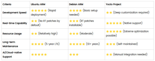
Comparison of Ubuntu, Debian, and Yocto for IIoT and Edge Computing
In industrial IoT (IIoT) and edge computing scenarios, Ubuntu, Debian, and Yocto Project each have unique advantages. Below is a detailed comparison and recommendations for these three systems:
1. Ubuntu (ARM)
Advantages
Ready-to-use: Provides official ARM images (e.g., Ubuntu Server 22.04 LTS) supporting hardware like Raspberry Pi and NVIDIA Jetson, requiring no complex configuration.
Cloud-native support: Built-in tools like MicroK8s, Docker, and Kubernetes, ideal for edge-cloud collaboration.
Long-term support (LTS): 5 years of security updates, meeting industrial stability requirements.
Rich software ecosystem: Access to AI/ML tools (e.g., TensorFlow Lite) and databases (e.g., PostgreSQL ARM-optimized) via APT and Snap Store.
Use Cases
Rapid prototyping: Quick deployment of Python/Node.js applications on edge gateways.
AI edge inference: Running computer vision models (e.g., ROS 2 + Ubuntu) on Jetson devices.
Lightweight K8s clusters: Edge nodes managed by MicroK8s.
Limitations
Higher resource usage (minimum ~512MB RAM), unsuitable for ultra-low-power devices.
2. Debian (ARM)
Advantages
Exceptional stability: Packages undergo rigorous testing, ideal for 24/7 industrial operation.
Lightweight: Minimal installation requires only 128MB RAM; GUI-free versions available.
Long-term support: Up to 10+ years of security updates via Debian LTS (with commercial support).
Hardware compatibility: Supports older or niche ARM chips (e.g., TI Sitara series).
Use Cases
Industrial controllers: PLCs, HMIs, and other devices requiring deterministic responses.
Network edge devices: Firewalls, protocol gateways (e.g., Modbus-to-MQTT).
Critical systems (medical/transport): Compliance with IEC 62304/DO-178C certifications.
Limitations
Older software versions (e.g., default GCC version); newer features require backports.
3. Yocto Project
Advantages
Full customization: Tailor everything from kernel to user space, generating minimal images (<50MB possible).
Real-time extensions: Supports Xenomai/Preempt-RT patches for μs-level latency.
Cross-platform portability: Single recipe set adapts to multiple hardware platforms (e.g., NXP i.MX6 → i.MX8).
Security design: Built-in industrial-grade features like SELinux and dm-verity.
Use Cases
Custom industrial devices: Requires specific kernel configurations or proprietary drivers (e.g., CAN-FD bus support).
High real-time systems: Robotic motion control, CNC machines.
Resource-constrained terminals: Sensor nodes running lightweight stacks (e.g., Zephyr+FreeRTOS hybrid deployment).
Limitations
Steep learning curve (BitBake syntax required); longer development cycles.
4. Comparison Summary
5. Selection Recommendations
Choose Ubuntu ARM: For rapid deployment of edge AI applications (e.g., vision detection on Jetson) or deep integration with public clouds (e.g., AWS IoT Greengrass).
Choose Debian ARM: For mission-critical industrial equipment (e.g., substation monitoring) where stability outweighs feature novelty.
Choose Yocto Project: For custom hardware development (e.g., proprietary industrial boards) or strict real-time/safety certification (e.g., ISO 13849) requirements.
6. Hybrid Architecture Example
Smart factory edge node:
Real-time control layer: RTOS built with Yocto (controlling robotic arms)
Data processing layer: Debian running OPC UA servers
Cloud connectivity layer: Ubuntu Server managing K8s edge clusters
Combining these systems based on specific needs can maximize the efficiency of IIoT edge computing.
0 notes
Text
AI in Precision Medicine Market: Impact on Personalized Healthcare Solutions

Executive Summary
The global AI in Precision Medicine Market is entering a period of explosive growth, projected to surge from USD 1.68 billion in 2022 to USD 17.15 billion by 2031, at a robust CAGR of 26.4%. This transformation is driven by AI’s unparalleled capability to unlock complex datasets and deliver individualized healthcare solutions. Stakeholders across the healthcare continuum—ranging from diagnostics and drug discovery to predictive analytics—are actively deploying AI to optimize clinical outcomes, reduce time-to-market, and enhance patient engagement.
Request Sample Report PDF (including TOC, Graphs & Tables): https://www.statsandresearch.com/request-sample/40461-global-artificial-intelligence-in-precision-medicine-market
AI in Precision Medicine Market Size Forecast and Historical Trajectory (2019–2031)
From 2019 to 2023, AI integration in precision medicine transitioned from exploratory pilot programs to full-scale implementations. Post-COVID-19 and amidst geopolitical disruptions, demand has accelerated due to the urgent need for scalable, data-driven healthcare systems.
AI in Precision Medicine Market Value Evolution
2019–2022: AI in precision medicine marketmatures beyond proof-of-concept stage
2023: Baseline year, consolidating AI workflows into clinical settings
2024–2031: Period of exponential expansion led by technological convergence and regulatory adaptability
Get up to 30%-40% Discount: https://www.statsandresearch.com/check-discount/40461-global-artificial-intelligence-in-precision-medicine-market
AI in Precision Medicine Market Regional Analysis: Strategic Opportunities by Geography
North America
Dominates the market with advanced infrastructure, massive healthcare data repositories, and innovation from leading tech firms. The U.S. leads due to its AI R&D funding and widespread adoption by pharma giants.
Asia-Pacific
High growth potential driven by government-backed AI initiatives, expanding genomics projects (notably in China, India, and Japan), and rising chronic disease burden.
Europe
Robust investment in digital health innovation through initiatives like Horizon Europe, alongside stringent but progressive regulatory frameworks supporting ethical AI.
Middle East & Africa and South America
Emerging markets demonstrating increased AI deployment in diagnostic imaging and telemedicine, particularly in Brazil, UAE, and South Africa.
Technology Landscape: Key Innovations Fueling Growth
Machine Learning (ML)
Automates complex pattern recognition in genomic and clinical datasets, enabling early disease detection and treatment customization.
Subcategories:
Supervised Learning: Critical in classification tasks (e.g., tumor detection)
Unsupervised Learning: Facilitates biomarker discovery through clustering and anomaly detection
Reinforcement Learning: Optimizes clinical decision-making pathways over time
Natural Language Processing (NLP)
Unlocks unstructured clinical text, such as physician notes and EHRs, offering rich insights into patient journeys and comorbidities.
Deep Learning
Drives breakthroughs in imaging diagnostics, enabling radiology systems to surpass human-level accuracy in interpreting scans.
Component Breakdown: Infrastructure Backbone
Hardware
Includes high-performance computing (HPC) units, GPUs (from firms like NVIDIA), and AI chips customized for biomedical modeling.
Software
Specialized AI platforms and SaaS tools for genomics, imaging, and therapeutic analytics—examples include Google DeepMind's health division and IBM Watson Health.
Services
Critical layer ensuring seamless integration, including cloud migration, AI model customization, and regulatory compliance consulting.
Application Spectrum: Where AI Delivers Value
Diagnostics
AI accelerates image interpretation (e.g., CT, MRI), molecular diagnostics, and genomic profiling—reducing diagnostic latency and errors.
Drug Discovery
Reduces R&D timelines through predictive modeling, compound screening, and virtual trials. Companies like Sanofi and AstraZeneca are leveraging AI to discover and validate drug targets faster.
Treatment Personalization
Analyzes multi-omic data to tailor therapies for oncology, rare diseases, and chronic conditions. Enables stratification of patient populations for maximum efficacy.
Predictive Analytics
Forecasts disease progression, relapse probabilities, and treatment responses. Integral for preventive healthcare models and value-based care frameworks.
End-Use Verticals: Sector-Wide Integration
Healthcare Providers
Deploy AI-powered clinical decision support systems (CDSS), enhance diagnostics, and personalize patient care at scale.
Research Institutions
Utilize AI for hypothesis generation, data mining of biological networks, and optimization of lab workflows.
Pharmaceutical Companies
Leverage AI in target identification, lead optimization, and clinical trial management. Notable case studies include the use of AI to repurpose drugs during the COVID-19 pandemic.
Competitive Landscape: Key AI in Precision Medicine Market Players
Major corporations and emerging disruptors are intensifying innovation in this space:
BioXcel Therapeutics: AI-driven neuroscience drug development
Sanofi: Partnerships for automated trial design
NVIDIA Corp.: GPUs tailored for health AI workloads
Alphabet Inc.: Pioneers in health-focused AI through subsidiaries like DeepMind and Verily
IBM Watson Health: Offers NLP-driven clinical insights
Microsoft & Intel: Providing cloud infrastructure and edge AI devices
AstraZeneca plc: AI-based compound screening
GE HealthCare: Imaging AI platforms integrated into radiology suites
Enlitic, Inc.: Focused on diagnostic radiology augmentation
Strategic Outlook: Key Growth Catalysts
Convergence of Genomics and AI Enhances resolution in patient stratification and therapeutic targeting.
Adoption of Digital Biomarkers Facilitates continuous patient monitoring and real-time data feeds.
Expansion of Regulatory Sandboxes Allows safe experimentation of AI models before full-scale deployment.
Data Interoperability Standards Enables seamless data integration across platforms and regions.
AI in Precision Medicine Market Challenges and Risk Factors
Data Privacy and Security: Rising scrutiny under regulations like GDPR and HIPAA
Algorithmic Bias: Necessitates fairness audits and representative training datasets
Integration Complexity: Legacy systems in healthcare pose interoperability barriers
Skill Gap: Shortage of domain-specific AI professionals hampers adoption
Purchase Exclusive Report: https://www.statsandresearch.com/enquire-before/40461-global-artificial-intelligence-in-precision-medicine-market
Conclusion
The AI in Precision Medicine market is on a trajectory of unprecedented transformation. With a projected 26.4% CAGR and an expanding range of clinical and commercial applications, this sector stands at the forefront of next-generation healthcare. Strategic investments, technological innovation, and collaborative ecosystems will dictate future market leadership.
To capture this growth, stakeholders must prioritize data infrastructure, model explainability, and cross-disciplinary collaboration. The next decade will not merely witness AI adoption—it will redefine the very fabric of personalized medicine.
Our Services:
On-Demand Reports: https://www.statsandresearch.com/on-demand-reports
Subscription Plans: https://www.statsandresearch.com/subscription-plans
Consulting Services: https://www.statsandresearch.com/consulting-services
ESG Solutions: https://www.statsandresearch.com/esg-solutions
Contact Us:
Stats and Research
Email: [email protected]
Phone: +91 8530698844
Website: https://www.statsandresearch.com
0 notes
Text
Evolution of Data Centers in the Age of AI and Machine Learning

As artificial intelligence (AI) and machine learning (ML) continue to revolutionize industries, data centers are undergoing significant transformations to meet the evolving demands of these technologies. This article explores the evolution of data centers from traditional models to advanced infrastructures tailored for AI and ML workloads.
Key considerations such as architectural flexibility, the role of specialized hardware, and the need for innovative cooling and data management solutions will be discussed. Additionally, we will delve into emerging trends like edge computing and quantum computing, which are shaping the future landscape of data centers in the age of AI and ML. To effectively manage these transformations, CCIE Data Center Training provides professionals with the expertise needed to navigate the complexities of modern data center environments.
Historical Overview: From Traditional to Modern Data Centers
Traditional Data Centers: Originally, data centers were primarily built on physical infrastructure with dedicated servers, network hardware, and storage systems. They focused on high reliability and uptime but were often inflexible and resource-intensive.
Emergence of Virtualization: The advent of virtualization technology allowed for more efficient resource utilization, leading to the rise of virtual machines (VMs) that could run multiple operating systems on a single physical server.
Cloud Computing Era: The introduction of cloud computing transformed data centers into scalable and flexible environments. This shift allowed organizations to leverage resources on demand, reducing capital expenditures and improving operational efficiency.
Modern Data Centers: Today's data centers are highly automated, utilizing software-defined networking (SDN) and storage (SDS) to enhance flexibility and reduce management complexity. They are designed to support various workloads, including artificial intelligence (AI) and machine learning (ML).
Key AI/ML Infrastructure Demands on Data Centers
High-Performance Computing (HPC): AI and ML require substantial computing power, necessitating infrastructures that can handle intensive workloads.
Scalability: The ability to quickly scale resources to accommodate fluctuating demands is critical for AI applications.
Low Latency: Real-time data processing is essential for AI applications, requiring architectures optimized for minimal latency.
Role of GPUs, TPUs, and Specialized Hardware in AI Data Centers
Graphics Processing Units (GPUs): GPUs are crucial for training AI models due to their ability to perform parallel processing, making them significantly faster than traditional CPUs for certain tasks.
Tensor Processing Units (TPUs): Developed by Google, TPUs are specialized hardware designed specifically for accelerating ML workloads, particularly for neural network models.
Custom AI Hardware: As AI continues to evolve, data centers are increasingly adopting custom chips and accelerators tailored for specific AI workloads, further enhancing performance.
Data Center Architecture for AI Workloads
Distributed Computing: AI workloads often require distributed architectures that can manage large datasets across multiple nodes.
Microservices: Adopting a microservices architecture allows for greater flexibility and faster deployment of AI applications.
Hybrid Architecture: Many organizations are employing hybrid architectures, combining on-premises data centers with public cloud resources to optimize performance and cost.
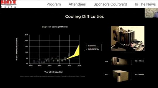
Cooling Solutions for High-Performance AI Data Centers
Advanced Cooling Techniques: Traditional air cooling is often inadequate for high-performance AI data centers. Innovative cooling solutions, such as liquid cooling and immersion cooling, are being utilized to manage the heat generated by dense compute clusters.
Energy Efficiency: Implementing energy-efficient cooling solutions not only reduces operational costs but also aligns with sustainability goals.
Data Management and Storage Requirements for AI/ML
Data Lakes: AI applications require large volumes of data, necessitating robust data management strategies, such as data lakes that support unstructured data storage.
Real-time Data Processing: The ability to ingest and process data in real-time is crucial for many AI applications, requiring optimized storage solutions that provide quick access to data.
The Role of Edge Computing in AI-Powered Data Centers
Edge Computing Overview: Edge computing involves processing data closer to the source rather than relying solely on centralized data centers. This is particularly important for IoT applications where latency is a concern.
AI at the Edge: Integrating AI capabilities at the edge allows for real-time analytics and decision-making, enhancing operational efficiencies and reducing bandwidth usage.
Security Challenges and Solutions for AI-Driven Data Centers
Increased Attack Surface: The complexity of AI-driven data centers creates more potential vulnerabilities, necessitating robust security measures.
AI in Cybersecurity: Leveraging AI for threat detection and response can enhance security postures, enabling quicker identification of anomalies and potential breaches.
Automation and Orchestration in AI-Enabled Data Centers
Role of Automation: Automation is critical for managing the complexities of AI workloads, enabling efficient resource allocation and scaling.
Orchestration Tools: Utilizing orchestration platforms helps in managing hybrid environments and optimizing workload distribution across different infrastructures.
Environmental and Energy Implications of AI in Data Centers
Energy Consumption: AI workloads can significantly increase energy consumption in data centers, leading to heightened operational costs and environmental concerns.
Sustainable Practices: Implementing sustainable practices, such as using renewable energy sources and improving energy efficiency, can mitigate the environmental impact of data centers.
Future Trends: Quantum Computing and AI Data Centers
Quantum Computing Potential: Quantum computing holds the potential to revolutionize AI by solving complex problems much faster than classical computers.
Integration of Quantum and AI: As quantum technology matures, the integration of quantum computing into AI data centers could enable unprecedented advancements in AI capabilities.
Impact of AI-Driven Data Centers on Industry Sectors
Healthcare: AI-driven data centers enhance data analysis for better patient outcomes and personalized medicine.
Finance: AI applications in data centers support real-time fraud detection and algorithmic trading.
Manufacturing: Automation and predictive analytics facilitated by AI in data centers optimize supply chain management and operational efficiency.
Conclusion:
In conclusion, the evolution of data centers in the age of AI and machine learning marks a significant transformation in how organizations manage and process data. From enhanced infrastructure demands and the integration of specialized hardware to innovative cooling solutions and energy-efficient practices, these advancements are reshaping the landscape of data management.
As industries increasingly rely on AI-driven capabilities, data centers must adapt to meet emerging challenges while optimizing for performance and sustainability.For professionals looking to excel in this evolving environment, obtaining certifications like CCIE Data Center can provide the necessary skills and knowledge to navigate these complexities. Embracing these changes will empower organizations to harness the full potential of AI, driving innovation and efficiency across various sectors.
#CCIE Data Center Training#CCIE Data Center#CCIE Data Center Course#CCIE Data Center Certification#CCIE Data Center Training in Bangalore
0 notes
Text
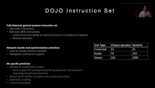
Optical I/O Shines Intel’s OCI Chiplet Powers Next-Decade AI

First Integrated Optical I/O Chiplet
With integrated photonics technology, Intel Corporation has made significant progress towards high-speed data transmission. The first-ever fully integrated optical computing interconnect (OCI) chiplet, co-packaged with an Intel CPU and executing real data, was showcased by Intel’s Integrated Photonics Solutions (IPS) Group at the Optical Fibre Communication Conference (OFC) 2024. This chiplet is the most sophisticated in the industry. By enabling co-packaged optical input/output (I/O) in developing AI infrastructure for data centres and high performance computing (HPC) applications, Intel’s OCI chiplet marks a significant advancement in high-bandwidth connection.
What It Does
This is the first OCI chiplet, intended to meet the increasing demands of AI infrastructure for greater bandwidth, lower power consumption, and longer reach. It can support 64 channels of 32 gigabits per second (Gbps) data transmission in each direction on up to 100 metres of fibre optics. It makes it possible for CPU/GPU cluster connectivity to grow in the future and for innovative compute designs like resource disaggregation and coherent memory extension.
Why It Matters
Large language models (LLM) and generative AI are two recent advancements that are speeding up the global deployment of AI-based applications. Machine learning (ML) models that are larger and more effective will be essential in meeting the new demands of workloads involving AI acceleration. Future AI computing platforms will need to be scaled, which will require exponential expansion in I/O bandwidth and longer reach to support larger CPU/GPU/IPU clusters and architectures with more effective resource utilisation, like memory pooling and xPU disaggregation.
High bandwidth density and low power consumption are supported via electrical I/O, or copper trace connectivity, although its reach is limited to one metre or less. When employed in data centres and early AI clusters, pluggable optical transceiver modules can expand reach at power and cost levels that are unsustainable for the scalability demands of AI workloads. AI/ML infrastructure scalability calls for co-packaged xPU optical I/O that can enable greater bandwidths with better power efficiency, longer reach, and low latency.
Electrical I/O
To use an analogy, switching from horse-drawn carriages, which had a limited capacity and range, to cars and trucks, which can transport much bigger amounts of products over much longer distances, is analogous to replacing electrical I/O with optical I/O in CPUs and GPUs to convey data. Optical I/O solutions such as Intel’s OCI chiplet could offer this kind of enhanced performance and energy efficiency to AI scalability.
How It Works
The fully integrated OCI chiplet combines an electrical integrated circuit (IC) with a silicon photonics integrated circuit (PIC), which incorporates on-chip lasers and optical amplifiers, by utilising Intel’s field-proven silicon photonics technology. Although the OCI chiplet showcased at OFC was co-packaged with an Intel CPU, it can be combined with different system-on-chips (SoCs), GPUs, IPUs, and next-generation CPUs.
This initial OCI version is compatible with PCIe Gen5 and provides bidirectional data transmission rates of up to 4 terabits per second (Tbps). A transmitter (Tx) and receiver (Rx) connection between two CPU platforms via a single-mode fibre (SMF) patch cord is shown in the live optical link demonstration. The demonstration shows the Tx optical spectrum with 8 wavelengths at 200 gigahertz (GHz) spacing on a single fibre, along with a 32 Gbps Tx eye diagram demonstrating strong signal quality. The CPUs generated and tested the optical Bit Error Rate (BER).
The current chiplet uses eight fibre pairs, each carrying eight dense wavelength division multiplexing (DWDM) wavelengths, to provide 64 channels of 32 Gbps data in each direction up to 100 metres (though actual implementations may be limited to tens of metres due to time-of-flight latency). In addition to being incredibly energy-efficient, the co-packaged solution uses only 5 pico-Joules (pJ) per bit, as opposed to around 15 pJ/bit for pluggable optical transceiver modules. AI’s unsustainable power requirements may be addressed with the help of this level of hyper-efficiency, which is essential for data centres and high-performance computing settings.
Concerning Intel’s Preeminence in Silicon Photonics
With over 25 years of in-house research from Intel Labs, the company that invented integrated photonics, Intel is a market leader in silicon photonics. The first business to create and supply industry-leading dependability silicon photonics-based connectivity solutions in large quantities to major cloud service providers was Intel.
The primary point of differentiation for Intel is their unmatched integration of direct and hybrid laser-on-wafer technologies, which result in reduced costs and increased reliability. Intel is able to preserve efficiency while delivering higher performance thanks to this innovative method. With over 8 million PICs and over 32 million integrated on-chip lasers shipped, Intel’s reliable, high-volume platform has a laser failures-in-time (FIT) rate of less than 0.1, which is a commonly used reliability metric that shows failure rates and the frequency of failures.
For use in 100, 200, and 400 Gbps applications, these PICs were installed in big data centre networks at prominent hyperscale cloud service providers in the form of pluggable transceiver modules. In development are next generation 200G/lane PICs to handle 800 Gbps and 1.6 Tbps applications that are only starting to gain traction.
Additionally, Intel is introducing a new fab process node for silicon photonics that offers significantly better economics, higher density, better coupling, and state-of-the-art (SOA) device performance. Intel keeps improving SOA performance, cost (more than 40% reduction in die size), power (more than 15% reduction), and on-chip laser performance.
What’s Next
This OCI chiplet from Intel is a prototype. Intel is collaborating with a small number of clients to co-package OCI as an optical I/O solution with their SoCs.
The OCI chiplet from Intel is a significant advancement in high-speed data transfer. Intel continues to be at the forefront of innovation and is influencing the future of connectivity as the AI infrastructure landscape changes.
Read more on govindhtech.com
#Opticali#Ointels#oci#Decadeai#Chiplet#cpu#PowersNext#Machinelearning#ml#Largelanguagemodels#llm#gen5#SiliconPhotonics#technology#technews#news#govindhtech
1 note
·
View note
Text
I have this Ars Technica article pinned in my clipboard now because of how often I've had to cite it as a sort of accessible primer to why the oft-cited numbers on AI power consumption are, to put it kindly, very very wrong. The salient points of the article are that the power consumption of AI is, in the grand scheme of datacenter power consumption, a statistically insignificant blip. While the power consumption of datacenters *has* been growing, it's been doing so steadily for the past twelve years, which AI had nothing to do with. Also, to paraphrase my past self:
While it might be easy to look at the current massive AI hypetrain and all the associated marketing and think that Silicon Valley is going cuckoo bananas over this stuff long term planning be damned, the fact is that at the end of the day it's engineers and IT people signing off on the acquisitions, and they are extremely cautious, to a fault some would argue, and none of them wanna be saddled with half a billion dollars worth of space heaters once they no longer need to train more massive models (inference is an evolving landscape and I could write a whole separate post about that topic).
Fundamentally, AI processors like the H100 and AMD's Instinct MI300 line are a hedged bet from all sides. The manufacturers don't wanna waste precious wafer allotment on stock they might not be able to clear in a year's time, and the customers don't wanna buy something that ends up being a waste of sand in six months time once the hype machine runs out of steam. That's why these aren't actually dedicated AI coprocessors, they're just really really fucking good processors for any kind of highly parallel workload that requires a lot of floating point calculations and is sensitive to things like memory capacity, interconnect latencies, and a bunch of other stuff. And yeah, right now they're mainly being used for AI, and there's a lot of doom and gloom surrounding that because AI is, of course, ontologically evil (except when used in ways that read tastefully in a headline), and so their power consumption seems unreasonably high and planet-destroying. But those exact same GPUs, at that exact same power consumption, in those same datacenters, can and most likely *will* be used for things like fluid dynamics simulations, or protein folding for medical research, both of which by the way are usecases that AI would also be super useful in. In fact, they most likely currently are being used for those things! You can use them for it yourself! You can go and rent time on a compute cluster of those GPUs for anything you want from any of the major cloud service providers with trivial difficulty!
A lot of computer manufacturers are actually currently developing specific ML processors (these are being offered in things like the Microsoft copilot PCs and in the Intel sapphire processors) so reliance on GPUs for AI is already receding (these processors should theoretically also be more efficient for AI than GPUs are, reducing energy use).
Regarding this, yes! Every major CPU vendor (and I do mean every one, not just Intel and AMD but also MediaTek, Qualcomm, Rockchip,and more) are integrating dedicated AI inference accelerators into their new chips. These are called NPUs, or Neural Processing Units. Unlike GPUs, which are Graphics Processing Units (and just so happen to also be really good for anything else that's highly parallel, like AI), NPUs do just AI and nothing else whatsoever. And because of how computers work, this means that they are an order of magnitude more efficient in every way than their full-scale GPU cousins. They're cheaper to design, cheaper to manufacture, run far more efficiently, and absolutely sip power during operation. Heck, you can stick one in a laptop and not impact the battery life! Intel has kind of been at the forefront of these, bringing them to their Sapphire Rapids Xeon CPUs for servers and workstations to enable them to compete with AMD's higher core counts (with major South Korean online services provider Naver Corporation using these CPUs over Nvidia GPUs due to supply issues and price hikes), and being the first major vendor to bring NPUs to the consumer space with their Meteor Lake or first generation Core Ultra lineup (followed shortly by AMD and then Qualcomm). If you, like me, are a colossal giganerd and wanna know about the juicy inside scoop on how badly Microsoft has screwed the whole kit and caboodle and also a bunch of other cool stuff, Wendell from Level1Techs has a really great video going over all that stuff! It's a pretty great explainer on just why, despite the huge marketing push, AI for the consumer space (especially Copilot) has so far felt a little bit underwhelming and lacklustre, and if you've got the time it's definitely worth a watch!
I don't care about data scraping from ao3 (or tbh from anywhere) because it's fair use to take preexisting works and transform them (including by using them to train an LLM), which is the entire legal basis of how the OTW functions.
#sorry for the massive text wall and all the technobabble#and also the random tangents#I'm bad at making my writing accessible#it's hard to simplify these concepts down to the scale where most people could intuit them without basically writing a crash course#on current affairs in the tech world#I did try though#honest! I did!#I'm just not very good at it
3K notes
·
View notes
Text
The Future of AI is Here: Cerebras' WSE-2 is the largest computer chip ever built and the fastest AI processor on Earth
See on Scoop.it - Design, Science and Technology
Cluster-Scale Performance on a Single Large-Wafer Chip
Video is here
Programming a cluster to scale deep learning is painful. It typically requires dozens to hundreds of engineering hours and remains a practical barrier for many to realize the value of large-scale AI for their work. On a traditional GPU cluster, ML researchers – typically using a special version of their ML framework – must figure out how to distribute their model while still achieving some fraction of their convergence and performance target. They must navigate the complex hierarchy of individual processors’ memory capacity, bandwidth, interconnect topology, and synchronization; all while performing a myriad of hyper-parameter and tuning experiments along the way. What’s worse is that the resultant implementation is brittle to change, and this time only delays overall time to solution. With the WSE, there is no bottleneck. We give you a cluster-scale AI compute resource with the programming ease of a single desktop machine using stock TensorFlow or PyTorch. Spend your time in AI discovery, not cluster engineering.
Learn more
Designed for AI
Each core on the WSE is independently programmable and optimized for the tensor-based, sparse linear algebra operations that underpin neural network training and inference for deep learning, enabling it to deliver maximum performance, efficiency, and flexibility. The WSE-2 packs 850,000 of these cores onto a single processor. With that, and any data scientist can run state-of-the-art AI models and explore innovative algorithmic techniques at record speed and scale, without ever touching distributed scaling complexities.
1000x Memory Capacity and Bandwidth
Unlike traditional devices, in which the working cache memory is tiny, the WSE-2 takes 40GB of super-fast on-chip SRAM and spreads it evenly across the entire surface of the chip. This gives every core single-clock-cycle access to fast memory at extremely high bandwidth – 20 PB/s. This is 1,000x more capacity and 9,800x greater bandwidth than the leading GPU. This means no trade-off is required. You can run large, state-of-the art models and real-world datasets entirely on a single chip. Minimize wall clock training time and achieve real-time inference within latency budgets, even for large models and datasets.
220Pb/s
High Bandwidth - Low Latency
Deep learning requires massive communication bandwidth between the layers of a neural network. The WSE uses an innovative high bandwidth, low latency communication fabric that connects processing elements on the wafer at tremendous speed and power efficiency. Dataflow traffic patterns between cores and across the wafer are fully configurable in software. The WSE-2 on-wafer interconnect eliminates the communication slowdown and inefficiencies of connecting hundreds of small devices via wires and cables. It delivers an incredible 220 Pb/s processor-processor interconnect bandwidth. That’s more than 45,000x the bandwidth delivered between graphics processors.
Read the full article at: www.cerebras.net
0 notes
Photo
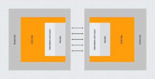
High Speed Chip-to-Chip Interface Protocol-Member of Interlaken Alliance-Interlaken IP Core-Chip-to-Chip and Die-to-Die Connectivity-AI/ML Chip Clusters
We offer Interlaken IP Subsystem, High-speed chip-to-chip interface protocol, Chip-to-Chip, Die-to-Die connectivity, and Forward Error Correction (FEC).
#high speed chip-to-chip interface protocol#Member of Interlaken Alliance#Interlaken IP Core#chip-to-chip and die-to-die connectivity#ai/ml chip clusters
0 notes
Text
Google and Tesla Will Compete With 10-100 Exaflop AI Clouds
In early 2022, Google revealed it is operating a full cluster of eight of these AI supercomputing pods in its Oklahoma data center. There is combined 9 exaflops of peak aggregate performance. Google believes this makes this ��the world’s largest publicly available ML hub in terms of cumulative computing power, while operating at 90% carbon-free energy.”
Google plans to buidl a dozen AI data centers.
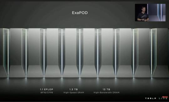
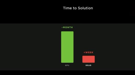
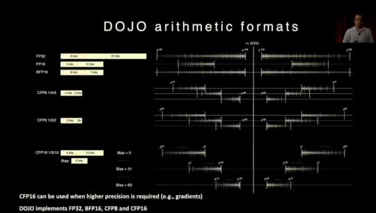
Tesla Announced AI Dojo Training at the Scale of Google AI Cloud

Each Tesla Dojo AI training tray consists of six training tiles. Tesla said each 135kg tray offers 54 petaflops (BF16/CFP8) and requires 100kW+ of power.
Each cabinet holds two trays and accompanying interface equipment. In Q1 2023, 10 cabinets will be connected into one ‘Exapod’ that will be the 1.1 exaflops (BF16/CFP8) Dojo system.
Tesla plans to install a total of seven ExaPods in Palo Alto, potentially offering 8.8 exaflops (BF16/CFP8). This will be competitive with the Google Oklahoma data center.
Musk said Tesla may offer Dojo to companies as a AI Cloud service.
Tesla is building next generation Dojo chips and tiles that will provide another 4X in performance.


Brian Wang is a Futurist Thought Leader and a popular Science blogger with 1 million readers per month. His blog Nextbigfuture.com is ranked #1 Science News Blog. It covers many disruptive technology and trends including Space, Robotics, Artificial Intelligence, Medicine, Anti-aging Biotechnology, and Nanotechnology.
Known for identifying cutting edge technologies, he is currently a Co-Founder of a startup and fundraiser for high potential early-stage companies. He is the Head of Research for Allocations for deep technology investments and an Angel Investor at Space Angels.
A frequent speaker at corporations, he has been a TEDx speaker, a Singularity University speaker and guest at numerous interviews for radio and podcasts. He is open to public speaking and advising engagements.
0 notes
Text
GigaIO Fabrex™: The Highest Performance, Lowest Latency Rack-Scale Network on the Planet
Imagine this…
You just spent a lot on a rack of servers and multiple GPUs to solve your computational problems.
You don’t know it yet, but your GPUs are mostly left untouched even with finely tuned models and servers, so you end up wasting space, energy, and well. your power bills.
GigaIO™ solves this problem with FabreX – the highest performance, lowest latency rack-scale network you can get.
With FabreX, you can now increase utilisation and eliminate over provisioning of resources, which helps reduce cooling expenses. On top of that, you’re also able to save space with fewer power-consuming servers and accelerators for the exact same performance.
You must be wondering…
What is GigaIO™?
GigaIO™ provides Composable Disaggregated Infrastructure solutions, which comes in both hardware and software.
The hardware consists of:
· FabreX Top of Rack (TOR) Switch
· FabreX PCIe Gen4 Adapter
GigaIO™ FabreX™ Network Adapter Card enables non-blocking low-latency PCIe Gen4 which gives AI/ML, HPC, and Data Analytics users the flexibility to create exactly the system they need for optimised performance and reduced total cost of ownership.
· Accelerator Pooling Appliance
The GigaIO™ Gen4 Accelerator Pooling Appliance is the industry’s highest performing PCIe accelerator appliance fully supporting PCIe Gen4 with up to 1Tb/sec bandwidth into and out of the box. Support up to 8 double-width PCIe Gen 4.0 x16 accelerator cards with up to 300W delivered to every slot; and 2 PCIe Gen 4.0 x16 low-profile slots.
Besides GPUs, it also supports FPGAs, IPUs, DPUs, thin-NVMe-servers and specialty AI chips.
The software offered:
· FabreX Software
A Linux-based, resource-efficient software layers engine that drives the performance and dynamic composability of GigaIO’s Software-Defined HardwareTM (SDH).
It integrates with Bright Cluster Manager that supports popular HPC workload schedulers such as SLURM, PBS Pro & OpenPBS, LSF, Altair Grid Engine, Kubernetes.
For infrastructure integration it supports Bright Cluster Manager VMware vSphere integration and Supermicro SuperCloud Composer.
What solution does GigaIO™ offer?
Through an all-new architecture, GigaIO™ offers a hyper-performance network that enables a unified, software-driven composable infrastructure.
In other words, GigaIO™ allows CPU, GPU Accelerator, and NVMe drives that are installed in any server or in an external chassis to be shared among multiple servers. As a result, you no longer have to detach drives from the initial physical server to be reinstalled in another server.
Namely, GigaIO™ FabreX enables you to connect 32 GPUs with only 1 server. Not only does this reduce the total cost of ownership (TCO), the infrastructure management is simpler too. Additionally, the low latency interconnection also provides superior performance.
What do we mean by reducing TCO?
By implementing GigaIO solution, you can:
1. Spend less to get the same performance and capacity as compared to other solutions.
2. Get ROI (Return on Investment) faster because it allows the customer to do exactly the same things but with lower cost. The GigaIO solution enables you to achieve ROI in half the standard time.
3. Do more things with GigaIO, for example, GigaIO supports orchestration of ANY Compute, Acceleration (CPUs, GPUs, FPGAs, ASICs), Storage, Memory (3D-XPoint) or Networking resource for any workload using an Enterprise-Class, Easy-To-Use and Open Standards high-performance network.
How does it work?
FabreX is the only fabric which enables complete disaggregation and composition of all the resources in your server rack. Besides composing resources to servers, FabreX can also compose your servers over PCIe (and CXL in the future), without the cost, complexity and latency hit from having to switch to Ethernet or InfiniBand within the rack.
With any workload that needs more than one server and more resources (storage, GPUs, FPGAs, etc.), FabreX is exactly what you need. Typical workloads centre around the use of GPU and FPGA accelerators, including AI/ML/DL, visualisation, High Performance Computing and Data Analytics.
For more use cases visit our solutions page.
In Robust HPC, we use GigaIO’s FabreX universal dynamic fabric to enable true rack-scale computing, breaking the limits of the server box to enable the entire rack the unit of compute.
Resources such as GPU, FGPAs, ASICs and NVMe are connected via low latency FabreX switches (less than 110ns with non-blocking ports) and can be configured in various ways depending on your needs.
Long story short, you get the flexibility and agility of the cloud, but with the security and cost control of your own on-prem infrastructure.
Get in touch with Robust HPC – an authorised reseller of GigaIO in Southeast Asia, to know more about how organisations use GigaIO and find the right use case to address your computing needs.
Article Source: https://www.robusthpc.com/gigaio-fabrex/
0 notes
Text
Comparison of Ubuntu, Debian, and Yocto for IIoT and Edge Computing
In industrial IoT (IIoT) and edge computing scenarios, Ubuntu, Debian, and Yocto Project each have unique advantages. Below is a detailed comparison and recommendations for these three systems:
1. Ubuntu (ARM)
Advantages
Ready-to-use: Provides official ARM images (e.g., Ubuntu Server 22.04 LTS) supporting hardware like Raspberry Pi and NVIDIA Jetson, requiring no complex configuration.
Cloud-native support: Built-in tools like MicroK8s, Docker, and Kubernetes, ideal for edge-cloud collaboration.
Long-term support (LTS): 5 years of security updates, meeting industrial stability requirements.
Rich software ecosystem: Access to AI/ML tools (e.g., TensorFlow Lite) and databases (e.g., PostgreSQL ARM-optimized) via APT and Snap Store.
Use Cases
Rapid prototyping: Quick deployment of Python/Node.js applications on edge gateways.
AI edge inference: Running computer vision models (e.g., ROS 2 + Ubuntu) on Jetson devices.
Lightweight K8s clusters: Edge nodes managed by MicroK8s.
Limitations
Higher resource usage (minimum ~512MB RAM), unsuitable for ultra-low-power devices.
2. Debian (ARM)
Advantages
Exceptional stability: Packages undergo rigorous testing, ideal for 24/7 industrial operation.
Lightweight: Minimal installation requires only 128MB RAM; GUI-free versions available.
Long-term support: Up to 10+ years of security updates via Debian LTS (with commercial support).
Hardware compatibility: Supports older or niche ARM chips (e.g., TI Sitara series).
Use Cases
Industrial controllers: PLCs, HMIs, and other devices requiring deterministic responses.
Network edge devices: Firewalls, protocol gateways (e.g., Modbus-to-MQTT).
Critical systems (medical/transport): Compliance with IEC 62304/DO-178C certifications.
Limitations
Older software versions (e.g., default GCC version); newer features require backports.
3. Yocto Project
Advantages
Full customization: Tailor everything from kernel to user space, generating minimal images (<50MB possible).
Real-time extensions: Supports Xenomai/Preempt-RT patches for μs-level latency.
Cross-platform portability: Single recipe set adapts to multiple hardware platforms (e.g., NXP i.MX6 → i.MX8).
Security design: Built-in industrial-grade features like SELinux and dm-verity.
Use Cases
Custom industrial devices: Requires specific kernel configurations or proprietary drivers (e.g., CAN-FD bus support).
High real-time systems: Robotic motion control, CNC machines.
Resource-constrained terminals: Sensor nodes running lightweight stacks (e.g., Zephyr+FreeRTOS hybrid deployment).
Limitations
Steep learning curve (BitBake syntax required); longer development cycles.
4. Comparison Summary

5. Selection Recommendations
Choose Ubuntu ARM: For rapid deployment of edge AI applications (e.g., vision detection on Jetson) or deep integration with public clouds (e.g., AWS IoT Greengrass).
Choose Debian ARM: For mission-critical industrial equipment (e.g., substation monitoring) where stability outweighs feature novelty.
Choose Yocto Project: For custom hardware development (e.g., proprietary industrial boards) or strict real-time/safety certification (e.g., ISO 13849) requirements.
6. Hybrid Architecture Example
Smart factory edge node:
Real-time control layer: RTOS built with Yocto (controlling robotic arms)
Data processing layer: Debian running OPC UA servers
Cloud connectivity layer: Ubuntu Server managing K8s edge clusters
Combining these systems based on specific needs can maximize the efficiency of IIoT edge computing.
0 notes
Text
Top 9 Popular Python Libraries for AI-ML Applications
AI-ML is one the most code-dense applications in computer science. Thanks to the simpler syntaxes and versatility of Python, it intrigued a vibrant community of coders to develop and contribute algorithms that suit Machine Learning (ML) operations. The norm about ‘get more and code less’ has ranked Python to the top. Plus Python in itself is highly intuitive, as a result, it’s a faster alternative for ML engineers to make smarter predictive algorithms.
All the years of python development have accumulated a fair amount of algorithms that are ready to use. The extensive math work from the coders is curated as numerical libraries which reduce the burden to code and are converted to functional tool-kits that can be applied to varied chapters of ML. The standard libraries include a number of internet protocols, string operations, web service tools, and operating system interfaces that are scripted. Another advantage to Python is loyalty-free use even for commercial purposes and OSI services which helps it to take part in the larger part of a larger part of the community-driven by similar sentiments.

Without further adieu let us take a look at the python libraries that we have listed today.
Numpy - One of the most popular libraries among python users which consists of a large multi-dimensional array and matrix processing algorithms, making it a rich source of high-level mathematical functions. Operations like linear algebra, Fourier transforms, random number calculations, and probability functions can be performed easily by using Numpy solutions. Numpy harbors popular ML libraries that allow scientific computations and with the growing volume of the scripts, the libraries forked into sub-libraries like scipy, sci-kit learn, and others. Plus it is an essential component in the growing Python visualization landscape, enabling researchers to visualize datasets better than native python itself.
Scikit-learn- previously known as scikits.learn or Sklearn, which has a wide range of ML algorithms and simple & efficient tools for predictive data analysis. It hosts an array of features used for various classification, to perform regression analysis, clustering, multi-dimensional reduction in ML, and pre-processing of data for supervised and unsupervised learning. This spectrum of tools are built based on NumPy, SciPy, and matplotlib and share open access to users and can be reused in a different context.
matplotlib - A plotting function library for Python which is extensively used for data visualization purposes. Unlike Pandas which is directly related to machine learning, it behaves as numerical mathematics extensions that enable 2D to 3D plotting and are used to provide object-oriented APIs. With the help of matplotlib, a programmer will be able to use general-purpose GUIs toolkits like Tkinter, wxPython, Qt, or GTK. Its Pylab interface closely resembles MATLAB, which branched as an intention of Scipy. In simpler terms, it’s an easy module for data visualization like histogram, error charts, bar charts.
TensorFlow- A computational framework extensively used for tensor modeling for ML applications. TensorFlow not only supports a variety of different toolkits for constructing models it also runs smoothly with Python and C++ APIs. It has a flexible architecture and can run computational platforms like CPUs, GPUs, and TPUs. TPU stands for Tensor processing unit, a hardware chip specifically built around TensorFlow for ML-AI applications. Plus it can train and run deep neural networks and widely used for deep learning research and applications.
Keras - Keras comes as default after TensorFlow as the library is built based on the toolkits Theano, Microsoft Cognitive, R, PlaidML and of course TensorFlow. Keras also can run efficiently on CPU and GPU, involving in operations like neural-network building, activation functions, and optimizers. Keras supports convolutional and recurrent neural networks and also has a bunch of features for images and text image editing to writing Deep Neural Network codes.
Pandas- Pandas is a popular Python library for data analysis. It is not directly related to Machine Learning. As we know that the dataset must be prepared before training - in this case, Pandas comes in handy as it was developed specifically for data extraction and preparation. It provides high-level data structures and a wide variety of tools for data analysis. It provides many inbuilt methods for groping, combining, and filtering data.
Scipy- A popular ML library enthus containing different modules for optimization, linear algebra, integration, and statistics. There is a difference between the SciPy library and the SciPy stack. The SciPy is one of the core packages that make up the SciPy stack. SciPy is also very useful for image manipulation.
Theano- python library that evaluates and optimizes mathematical expressions involving multi-dimensional arrays. It is achieved by optimizing the utilization of CPU and GPU and used for unit-testing and self-verification, diagnosis and detection of different types of errors. Theano is a very powerful library that has been used in large-scale computationally intensive scientific projects for a long time but is simple and approachable enough to be used by individuals for their own projects.
Pytorch- PyTorch is a popular open-source Machine Learning library for Python based on Torch, which is an open-source Machine Learning library that is implemented in C with a wrapper in Lua. It has an extensive choice of tools and libraries that support Computer Vision, Natural Language Processing(NLP), and many more ML programs. It allows developers to perform computations on Tensors with GPU acceleration and also helps in creating computational graphs.
Keeping the demand in mind about the growing enterprise application for AI, Miles Education is offering an array of PG certifications in AI-ML applications and sector focussed programs from IIT Roorkee and IIT Mandi in collaboration with Wiley. This course will walk you through deep AI processing and industry-specific tools to follow-though the entire AI lifecycle. Throughout the program, you can learn about modeling user-friendly APIs with tools like Python, Keras, Tensorflow, NLTK, NumPy, Scikit-learn, Pandas, Jupyter, and Matplotlib. Plus you will learn to 'Apply AI' in real-world scenarios under the guidance of the top industry experts organized by the Wiley Innovation Advisory Council, with a choice of programs from-
IIT Mandi & Wiley - PG Certification in Applied AI & ML
IIT Roorkee & Wiley - PG Certification in AI for BFSI
IIT Roorkee & Wiley - PG Certification in AI for Digital Businesses & E-Commerce
#ai#python#machine learning#ML#bfsi#digital#businessanalytics#tech#certification#artificial intelligence#tensorflow
0 notes
Text
Habana Labs launches its Gaudi AI training processor
Habana Labs, a Tel Aviv-based AI processor startup, today announced its Gaudi AI training processor, which promises to easily beat GPU-based systems by a factor of four. While the individual Gaudi chips beat GPUs in raw performance, it’s the company’s networking technology that gives it the extra boost to reach its full potential.
Gaudi will be available as a standard PCIe card that supports eight ports of 100Gb Ethernet, as well as a mezzanine card that is compliant with the relatively new Open Compute Project accelerator module specs. This card supports either the same ten 100GB Ethernet ports or 20 ports of 50Gb Ethernet. The company is also launching a system with eight of these mezzanine cards.
Last year, Habana Labs previously launched its Goya inferencing solution. With Gaudi, it now offers a complete solution for businesses that want to use its hardware over GPUs with chips from the likes of Nvidia. Thanks to its specialized hardware, Gaudi easily beats an Nvidia T4 accelerator on most standard benchmarks — all while using less power.
“The CPU and GPU architecture started from solving a very different problem than deep learning,” Habana CBO Eitan Medina told me. “The GPU, almost by accident, happened to be just better because it has a higher degree of parallelism. However, if you start from a clean sheet of paper and analyze what a neural network looks like, you can, if you put really smart people in the same room […] come up with a better architecture.” That’s what Habana did for its Goya processor and it is now taking what it learned from this to Gaudi.
For developers, the fact that Habana Labs supports all of the standard AI/ML frameworks, as well as the ONNX format, should make the switch from one processor to another pretty painless.
“Training AI models require exponentially higher compute every year, so it’s essential to address the urgent needs of the data center and cloud for radically improved productivity and scalability. With Gaudi’s innovative architecture, Habana delivers the industry’s highest performance while integrating standards-based Ethernet connectivity, enabling unlimited scale,” said David Dahan, CEO of Habana Labs. “Gaudi will disrupt the status quo of the AI Training processor landscape.”
As the company told me, the secret here isn’t just the processor itself but also how it connects to the rest of the system and other processors (using standard RDMA RoCE, if that’s something you really care about).
Habana Labs argues that scaling a GPU-based training system beyond 16 GPUs quickly hits a number of bottlenecks. For a number of larger models, that’s becoming a necessity, though. With Gaudi, that becomes simply a question of expanding the number of standard Ethernet networking switches so that you could easily scale to a system with 128 Gaudis.
“With its new products, Habana has quickly extended from inference into training, covering the full range of neural-network functions,” said Linley Gwennap, principal analyst of The Linley Group. “Gaudi offers strong performance and industry-leading power efficiency among AI training accelerators. As the first AI processor to integrate 100G Ethernet links with RoCE support, it enables large clusters of accelerators built using industry-standard components.”
0 notes