#Defect detection in semiconductor wafers
Explore tagged Tumblr posts
Visit Tumblr Blog
Explore Tumblr blogs with no restrictions, modern design and the best experience.
Last Seen Tumblr Blogs


Fun Fact
Tumblr’s website traffic is steadily declining.
Text
Machine learning applications in semiconductor manufacturing
Machine Learning Applications in Semiconductor Manufacturing: Revolutionizing the Industry
The semiconductor industry is the backbone of modern technology, powering everything from smartphones and computers to autonomous vehicles and IoT devices. As the demand for faster, smaller, and more efficient chips grows, semiconductor manufacturers face increasing challenges in maintaining precision, reducing costs, and improving yields. Enter machine learning (ML)—a transformative technology that is revolutionizing semiconductor manufacturing. By leveraging ML, manufacturers can optimize processes, enhance quality control, and accelerate innovation. In this blog post, we’ll explore the key applications of machine learning in semiconductor manufacturing and how it is shaping the future of the industry.
Predictive Maintenance
Semiconductor manufacturing involves highly complex and expensive equipment, such as lithography machines and etchers. Unplanned downtime due to equipment failure can cost millions of dollars and disrupt production schedules. Machine learning enables predictive maintenance by analyzing sensor data from equipment to predict potential failures before they occur.
How It Works: ML algorithms process real-time data from sensors, such as temperature, vibration, and pressure, to identify patterns indicative of wear and tear. By predicting when a component is likely to fail, manufacturers can schedule maintenance proactively, minimizing downtime.
Impact: Predictive maintenance reduces equipment downtime, extends the lifespan of machinery, and lowers maintenance costs.
Defect Detection and Quality Control
Defects in semiconductor wafers can lead to significant yield losses. Traditional defect detection methods rely on manual inspection or rule-based systems, which are time-consuming and prone to errors. Machine learning, particularly computer vision, is transforming defect detection by automating and enhancing the process.
How It Works: ML models are trained on vast datasets of wafer images to identify defects such as scratches, particles, and pattern irregularities. Deep learning algorithms, such as convolutional neural networks (CNNs), excel at detecting even the smallest defects with high accuracy.
Impact: Automated defect detection improves yield rates, reduces waste, and ensures consistent product quality.
Process Optimization
Semiconductor manufacturing involves hundreds of intricate steps, each requiring precise control of parameters such as temperature, pressure, and chemical concentrations. Machine learning optimizes these processes by identifying the optimal settings for maximum efficiency and yield.
How It Works: ML algorithms analyze historical process data to identify correlations between input parameters and output quality. Techniques like reinforcement learning can dynamically adjust process parameters in real-time to achieve the desired outcomes.
Impact: Process optimization reduces material waste, improves yield, and enhances overall production efficiency.
Yield Prediction and Improvement
Yield—the percentage of functional chips produced from a wafer—is a critical metric in semiconductor manufacturing. Low yields can result from various factors, including process variations, equipment malfunctions, and environmental conditions. Machine learning helps predict and improve yields by analyzing complex datasets.
How It Works: ML models analyze data from multiple sources, including process parameters, equipment performance, and environmental conditions, to predict yield outcomes. By identifying the root causes of yield loss, manufacturers can implement targeted improvements.
Impact: Yield prediction enables proactive interventions, leading to higher productivity and profitability.
Supply Chain Optimization
The semiconductor supply chain is highly complex, involving multiple suppliers, manufacturers, and distributors. Delays or disruptions in the supply chain can have a cascading effect on production schedules. Machine learning optimizes supply chain operations by forecasting demand, managing inventory, and identifying potential bottlenecks.
How It Works: ML algorithms analyze historical sales data, market trends, and external factors (e.g., geopolitical events) to predict demand and optimize inventory levels. Predictive analytics also helps identify risks and mitigate disruptions.
Impact: Supply chain optimization reduces costs, minimizes delays, and ensures timely delivery of materials.
Advanced Process Control (APC)
Advanced Process Control (APC) is critical for maintaining consistency and precision in semiconductor manufacturing. Machine learning enhances APC by enabling real-time monitoring and control of manufacturing processes.
How It Works: ML models analyze real-time data from sensors and equipment to detect deviations from desired process parameters. They can automatically adjust settings to maintain optimal conditions, ensuring consistent product quality.
Impact: APC improves process stability, reduces variability, and enhances overall product quality.
Design Optimization
The design of semiconductor devices is becoming increasingly complex as manufacturers strive to pack more functionality into smaller chips. Machine learning accelerates the design process by optimizing chip layouts and predicting performance outcomes.
How It Works: ML algorithms analyze design data to identify patterns and optimize layouts for performance, power efficiency, and manufacturability. Generative design techniques can even create novel chip architectures that meet specific requirements.
Impact: Design optimization reduces time-to-market, lowers development costs, and enables the creation of more advanced chips.
Fault Diagnosis and Root Cause Analysis
When defects or failures occur, identifying the root cause can be challenging due to the complexity of semiconductor manufacturing processes. Machine learning simplifies fault diagnosis by analyzing vast amounts of data to pinpoint the source of problems.
How It Works: ML models analyze data from multiple stages of the manufacturing process to identify correlations between process parameters and defects. Techniques like decision trees and clustering help isolate the root cause of issues.
Impact: Faster fault diagnosis reduces downtime, improves yield, and enhances process reliability.
Energy Efficiency and Sustainability
Semiconductor manufacturing is energy-intensive, with significant environmental impacts. Machine learning helps reduce energy consumption and improve sustainability by optimizing resource usage.
How It Works: ML algorithms analyze energy consumption data to identify inefficiencies and recommend energy-saving measures. For example, they can optimize the operation of HVAC systems and reduce idle time for equipment.
Impact: Energy optimization lowers operational costs and reduces the environmental footprint of semiconductor manufacturing.
Accelerating Research and Development
The semiconductor industry is driven by continuous innovation, with new materials, processes, and technologies being developed regularly. Machine learning accelerates R&D by analyzing experimental data and predicting outcomes.
How It Works: ML models analyze data from experiments to identify promising materials, processes, or designs. They can also simulate the performance of new technologies, reducing the need for physical prototypes.
Impact: Faster R&D cycles enable manufacturers to bring cutting-edge technologies to market more quickly.
Challenges and Future Directions
While machine learning offers immense potential for semiconductor manufacturing, there are challenges to overcome. These include the need for high-quality data, the complexity of integrating ML into existing workflows, and the shortage of skilled professionals. However, as ML technologies continue to evolve, these challenges are being addressed through advancements in data collection, model interpretability, and workforce training.
Looking ahead, the integration of machine learning with other emerging technologies, such as the Internet of Things (IoT) and digital twins, will further enhance its impact on semiconductor manufacturing. By embracing ML, manufacturers can stay competitive in an increasingly demanding and fast-paced industry.
Conclusion
Machine learning is transforming semiconductor manufacturing by enabling predictive maintenance, defect detection, process optimization, and more. As the industry continues to evolve, ML will play an increasingly critical role in driving innovation, improving efficiency, and ensuring sustainability. By harnessing the power of machine learning, semiconductor manufacturers can overcome challenges, reduce costs, and deliver cutting-edge technologies that power the future.
This blog post provides a comprehensive overview of machine learning applications in semiconductor manufacturing. Let me know if you’d like to expand on any specific section or add more details!
#semiconductor manufacturing#Machine learning in semiconductor manufacturing#AI in semiconductor industry#Predictive maintenance in chip manufacturing#Defect detection in semiconductor wafers#Semiconductor process optimization#Yield prediction in semiconductor manufacturing#Advanced Process Control (APC) in semiconductors#Semiconductor supply chain optimization#Fault diagnosis in chip manufacturing#Energy efficiency in semiconductor production#Deep learning for semiconductor defects#Computer vision in wafer inspection#Reinforcement learning in semiconductor processes#Semiconductor yield improvement using AI#Smart manufacturing in semiconductors#AI-driven semiconductor design#Root cause analysis in chip manufacturing#Sustainable semiconductor manufacturing#IoT in semiconductor production#Digital twins in semiconductor manufacturing
0 notes
Text
Solving long-standing challenge in semiconductor manufacturing—a refined algorithm for detecting wafer defects
Research published in the International Journal of Information and Communication Technology may soon help solve a long-standing challenge in semiconductor manufacture: the accurate detection of surface defects on silicon wafers. Crystalline silicon is the critical material used in the production of integrated circuits and in order to provide the computing power for everyday electronics and advanced automotive systems needs to be as pristine as possible prior to printing of the microscopic features of the circuit on the silicon surface. Of course, no manufacturing technology is perfect and the intricate process of fabricating semiconductor chips inevitably leads to some defects on the silicon wafers. This reduces the number of working chips in a batch and leads to a small, but significant proportion of the production line output failing. The usual way to spot defects on silicon wafers has been done manually, with human operators examining each wafer by eye. This is both time-consuming and error-prone due to the fine attention to detail required. As wafer production has ramped up globally to meet demand and the defects themselves have become harder to detect by eye, the limitations of this approach have become more apparent.
Read more.
#Materials Science#Science#Semiconductors#Defects#Manufacturing#Materials processing#Silicon#Computational materials science
15 notes
·
View notes
Text
Semiconductor Manufacturing Equipment Market Future Trends Driven by AI, Miniaturization, and Sustainability Goals
The semiconductor manufacturing equipment market is undergoing a significant transformation, with future trends signaling a new era of technological sophistication, sustainability, and global competitiveness. As the world increasingly relies on digital infrastructure, artificial intelligence, cloud computing, and smart devices, the demand for high-performance, energy-efficient chips is skyrocketing. This, in turn, is reshaping the requirements for semiconductor manufacturing tools and equipment, from wafer fabrication and lithography to testing and packaging systems.

Rise of Advanced Lithography Technologies
One of the most prominent future trends in the semiconductor manufacturing equipment market is the rise of advanced lithography. As chipmakers push the boundaries of Moore’s Law, there’s a growing need for more precise and capable lithography systems to enable smaller, more powerful, and more energy-efficient transistors.
Extreme ultraviolet (EUV) lithography is at the center of this trend. While EUV has already been adopted in leading-edge manufacturing, its evolution will play a critical role in sub-3nm process nodes. Equipment manufacturers are investing heavily in EUV technology to meet demand from major foundries and integrated device manufacturers (IDMs). Future developments will likely include higher-powered EUV sources and multi-patterning capabilities to support next-generation chip designs.
Integration of Artificial Intelligence and Machine Learning
Another key trend is the integration of artificial intelligence (AI) and machine learning (ML) into semiconductor equipment. These technologies are being used to enhance precision, reduce defects, and improve yield rates. AI-driven analytics can monitor equipment performance in real time, detect anomalies, and make automatic adjustments during production.
This trend is especially valuable in advanced process nodes, where tolerances are extremely tight. Equipment that can self-optimize using AI will not only reduce human error but also shorten development cycles and lower manufacturing costs. As fabs become more automated, AI-enabled equipment will be the norm rather than the exception.
Shift Toward Green and Sustainable Manufacturing
Sustainability is emerging as a central theme in the future of semiconductor manufacturing. The production of chips is an energy- and resource-intensive process. As environmental regulations tighten and companies commit to carbon neutrality, equipment suppliers are under pressure to deliver tools that support greener manufacturing.
Future semiconductor equipment will focus on energy efficiency, reduced chemical usage, and water conservation. For example, advancements in plasma etching, chemical vapor deposition (CVD), and cleaning technologies are being geared toward minimizing waste and emissions. Equipment designed for recycling process gases and reusing deionized water will also see increasing demand.
Additionally, sustainability goals are driving investment in equipment that supports low-temperature processes and alternative materials, reducing environmental impact without compromising chip performance.
Demand for Heterogeneous Integration and Advanced Packaging
As traditional scaling becomes more challenging, the industry is turning to heterogeneous integration and advanced packaging techniques to boost chip performance. This shift is creating new demand for packaging equipment capable of handling complex architectures such as chiplets, 3D stacking, and system-in-package (SiP) solutions.
Future semiconductor equipment will need to support ultra-thin wafers, high-density interconnects, and thermal management solutions. Tools for wafer-level packaging, die bonding, and through-silicon vias (TSVs) will become increasingly vital as device makers explore new ways to integrate multiple functions into smaller footprints.
Growth of Specialized Equipment for Emerging Applications
The rise of new technologies such as quantum computing, 5G, automotive electronics, and the Internet of Things (IoT) is driving demand for application-specific semiconductor manufacturing equipment. These sectors often require chips built on unique process technologies or alternative materials like gallium nitride (GaN) and silicon carbide (SiC).
Future trends suggest a growing focus on flexible equipment platforms that can adapt to different wafer sizes, material properties, and device architectures. Equipment manufacturers that can offer modular, scalable solutions will be better positioned to meet the diverse needs of next-generation applications.
Expansion of Global Semiconductor Supply Chains
Geopolitical dynamics and the global chip shortage have led to a renewed focus on supply chain resilience and regional manufacturing independence. Governments in the U.S., Europe, China, and other regions are investing billions to establish or expand local semiconductor fabrication capacities.
This shift is generating strong demand for manufacturing equipment across geographies. Equipment providers that can support localized production, offer timely service, and customize tools for regional compliance will see expanded business opportunities. Furthermore, collaboration between governments and private players is expected to drive innovation and accelerate equipment development across multiple regions.
Emphasis on Reliability, Uptime, and Predictive Maintenance
As production lines become increasingly automated, equipment uptime and reliability are more critical than ever. Downtime can result in significant financial losses, especially in high-volume fabs. Future equipment trends will emphasize predictive maintenance using IoT sensors and cloud-based analytics to forecast failures and schedule servicing proactively.
These smart maintenance systems will help fabs avoid costly shutdowns and extend the life of their capital-intensive tools. This will not only improve operational efficiency but also enhance ROI for semiconductor manufacturers investing in advanced equipment.
Conclusion
The semiconductor manufacturing equipment market is entering an exciting phase of innovation and transformation. Driven by trends like EUV lithography, AI integration, sustainable manufacturing, and advanced packaging, the future landscape promises significant opportunities for growth. As the digital world continues to expand, equipment manufacturers that invest in cutting-edge technologies and align with emerging industry demands will be at the forefront of shaping the next generation of semiconductor production.
#SemiconductorManufacturingEquipmentMarket#SemiconductorEquipment#TechTrends#EUVLithography#AIinManufacturing
0 notes
Text
Guidelines for Electrostatic Protection of CCD Sensors

The core advantages and application fields of CMOS compared to CCD

Although most civil scenarios are now replaced by CMOS, CCD still has irreplaceable advantages in professional fields with strict requirements for image quality, sensitivity, and noise:
l Scientific research: astronomical telescope imaging, particle physics detectors, spectral analysis equipment;
l Medical field: X-ray imaging equipment, fluorescence microscopes, mammography machines;
l Industrial inspection: high-precision machine vision (such as semiconductor wafer defect detection, dimension measurement of auto parts);
l Aerospace and military: satellite remote sensing cameras, infrared night-vision equipment, missile guidance systems.
Electrostatic Protection Schemes for CCD Sensors
In scenarios such as high-precision industrial vision and aerospace equipment, electrostatic surges on CCD sensors mainly intrude through the following paths: power ports: industrial power supplies (e.g., 24V) are susceptible to lightning-induced surges; data interfaces: high-speed image transmission interfaces (e.g., Camera Link, LVDS); trigger signal lines: external control signal input ports.
1. Input Power Protection
24V industrial power supplies need to consider both surge and overcurrent protection:
Surge protection: It is recommended to use the TVS device LM1K24CA (package SMB, VC=35V, low clamping voltage) with a protection level of 2kV;Overcurrent protection: SMD1812 series PTC (6–60V, 0.1–3.5A) with fast response speed and reusability; Reverse polarity protection: Schottky diode SK56C (60V/5A) to reduce the risk of damage when the power supply is connected reversely.
2. High-Speed Data Interface Protection
Camera Link interface (maximum transmission rate 2.38Gbps):
ESD protection: Use ULC3304P10LV ESD array (parasitic capacitance < 0.5pF), which meets IEC61000–4–2 Level 4 (contact discharge 8kV, air discharge 15kV) to ensure high-frequency signal integrity; Common-mode interference suppression: Series common-mode chokes to reduce crosstalk in data lines.

1. Power Rail Electrostatic Protection
CCD sensors usually require multiple sets of power rails:
Analog power supply (3.3V): ESD0321CW (DFN0603 package, 30pF capacitance, 21A discharge current);

Leiditech is committed to becoming a leading brand in electromagnetic compatibility solutions and component supply, offering products such as ESD, TVS, TSS, GDT, MOV, MOSFET, Zener, and inductors. Leiditech has an experienced R&D team that can provide personalized customization services according to customer needs and offer the highest quality solutions.
If you’d like to learn more or have any questions, don’t hesitate to reach out:
Visit us at [en.leiditech.com]
#CCDProtection #ElectrostaticSafety #ImagingTech #ESDProtection #IndustrialVision #AerospaceTech #MachineVision #Leiditech #TechSolutions #SensorShielding #SurgeProtection #CameraInterface #PrecisionEngineering #HighSpeedData
0 notes
Text
CMP Slurry Monitoring Market, Key Industry Insights, and Forecast to 2032
Global CMP Slurry Monitoring Market size was valued at US$ 183.4 million in 2024 and is projected to reach US$ 326.7 million by 2032, at a CAGR of 8.5% during the forecast period 2025-2032. The U.S. market is estimated at USD 92.4 million in 2024, while China is expected to grow at a faster pace reaching USD 134.6 million by 2032.
CMP (Chemical Mechanical Planarization) slurry monitoring systems are critical quality control solutions used in semiconductor manufacturing to analyze and maintain slurry properties. These systems measure key parameters including Large Particle Counts (LPC), density, viscosity, pH levels, and particle size distribution to ensure optimal polishing performance. The technology plays a vital role in improving wafer yield and reducing defects in advanced node semiconductor production.
Market growth is driven by the semiconductor industry’s transition to smaller process nodes (below 7nm) which requires stricter slurry quality control. The Large Particle Counts (LPC) segment dominates with 38% market share in 2024 due to its direct impact on wafer surface defects. Key players like ENTEGRIS, INC and HORIBA are expanding their monitoring portfolios through acquisitions, with the top five companies holding 62% market share. Recent innovations include real-time monitoring systems that integrate AI for predictive maintenance in fab operations.
Get Full Report : https://semiconductorinsight.com/report/cmp-slurry-monitoring-market/
MARKET DYNAMICS
MARKET DRIVERS
Rising Demand for Advanced Semiconductor Manufacturing to Boost CMP Slurry Monitoring Adoption
The global semiconductor industry is experiencing unprecedented growth, with manufacturing complexity increasing as chip designs shrink below 10nm nodes. This drives the need for precise chemical mechanical planarization (CMP) processes where slurry quality directly impacts yield rates. Leading foundries report that improper slurry monitoring can reduce wafer yields by up to 15-20% due to defects like scratching or incomplete polishing. As a result, semiconductor manufacturers are increasingly adopting automated CMP slurry monitoring systems to maintain optimal particle size distribution, viscosity, and chemical composition throughout the polishing process.
Technology Miniaturization Trends Accelerating Market Growth
The relentless push toward smaller semiconductor nodes below 7nm is creating new challenges in CMP processes that require real-time slurry monitoring. Modern slurry formulations contain engineered abrasives with particle sizes under 100nm, where even minor deviations in particle concentration can cause catastrophic wafer defects. This technological evolution has led to a threefold increase in demand for advanced monitoring solutions capable of detecting sub-100nm particles across multiple CMP process steps. Leading manufacturers now integrate monitoring systems directly into CMP tools to enable closed-loop control, driving market growth as foundries upgrade equipment for next-generation nodes.
Increasing Focus on Predictive Maintenance Creating New Opportunities
Semiconductor manufacturers are shifting from reactive to predictive maintenance strategies, with CMP slurry monitoring playing a pivotal role. Continuous monitoring of slurry parameters allows for early detection of quality degradation before it impacts production. Analysis shows that predictive maintenance enabled by slurry monitoring can reduce unplanned tool downtime by 30-40% while extending consumable lifecycles. Major players now offer AI-powered analytics platforms that correlate slurry data with tool performance, helping fabs optimize polish rates and reduce material waste. This trend is particularly strong in memory chip production, where CMP processes account for over 25% of total manufacturing costs.
MARKET RESTRAINTS
High Implementation Costs Creating Barriers for Smaller Fabs
While CMP slurry monitoring delivers substantial ROI for high-volume manufacturers, the capital expenditure required creates significant barriers for adoption. A complete monitoring system including sensors, analytics software, and integration with CMP tools can cost $500,000-$1 million per toolset. This represents a major investment for smaller foundries or research facilities that may process fewer wafers. Additionally, the need for specialized installation and calibration further increases total cost of ownership, limiting market penetration among cost-sensitive operations.
Technical Complexity of Multi-Parameter Monitoring Presents Challenges
Modern CMP slurries require monitoring of 10+ critical parameters simultaneously, including particle counts, zeta potential, pH, and chemical concentrations. Integrating sensors for all relevant measurements without disrupting slurry flow or introducing measurement artifacts remains an engineering challenge. Many existing monitoring solutions compromise by measuring only 2-3 key parameters, potentially missing critical quality variations. The industry also faces difficulties in developing non-invasive sensors that can withstand the corrosive chemical environment of CMP slurries over extended periods without drift or contamination.
Lack of Standardization Across Slurry Formulations
The CMP slurry market includes hundreds of proprietary formulations from different suppliers, each requiring customized monitoring approaches. This lack of standardization forces equipment vendors to develop numerous sensor configurations and calibration methods. Foundries using multiple slurry types face additional complexity in maintaining separate monitoring protocols for each chemistry. The situation is particularly challenging for advanced materials like ceria-based slurries where oxidation state monitoring becomes critical but lacks established industry standards.
MARKET OPPORTUNITIES
Emerging Advanced Packaging Technologies Creating New Application Areas
The rapid growth of advanced packaging technologies like 3D IC and chiplets is opening new applications for CMP slurry monitoring. These packaging approaches require planarization of multiple material layers including copper, dielectrics, and through-silicon vias (TSVs). Each material combination demands specialized slurry formulations with tight process control. Market analysis indicates the packaging segment will grow at a 12-15% CAGR as next-generation devices increasingly adopt heterogeneous integration. This creates opportunities for monitoring solutions that can handle the diverse material sets used in advanced packaging workflows.
AI-Powered Analytics Transforming Slurry Process Control
The integration of machine learning with CMP slurry monitoring represents a major growth opportunity. Advanced algorithms can now predict slurry degradation patterns and optimize replenishment schedules with 90-95% accuracy. This enables significant reductions in slurry consumption while minimizing quality excursions. Leading manufacturers are developing cloud-based platforms that aggregate data across multiple fabs to identify global optimization opportunities. These AI solutions are particularly valuable for memory manufacturers where small improvements in CMP efficiency can translate to millions in annual savings.
Expansion in Compound Semiconductor Manufacturing
The growing production of compound semiconductors for power electronics, RF devices, and photonics is creating new markets for specialized CMP monitoring solutions. Materials like GaN and SiC present unique planarization challenges due to their hardness and chemical stability. The compound semiconductor market is projected to grow at 18-20% annually as electric vehicle and 5G adoption accelerates. This drives demand for monitoring systems capable of handling the aggressive chemistries and high-pressure conditions required for compound semiconductor CMP processes.
MARKET CHALLENGES
Maintaining Measurement Accuracy in High-Volume Production
Ensuring consistent monitoring accuracy across thousands of wafer polishing cycles remains a significant challenge. Sensor drift, slurry residue buildup, and calibration inconsistencies can degrade measurement precision by 10-15% between maintenance cycles. This variability creates quality control risks as manufacturers push CMP tools to higher throughput levels. The industry is responding with self-calibrating sensors and automated cleaning systems, but achieving six-sigma reliability in production environments continues to challenge equipment developers.
Integration Challenges with Legacy CMP Equipment
Many semiconductor fabs operate CMP tools that are 7-10 years old, lacking modern interfaces for real-time monitoring integration. Retrofitting these systems with advanced slurry monitoring capabilities often requires extensive tool modifications that can cost $200,000+ per tool. The compatibility issues create adoption barriers as manufacturers weigh the benefits against potential production disruptions during installation. Equipment vendors are developing modular solutions to ease integration, but the diverse installed base continues to present technical challenges.
Environmental Regulations Impacting Slurry Formulations
Increasing environmental regulations are forcing changes to CMP slurry chemistries, particularly regarding heavy metal content and wastewater discharge. Each formulation change requires corresponding updates to monitoring protocols and sensor configurations. The EU’s recent restrictions on certain abrasive materials have already impacted 15-20% of traditional slurry formulations. These regulatory shifts create uncertainty as monitoring system providers must continuously adapt to evolving material restrictions while maintaining measurement accuracy across changing chemistries.
CMP SLURRY MONITORING MARKET TRENDS
Increasing Semiconductor Manufacturing Complexity Driving Demand for Advanced CMP Slurry Monitoring
The semiconductor industry’s relentless push toward smaller node sizes below 7nm has significantly increased the importance of precise Chemical Mechanical Planarization (CMP) slurry monitoring. As feature sizes shrink below 5nm, particle contamination becomes exponentially more critical, with even nanometer-scale impurities capable of causing device failures. This technological imperative has driven adoption rates of advanced slurry monitoring systems to over 65% among leading semiconductor foundries. The integration of real-time analytics with IoT-connected monitoring devices allows for immediate corrective actions, reducing wafer scrap rates by approximately 25%. Furthermore, the emergence of artificial intelligence and machine learning applications in slurry monitoring has enabled predictive maintenance capabilities, further enhancing yield optimization.
Other Trends
Transition to Copper Interconnects and New Materials
The industry-wide transition from aluminum to copper interconnects and the adoption of novel low-k dielectric materials have introduced new challenges in CMP processing. Copper slurry monitoring now accounts for nearly 40% of total monitoring system deployments, requiring specialized capabilities to detect electrochemical interactions and maintain optimal oxidation states. Additionally, the introduction of cobalt interconnect technology in advanced nodes has created demand for monitoring solutions capable of tracking multiple slurry parameters simultaneously, including pH levels, oxidation-reduction potential, and abrasive particle distribution.
Expansion of 300mm Wafer Fabs and Emerging 450mm Transition
The continued expansion of 300mm wafer manufacturing facilities worldwide has created substantial demand for slurry monitoring systems. With approximately 130 operational 300mm fabs globally and 20 more under construction, monitoring equipment must handle higher throughput requirements while maintaining precision. Meanwhile, pilot lines for 450mm wafer processing are driving development of next-generation monitoring solutions capable of handling larger slurry volumes and more complex fluid dynamics. This transition presents both challenges and opportunities in slurry monitoring, requiring innovations in sensor technology and data processing capabilities to ensure consistent performance across larger wafer surfaces.
Increasing Regulatory Scrutiny on Environmental Compliance
Stringent environmental regulations governing chemical usage and waste management in semiconductor manufacturing are prompting greater investment in comprehensive slurry monitoring solutions. Facilities are implementing closed-loop systems that reduce chemical consumption by up to 30% while maintaining process quality. Advanced monitoring technologies now track not only slurry composition during use but also degradation byproducts for proper disposal classification. This regulatory pressure, combined with corporate sustainability initiatives, has made environmental monitoring capabilities a key differentiator in slurry monitoring system procurement decisions.
COMPETITIVE LANDSCAPE
Key Industry Players
Innovative Monitoring Solutions Reshape the Competitive Dynamics
The global CMP Slurry Monitoring market exhibits a moderately consolidated structure dominated by specialized technology providers catering to semiconductor fabrication needs. ENTEGRIS, INC leads the competitive landscape with approximately 22% market share in 2024, owing to its comprehensive portfolio of real-time slurry monitoring systems and strong partnerships with leading foundries.
HORIBA and Rheonics collectively account for nearly 30% of the market, leveraging their expertise in precision measurement technologies. These companies gained significant traction through their ability to integrate viscosity monitoring with particle counting capabilities – a critical advancement for 3nm and below process nodes.
Recent developments show competitors accelerating R&D investments to address emerging requirements. Spheryx, Inc. made strategic moves in 2023 with its patented xSight system that offers inline zeta potential measurements alongside traditional LPC detection – a functionality gaining importance in advanced node production.
Meanwhile, Colloidal Dynamics LLC strengthened its position through the 2022 acquisition of Nanolytica’s spectroscopy patents, enhancing its multi-parameter analysis capabilities. The company currently holds about 12% of the global monitoring solutions market.
List of Leading CMP Slurry Monitoring Solution Providers
ENTEGRIS, INC (U.S.)
Rheonics (Switzerland)
Colloidal Dynamics LLC (U.S.)
HORIBA (Japan)
Entegris (U.S.)
Spheryx, Inc. (U.S.)
Applied Analytics, Inc. (U.S.)
Segment Analysis:
By Type
Large Particle Counts (LPC) Segment Dominates Due to Critical Role in Semiconductor Quality Control
The market is segmented based on type into:
Large Particle Counts (LPC)
Subtypes: In-line sensors and off-line analyzers
Density
Viscosity
Others
By Application
Semiconductor Manufacturing Segment Leads Owing to Rising Demand for Advanced Chip Fabrication
The market is segmented based on application into:
Integrated Circuit
Semiconductor Manufacturing
Others
By End User
Foundries Dominate Market Share Due to High-Volume Production Requirements
The market is segmented based on end user into:
Foundries
IDMs (Integrated Device Manufacturers)
Research Institutions
Regional Analysis: CMP Slurry Monitoring Market
North America The North American CMP slurry monitoring market is thriving due to robust semiconductor manufacturing and significant investments in advanced wafer fabrication technologies. The U.S., in particular, holds a dominant position, accounting for over 40% of the regional market share. Key semiconductor hubs such as Silicon Valley and Arizona drive demand for real-time slurry monitoring systems that optimize chemical mechanical planarization (CMP) processes. Strict quality control standards set by semiconductor giants like Intel and Micron intensify the need for high-precision monitoring of slurry properties, including Large Particle Counts (LPC) and viscosity. Rising adoption of Industry 4.0 and IoT-enabled monitoring solutions further accelerates growth in this region. Challenges include high costs of advanced monitoring equipment, though these are offset by strong R&D investments from leading players.
Europe Europe’s market is driven by a combination of environmental regulations and demand for high-performance semiconductor manufacturing. Countries like Germany and Belgium—home to major fabrication plants—are investing in automated slurry-monitoring solutions to enhance production efficiency. EU directives on waste reduction and chemical sustainability push manufacturers toward slurry-monitoring technologies that minimize defects and optimize slurry usage. High labor costs in Europe make automation particularly appealing, fostering growth opportunities for vendors offering AI-driven monitoring systems. However, smaller semiconductor manufacturers in Eastern Europe face cost-related barriers, slowing adoption in those areas. Collaboration between research institutions and industry players is addressing these hurdles while maintaining compliance with stringent regulatory frameworks.
Asia-Pacific Asia-Pacific dominates the global CMP slurry monitoring market, accounting for over 50% of global revenues as of 2024. China, Taiwan, and South Korea lead due to massive semiconductor production capacity—Taiwan’s TSMC alone contributes significantly to regional demand. The rapid expansion of new semiconductor fabs, particularly in China, fuels adoption of density and viscosity monitoring tools. However, cost sensitivity among smaller foundries in Southeast Asia still favors manual monitoring, restricting penetration in some markets. Government initiatives like India’s Semiconductor Mission and Japan’s subsidies for domestic chip production are expected to further accelerate demand. Meanwhile, South Korea’s Samsung and SK Hynix drive innovations in slurry reuse, necessitating highly precise monitoring solutions.
South America The South American market remains nascent, hindered by limited semiconductor manufacturing infrastructure. Brazil shows marginal growth potential due to investments in electronic component production, but overall adoption of CMP slurry monitoring technologies is low. Economic instability and reliance on imported chips discourage capital-intensive slurry monitoring investments. However, multinational companies expanding assembly operations in Mexico and Argentina are gradually introducing basic monitoring tools to improve yield rates. Regulatory frameworks for chemical handling remain underdeveloped, slowing adoption of advanced slurry management systems. Despite these challenges, long-term opportunities exist if local governments prioritize semiconductor industry development.
Middle East & Africa This region represents an emerging market with focused growth in select countries like Israel and the UAE. While semiconductor manufacturing is limited, Israel’s tech-driven economy fosters demand for slurry monitoring in specialized IC production. The UAE’s push for industrial diversification, including semiconductor packaging, presents niche opportunities. However, the lack of large-scale wafer fabs and reliance on imports constrain market expansion. Recent collaborations between Middle Eastern governments and global semiconductor firms hint at future potential, particularly in smart city projects requiring localized chip production. High costs and technical skill gaps remain barriers though, limiting immediate growth.
Get A Sample Report : https://semiconductorinsight.com/download-sample-report/?product_id=97732
Report Scope
This market research report provides a comprehensive analysis of the global and regional CMP Slurry Monitoring markets, covering the forecast period 2025–2032. It offers detailed insights into market dynamics, technological advancements, competitive landscape, and key trends shaping the industry.
Key focus areas of the report include:
Market Size & Forecast: Historical data and future projections for revenue, unit shipments, and market value across major regions and segments. The global CMP Slurry Monitoring market was valued at USD million in 2024 and is projected to reach USD million by 2032, at a CAGR of % during the forecast period.
Segmentation Analysis: Detailed breakdown by product type (Large Particle Counts (LPC), Density, Viscosity, Others), application (Integrated Circuit, Semiconductor Manufacturing, Others), and end-user industry to identify high-growth segments and investment opportunities.
Regional Outlook: Insights into market performance across North America (U.S., Canada, Mexico), Europe (Germany, France, U.K.), Asia-Pacific (China, Japan, South Korea), Latin America, and the Middle East & Africa, including country-level analysis.
Competitive Landscape: Profiles of leading market participants including ENTEGRIS, INC, Rheonics, Colloidal Dynamics LLC, HORIBA, Entegris, Spheryx, Inc., and Applied Analytics, Inc., covering their product offerings, market share (top five players held approximately % share in 2024), and recent developments.
Technology Trends & Innovation: Assessment of emerging monitoring technologies, integration of AI/IoT in slurry monitoring, and evolving semiconductor fabrication standards.
Market Drivers & Restraints: Evaluation of factors driving market growth along with challenges in semiconductor manufacturing processes, supply chain constraints, and technical barriers.
Stakeholder Analysis: Insights for component suppliers, semiconductor manufacturers, equipment OEMs, investors, and policymakers regarding the evolving ecosystem and strategic opportunities.
Primary and secondary research methods are employed, including interviews with industry experts, data from verified sources, and real-time market intelligence to ensure the accuracy and reliability of the insights presented.
Customisation of the Report
In case of any queries or customisation requirements, please connect with our sales team, who will ensure that your requirements are met.
Related Reports :
Contact us:
+91 8087992013
0 notes
Text
Strobe Overdrive Digital Controller Market: Key Developments and Investment Opportunities 2025–2032

MARKET INSIGHTS
The global Strobe Overdrive Digital Controller Market size was valued at US$ 156.8 million in 2024 and is projected to reach US$ 223.4 million by 2032, at a CAGR of 4.5% during the forecast period 2025-2032.
Strobe Overdrive Digital Controllers are specialized electronic devices that regulate stroboscopic lighting in LED applications through precise voltage pulse modulation. These controllers enhance LED lifespan by minimizing heat generation through controlled short-duration illumination cycles. The technology finds extensive application in machine vision systems, industrial inspection, and high-speed imaging where precise lighting control is critical.
The market growth is driven by increasing automation in manufacturing sectors and rising demand for machine vision systems, which grew 12% year-over-year in 2023. While North America currently dominates with 38% market share, Asia-Pacific is emerging as the fastest-growing region due to rapid industrialization. Key players including Basler AG and CCS Inc. are expanding their product portfolios to include multi-channel controllers, which accounted for 62% of 2024 sales.
MARKET DYNAMICS
MARKET DRIVERS
Growing Adoption of Machine Vision Systems to Fuel Demand for Strobe Overdrive Digital Controllers
The global surge in industrial automation is accelerating demand for machine vision systems, which rely heavily on precision lighting solutions like strobe overdrive digital controllers. These controllers enable high-speed imaging by synchronizing ultra-short LED flashes with camera exposures, eliminating motion blur in fast-moving production lines. The machine vision market is projected to grow at over 7% annually, driven by quality inspection needs in automotive, electronics, and pharmaceutical sectors. Strobe controllers have become indispensable in applications requiring microsecond-level timing accuracy, such as semiconductor wafer inspection where defects as small as 10 microns must be detected.
Energy Efficiency Regulations Driving LED Lighting Upgrades
Stringent global energy efficiency standards are prompting widespread replacement of conventional lighting with advanced LED systems. Strobe overdrive controllers extend LED lifespan by 300-400% through precise thermal management, making them essential components in commercial and industrial lighting upgrades. The lighting control market is experiencing 15% year-over-year growth in smart buildings segment, where strobe-enabled emergency lighting systems now represent over 35% of new installations. Production facilities implementing Industry 4.0 standards particularly benefit from the combination of high-efficiency lighting and machine vision capabilities enabled by advanced digital controllers.
Technological Advancements in High-Speed Imaging
Recent breakthroughs in CMOS sensor technology allow industrial cameras to capture images at over 1,000 frames per second, creating parallel demand for ultra-fast lighting synchronization. Modern strobe overdrive controllers now achieve pulse widths below 1 microsecond with rise times under 100 nanoseconds, enabling crisp imaging of rapidly moving machinery components. The automotive manufacturing sector alone accounts for 28% of high-speed imaging applications, where strobe controllers help detect assembly line defects in real-time. Continued R&D investments by major players have yielded controllers with 32-bit resolution timing and Ethernet-based synchronization capabilities that support Industry 4.0 networking standards.
MARKET RESTRAINTS
Supply Chain Disruptions Affecting Electronic Components Availability
The strobe overdrive controller market faces significant challenges from ongoing semiconductor shortages and supply chain volatility. Critical components like high-power MOSFETs and precision timing ICs have seen lead times extend to 52 weeks in some cases, disrupting production schedules across the industry. A recent survey indicated that 68% of industrial automation suppliers experienced delays in controller shipments due to component shortages. This has created a ripple effect, with machine vision system integrators reporting project postponements worth an estimated $450 million in deferred revenue during the past fiscal year.
Complex Integration Requirements in Legacy Systems
While modern industrial facilities readily adopt advanced controllers, retrofitting legacy manufacturing equipment presents significant technical hurdles. Many older systems lack standardized communication interfaces, requiring custom integration solutions that can increase project costs by 40-60%. The automotive sector reports that nearly 35% of its existing production lines require substantial modifications to implement modern strobe lighting systems. Additionally, synchronization between multiple controllers in large-scale applications remains challenging, with timing jitter below 10 nanoseconds proving difficult to maintain across distributed systems.
High Initial Costs for Advanced Systems
Premium multi-channel strobe controllers with network synchronization capabilities command price points 2-3 times higher than basic models, creating adoption barriers for small and medium enterprises. Industrial users report that complete vision system overhauls including advanced controllers require capital expenditures averaging $250,000 per production line. While the ROI justification exists for high-volume manufacturers, the upfront costs deter many potential customers in lower-margin industries. This pricing sensitivity has slowed market penetration in developing regions where industrial automation adoption is still in early stages.
MARKET CHALLENGES
Thermal Management in High-Density Applications
As industrial applications demand higher flash intensities and faster repetition rates, thermal dissipation becomes a critical challenge. Modern controllers must manage instantaneous power levels exceeding 5 kW while maintaining case temperatures below automotive-grade specifications of 85°C. Field failures due to thermal stress account for approximately 18% of warranty claims in the industry. The transition to gallium nitride (GaN) power semiconductors promises improvements but introduces new challenges in circuit design and manufacturing consistency.
Precision Timing in Distributed Systems
Synchronization accuracy deteriorates as strobe systems scale across large facilities spanning hundreds of meters. Maintaining sub-microsecond timing precision requires complex network architectures with specialized timing protocols. The aerospace manufacturing sector reports unacceptable variation (>50 ns) in 12% of multi-controller installations, forcing expensive workarounds. Emerging IEEE 1588 Precision Time Protocol implementations show promise but require extensive validation in industrial environments with electromagnetic interference.
Standardization Across Ecosystem
The lack of uniform communication protocols between controllers, cameras, and automation systems creates integration bottlenecks. While GenICam provides a framework for vision components, proprietary extensions from major vendors fragment the market. System integrators report spending 30-45% of project time on custom interface development rather than application optimization. The industry's transition to OPC UA over TSN promises long-term solutions but will require substantial retooling of existing installations.
MARKET OPPORTUNITIES
Emerging Applications in Autonomous Robotics
The rapid growth of mobile robotics in warehouses and fulfillment centers presents significant opportunities for advanced strobe controllers. Autonomous guided vehicles (AGVs) require robust vision systems capable of operating under variable ambient light conditions. Early adopters report 40% improvement in barcode reading reliability when implementing strobe synchronization at throughput rates exceeding 2,000 packages per hour. The global AGV market is projected to maintain 12% CAGR through 2030, creating parallel demand for ruggedized controllers that withstand vibration and environmental stressors.
Expansion into Biomedical Imaging
High-speed microscopy and surgical imaging systems increasingly incorporate strobe lighting for reduced phototoxicity and improved image contrast. The life sciences sector represents one of the fastest growing verticals for precision controllers, with adoption increasing at 22% annually. Recent developments in multi-spectral strobe systems enable advanced fluorescence imaging techniques while meeting stringent medical safety standards. Controller manufacturers specializing in biomedical applications command premium pricing with gross margins exceeding 60%.
Integration with AI-Based Visual Inspection
The convergence of machine vision with artificial intelligence creates new requirements for adaptive lighting control. Modern defect detection algorithms achieve highest accuracy when provided with optimally illuminated multi-angle views. Smart controllers that dynamically adjust strobe parameters based on AI feedback demonstrate 35% improvement in detection rates compared to static configurations. Leading automotive manufacturers report first-pass yield improvements of 2-3% when implementing AI-driven strobe systems, translating to annual savings exceeding $15 million per production facility.
STROBE OVERDRIVE DIGITAL CONTROLLER MARKET TRENDS
Growth in Machine Vision Applications Driving Market Expansion
The global strobe overdrive digital controller market is experiencing significant growth due to increasing adoption in industrial machine vision systems. These controllers enable precise synchronization between cameras and LED lighting, improving inspection accuracy in manufacturing lines. The food packaging sector alone accounts for approximately 28% of industrial machine vision applications, creating substantial demand for advanced lighting controllers. Furthermore, automotive quality control systems are integrating strobe controllers at a compound annual growth rate of 12.4%, driven by the need for high-speed defect detection in production environments.
Other Trends
Energy Efficiency Regulations
Stringent energy efficiency mandates worldwide are accelerating the shift toward digital lighting control solutions. Strobe overdrive controllers reduce LED power consumption by up to 40% compared to continuous lighting modes, while maintaining equivalent illumination output. This energy-saving capability has become particularly valuable in Europe, where industrial facilities face mounting pressure to meet EU Ecodesign Directive 2021 requirements. The technology's ability to extend LED lifespan through thermal management further enhances its sustainability credentials.
Industrial Automation Integration
The proliferation of Industry 4.0 initiatives is creating robust demand for smart lighting control solutions that can interface with automated production systems. Leading manufacturers are developing controllers with EtherCAT and PROFINET compatibility, enabling seamless integration into digital factory networks. In 2024, nearly 62% of new industrial strobe controllers shipped included industrial Ethernet connectivity, reflecting this trend. Smart Vision Lights and other innovators are now offering controllers with built-in machine learning algorithms that automatically adjust lighting parameters based on object detection feedback.
Technological Advancements in Controller Design
Recent product developments focus on improving pulse timing precision below 1 microsecond accuracy, critical for high-speed manufacturing applications. Multi-channel configurations now represent 38% of the market, allowing synchronized control of multiple light sources from a single unit. The introduction of touchscreen interfaces and wireless configuration options has significantly improved usability, reducing setup times by approximately 25% compared to traditional rotary dial controllers. Meanwhile, IP65-rated enclosures are becoming standard for harsh industrial environments, with demand growing at 15% annually in the chemicals and pharmaceuticals sectors.
COMPETITIVE LANDSCAPE
Key Industry Players
Innovation and Strategic Expansion Define Market Leadership
The global Strobe Overdrive Digital Controller market features a mix of established leaders and emerging innovators, all competing to secure a stronger foothold in this specialized segment. The landscape is semi-consolidated, with key players leveraging technological expertise and strategic partnerships to differentiate themselves. Leading the market is CCS Inc, which holds a significant share due to its advanced strobe control solutions and robust presence across industrial and commercial applications. The company’s success stems from its high-precision controllers that optimize LED performance in machine vision and automation.
Basler AG and SVS-Vistek follow closely, capitalizing on their strong R&D capabilities and diversified product portfolios. These companies have been pivotal in driving adoption across North America and Europe, where demand for energy-efficient lighting control solutions continues to grow. Their focus on integrating smart diagnostics and IoT compatibility into strobe controllers has further strengthened their market position.
Meanwhile, MORITEX Corporation and Smart Vision Lights are expanding aggressively in Asia-Pacific, particularly in Japan and China, where industrial automation investments are surging. These players are actively launching multi-channel strobe controllers with enhanced synchronization features, catering to high-speed imaging applications in manufacturing and logistics. Their ability to offer customized solutions gives them a competitive edge in niche markets.
Smaller but rapidly growing companies like Gardasoft and VS Technology are making strides through innovation, particularly in enhancing pulse-width modulation (PWM) efficiency. These firms are gaining traction among SMEs by offering cost-effective alternatives without compromising on performance. Their agility in adapting to customer-specific requirements positions them well for long-term growth.
The market is witnessing a surge in partnerships as companies collaborate to integrate strobe controllers with broader automation ecosystems. For instance, recent alliances between strobe controller manufacturers and machine vision software providers aim to streamline operations in smart factories, further expanding revenue opportunities.
List of Key Strobe Overdrive Digital Controller Companies Profiled
CCS Inc (Japan)
SVS-Vistek (Germany)
Basler AG (Germany)
MORITEX Corporation (Japan)
Smart Vision Lights (U.S.)
Gardasoft (U.K.)
Opto Engineering (Italy)
Stemmer Imaging (Germany)
OPT Machine Vision Tech (China)
VS Technology (Japan)
Segment Analysis:
By Type
Single Channel Segment Dominates Owing to Cost-Effective Deployment in Small-Scale Applications
The market is segmented based on type into:
Single Channel
Multi-channel
By Application
Business Premises Application Leads Due to Rising Demand for Industrial Machine Vision Systems
The market is segmented based on application into:
Residential
Business Premises
Others
By Technology
LED-Based Controllers Gain Traction Due to Energy Efficiency and Extended Lifespan
The market is segmented based on technology into:
LED-based
Xenon-based
Others
By End-Use Industry
Manufacturing Sector Accounts for Major Share with Increasing Automation Adoption
The market is segmented based on end-use industry into:
Manufacturing
Automotive
Electronics
Healthcare
Others
Regional Analysis: Strobe Overdrive Digital Controller Market
North America North America remains a critical market for strobe overdrive digital controllers, driven by the strong presence of automation-focused industries and technological advancements. Major manufacturers like Smart Vision Lights and OPT Machine Vision Tech operate extensively in this region, particularly benefiting from the U.S. market, which accounts for a significant revenue share. The demand is bolstered by applications in machine vision, industrial inspection, and LED-based lighting solutions. Additionally, regulatory pressures for energy-efficient lighting systems further accelerate adoption. While Canada and Mexico show steady growth, investment in automation and IoT-driven processes positions North America as a leader in high-performance strobe controller adoption.
Europe Europe's strobe overdrive digital controller market thrives on stringent industrial automation standards and a mature manufacturing sector. Countries like Germany, France, and the U.K. lead the adoption of advanced strobe lighting solutions, primarily driven by automotive, pharmaceuticals, and electronics sectors. Compliance with EU directives on energy efficiency and precision lighting has pushed companies such as Basler AG and Stemmer Imaging to innovate in multi-channel controllers. However, high operational costs and saturation in certain industrial segments moderate growth. Nonetheless, increasing automation in Eastern Europe presents untapped potential for the market.
Asia-Pacific The Asia-Pacific region dominates the strobe overdrive digital controller market in terms of volume, propelled by rapid industrialization in China, Japan, and India. Leading suppliers like MORITEX Corporation and Opto Engineering capitalize on expanding manufacturing bases and infrastructure investments. China’s electronics and semiconductor industries fuel substantial demand for precision lighting controls, while India’s growing automation sector presents emerging opportunities. Despite cost sensitivity favoring single-channel controllers, the shift toward smart factories and inspection technologies drives gradual adoption of advanced solutions across the region.
South America South America’s strobe overdrive digital controller market is evolving, with Brazil and Argentina witnessing growing applications in food processing and automotive manufacturing. However, economic instability and fragmented industrial policies hinder widespread adoption. Local players struggle with import dependencies, while multinational suppliers target niche high-value applications. The market shows potential in Brazil due to incremental automation investments, but overall progress remains sluggish compared to global counterparts.
Middle East & Africa The Middle East & Africa exhibit nascent but promising growth opportunities, particularly in GCC countries like the UAE and Saudi Arabia, where industrialization and smart city initiatives gain traction. Turkey and Israel also demonstrate increasing adoption in manufacturing and security applications. However, limited local production capabilities and reliance on imports delay market penetration. Africa’s potential remains largely untapped due to infrastructure gaps, though rising foreign investments in automation signal gradual market expansion.
Report Scope
This market research report provides a comprehensive analysis of the global and regional Strobe Overdrive Digital Controller markets, covering the forecast period 2025–2032. It offers detailed insights into market dynamics, technological advancements, competitive landscape, and key trends shaping the industry.
Key focus areas of the report include:
Market Size & Forecast: Historical data and future projections for revenue, unit shipments, and market value across major regions and segments. The Global Strobe Overdrive Digital Controller market was valued at USD million in 2024 and is projected to reach USD million by 2032.
Segmentation Analysis: Detailed breakdown by product type (Single Channel, Multi-channel), application (Residential, Business Premises, Others), and end-user industry to identify high-growth segments and investment opportunities.
Regional Outlook: Insights into market performance across North America, Europe, Asia-Pacific, Latin America, and the Middle East & Africa. The U.S. market size is estimated at USD million in 2024, while China is projected to reach USD million by 2032.
Competitive Landscape: Profiles of leading market participants including CCS Inc, SVS-Vistek, Basler AG, MORITEX Corporation, and Smart Vision Lights, covering their product offerings, R&D focus, and recent developments.
Technology Trends & Innovation: Assessment of emerging technologies in LED stroboscopic lighting control and pulse width modulation techniques.
Market Drivers & Restraints: Evaluation of factors driving market growth such as increasing demand for energy-efficient lighting solutions, along with challenges like supply chain constraints and regulatory issues.
Stakeholder Analysis: Insights for component suppliers, OEMs, system integrators, and investors regarding strategic opportunities in the evolving market ecosystem.
Primary and secondary research methods are employed, including interviews with industry experts, data from verified sources, and real-time market intelligence to ensure the accuracy and reliability of the insights presented.
FREQUENTLY ASKED QUESTIONS:
What is the current market size of Global Strobe Overdrive Digital Controller Market?
->Strobe Overdrive Digital Controller Market size was valued at US$ 156.8 million in 2024 and is projected to reach US$ 223.4 million by 2032, at a CAGR of 4.5% during the forecast period 2025-2032.
Which key companies operate in Global Strobe Overdrive Digital Controller Market?
-> Key players include CCS Inc, SVS-Vistek, Basler AG, MORITEX Corporation, Smart Vision Lights, Gardasoft, Opto Engineering, and Stemmer Imaging, among others.
What are the key growth drivers?
-> Key growth drivers include increasing demand for energy-efficient lighting solutions, growth in industrial automation, and need for extended LED lifespan in commercial applications.
Which region dominates the market?
-> Asia-Pacific is expected to be the fastest-growing region, while North America currently holds a significant market share.
What are the emerging trends?
-> Emerging trends include integration of IoT capabilities, development of smart lighting systems, and adoption of advanced pulse width modulation techniques.
Related Reports:https://semiconductorblogs21.blogspot.com/2025/06/binary-gas-analyzer-market-size-share.htmlhttps://semiconductorblogs21.blogspot.com/2025/06/inverted-light-microscopy-market.htmlhttps://semiconductorblogs21.blogspot.com/2025/06/insulating-functional-devices-market.htmlhttps://semiconductorblogs21.blogspot.com/2025/06/multi-core-computer-processors-market.htmlhttps://semiconductorblogs21.blogspot.com/2025/06/power-factor-correction-choke-market.htmlhttps://semiconductorblogs21.blogspot.com/2025/06/tunable-ultrafast-source-market-key.htmlhttps://semiconductorblogs21.blogspot.com/2025/06/solid-state-remote-power-controller.htmlhttps://semiconductorblogs21.blogspot.com/2025/06/panel-interface-connector-market.htmlhttps://semiconductorblogs21.blogspot.com/2025/06/semiconductor-process-components-market.htmlhttps://semiconductorblogs21.blogspot.com/2025/06/automotive-high-mount-stop-light-market.htmlhttps://semiconductorblogs21.blogspot.com/2025/06/indium-antimonide-detector-alarm-market.htmlhttps://semiconductorblogs21.blogspot.com/2025/06/din-rail-mounted-thermocouple-terminal.htmlhttps://semiconductorblogs21.blogspot.com/2025/06/hbm2-dram-market-competitive-landscape.htmlhttps://semiconductorblogs21.blogspot.com/2025/06/aptamer-based-quartz-crystal.htmlhttps://semiconductorblogs21.blogspot.com/2025/06/helium-neon-laser-tubes-market-analysis.htmlhttps://semiconductorblogs21.blogspot.com/2025/06/semiconductor-structural-components.htmlhttps://semiconductorblogs21.blogspot.com/2025/06/optical-power-and-energy-market-size.html
0 notes
Text
E-beam Wafer Inspection Industry Expands with Need for Nanometer-Level Defect Detection
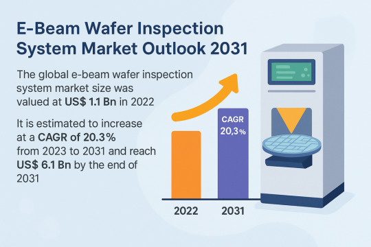
The global e-beam wafer inspection system market, valued at US$ 1.1 Bn in 2022, is projected to grow at a stellar CAGR of 20.3% from 2023 to 2031, reaching a market size of US$ 6.1 Bn by the end of 2031. As the semiconductor industry scales down to ever-smaller nodes and complex 3D architectures, electron beam (e-beam) wafer inspection systems are emerging as critical tools for defect detection and process optimization.
Market Overview: E-beam wafer inspection systems utilize high-energy electron beams to scan semiconductor wafers at nanoscale resolutions. These tools are essential in identifying particles, pattern anomalies, and line-width variations that are undetectable by traditional optical inspection systems. Their increasing application across memory and logic chip production lines highlights their importance in ensuring device reliability and performance.
Market Drivers & Trends
Miniaturization of Semiconductor Nodes: As manufacturers move toward 7nm, 5nm, and even smaller nodes, traditional optical inspection is insufficient. E-beam inspection offers the resolution and sensitivity required for these dimensions.
EUV Lithography Integration: EUV (Extreme Ultraviolet) lithography is now a standard in cutting-edge chip manufacturing. However, it introduces new stochastic defects and patterning challenges. E-beam inspection tools provide essential capabilities to detect these elusive defects early in the production cycle.
Rise of Advanced Packaging: The industry's transition to 2.5D and 3D architectures such as TSV (through-silicon vias) and RDL (redistribution layers) necessitates repeated, high-resolution inspection. E-beam systems are ideally suited for these tasks.
Key Players and Industry Leaders
The competitive landscape includes both established giants and niche innovators. Key players include:
Applied Materials Inc.
ASML Holding N.V.
Hitachi Ltd.
Holon co., ltd.
KLA Corporation
MKS Instruments, Inc.
PDF Solutions
Photo electron Soul Inc.
TASMIT, Inc.
Telemark Factory
ZEISS Semiconductor Manufacturing Technology
Recent Developments
Hitachi Ltd. (2021) launched its GS1000 e-beam inspection system, targeting defect inspection challenges in 3nm and 5nm EUV lithography processes.
KLA Corporation (2020) introduced the eSL10TM, a next-generation e-beam defect inspection platform designed to support rapid development and yield enhancement for EUV-based logic and memory devices.
Download to explore critical insights from our Report in this sample - https://www.transparencymarketresearch.com/sample/sample.php?flag=S&rep_id=15884
Latest Market Trends
A major trend shaping the industry is the rise of multibeam e-beam wafer inspection systems. These systems tackle two core challenges: increasing throughput and improving defect sensitivity. With more beams operating simultaneously, they scan wafers faster while maintaining the precision necessary for advanced nodes. Multibeam technology is expected to gain significant market share in the coming years.
Market Opportunities
The rise in electric vehicle (EV) production, 5G infrastructure deployment, and AI/ML chip manufacturing are fueling demand for semiconductors—and by extension, wafer inspection technologies. Additionally, government-backed initiatives like the CHIPS and Science Act in the U.S. offer a significant boost to semiconductor R&D and domestic production.
Future Outlook
According to analysts, the e-beam wafer inspection system market will continue to experience robust growth due to:
Continuous scaling of device architectures.
Complexity in back-end packaging and integration.
Demand for real-time yield learning and root-cause analysis.
Global expansion of fab capacity in response to chip shortages.
By 2031, multibeam inspection systems are expected to become the default standard for high-volume manufacturing environments.
Market Segmentation
By Type:
Single Beam
Multi Beam (Fastest growing segment)
By Wafer Node:
Mature Nodes (Above 10nm)
Advanced Nodes (10nm, 7nm, 5nm, below)
By Application:
Logic Chips
Memory Chips
Others
By End-use Industry:
Automotive
Consumer Electronics
IT & Telecom
Industrial
Others (Aerospace, Healthcare)
Regional Insights
Asia Pacific dominates the global market, led by powerhouse semiconductor hubs in China, Taiwan, South Korea, and Japan. Rapid expansion in consumer electronics, EVs, and 5G rollout is driving massive investments in chip fabrication and inspection technologies.
North America follows closely, supported by a robust R&D ecosystem, the rise of AI data centers, and federal funding through the CHIPS Act to bolster domestic semiconductor manufacturing.
Europe and South America are emerging as key regions, with growing investments in clean tech, automotive chips, and industrial IoT requiring advanced IC inspection systems.
Why Buy This Report?
Comprehensive Analysis: Covers market dynamics, drivers, trends, and competitive landscape.
Quantitative Forecasts: Value (US$ Bn) and volume (units) projections from 2023–2031.
Company Profiles: Includes strategic insights, product offerings, and recent developments of key players.
Regional Coverage: Provides market insights from major regions and economies.
In-depth Segmentation: Enables clear understanding of sub-market trends.
Frequently Asked Questions (FAQs)
Q1. What is the current size of the global e-beam wafer inspection system market? The market was valued at US$ 1.1 Bn in 2022.
Q2. What is the projected market size by 2031? It is expected to reach US$ 6.1 Bn, growing at a CAGR of 20.3%.
Q3. What are the major growth drivers? Key drivers include shrinking device nodes, EUV lithography adoption, and advanced packaging technologies.
Q4. Who are the major players in the market? Some of the major players include KLA Corporation, Hitachi Ltd., Applied Materials Inc., ASML, and ZEISS SMT.
Q5. Which region leads the market? Asia Pacific currently leads, followed by North America.
Q6. Which segment will grow fastest during the forecast period? The multibeam e-beam inspection system segment is projected to grow the fastest due to its throughput and sensitivity advantages.
Explore Latest Research Reports by Transparency Market Research: Semiconductor Metrology Equipment Market: https://www.transparencymarketresearch.com/semiconductor-metrology-equipment-market.html
Quantum Processing Units (QPU) Market: https://www.transparencymarketresearch.com/quantum-processing-units-qpu-market.html
Solid State Transformer Market: https://www.transparencymarketresearch.com/solid-State-transformer.html
Tactile Switches Market: https://www.transparencymarketresearch.com/tactile-switches-market.html
About Transparency Market Research Transparency Market Research, a global market research company registered at Wilmington, Delaware, United States, provides custom research and consulting services. Our exclusive blend of quantitative forecasting and trends analysis provides forward-looking insights for thousands of decision makers. Our experienced team of Analysts, Researchers, and Consultants use proprietary data sources and various tools & techniques to gather and analyses information. Our data repository is continuously updated and revised by a team of research experts, so that it always reflects the latest trends and information. With a broad research and analysis capability, Transparency Market Research employs rigorous primary and secondary research techniques in developing distinctive data sets and research material for business reports. Contact: Transparency Market Research Inc. CORPORATE HEADQUARTER DOWNTOWN, 1000 N. West Street, Suite 1200, Wilmington, Delaware 19801 USA Tel: +1-518-618-1030 USA - Canada Toll Free: 866-552-3453 Website: https://www.transparencymarketresearch.com Email: [email protected]
0 notes
Text
InGaAs Image Sensors Market Drivers Include Rising Demand for Infrared Industrial Vision Systems
Introduction
Rising automation, stricter quality standards, and the quest for reliable low-light inspection are propelling the InGaAs Image Sensors Market toward unprecedented growth. Made from indium-gallium-arsenide, these sensors capture visible-to-short-wave-infrared (SWIR) wavelengths, making them indispensable for modern industrial vision systems that must see beyond what silicon-based detectors can perceive. The market is expected to grow significantly as manufacturers intensify investments in photonics-enabled production lines.

1. Industrial Vision Systems Lead Demand
The strongest driver is the integration of SWIR cameras into production-floor machine-vision systems. Silicon detectors become ineffective above 1 µm, leaving inspection gaps in semiconductor wafer probing, electrolyte checks in lithium-ion batteries, and mixed-plastic sorting. In contrast, InGaAs arrays can detect moisture, organic compounds, and silicon defects through protective coatings, enabling complete, non-destructive in-line inspection. As automation expands, factories demand sensors that offer high-speed imaging and reliability under harsh operational conditions.
2. Process-Automation Economics: Why Infrared Pays for Itself
SWIR-enabled imaging reduces false rejects and rework by revealing invisible contaminants or layer thickness variations. Automotive paint shops can minimize scrap by identifying solvent pockets, while pharmaceutical production lines using InGaAs systems achieve quick return on investment due to improved defect detection. These gains help justify the higher upfront costs of InGaAs-based solutions, especially in high-volume or high-value manufacturing sectors.
3. Low-Light Advantages and Spectral Selectivity
Unlike thermal detectors that require emitted heat, InGaAs sensors operate in the reflective SWIR band (0.9–1.7 µm), providing high-contrast imaging even under low-light conditions. These sensors can work with invisible, eye-safe LED illumination, making them ideal for around-the-clock inspection. Narrow-band filtering enables detection of specific materials like epoxy, moisture, or sugars, enhancing precision without redesigning hardware, which makes InGaAs a versatile tool across industries.
4. Falling Costs and Technological Breakthroughs
Three major advances are driving costs down:
Improved manufacturing yields – Modern fabrication techniques have increased sensor yields, reducing per-unit cost.
Wafer-level packaging – Integration of micro-optics and signal processing at the wafer level lowers assembly complexity.
Flexible integration – Open firmware and modular architecture allow OEMs to customize performance without incurring licensing costs.
As a result, the total cost of deploying InGaAs-based vision systems is dropping, encouraging broader adoption even in mid-sized industrial operations.
5. Regulatory, Safety, and Sustainability Catalysts
Government regulations now push for non-contact, accurate inspection across industries like food safety, battery production, and chemical handling. InGaAs image sensors meet regulatory expectations for material detection and quality control. They also contribute to sustainability goals by enhancing combustion control in furnaces and kilns, reducing energy consumption and greenhouse gas emissions across industrial operations.
6. Regional Hotspots
Asia-Pacific: Strong manufacturing infrastructure and government subsidies are boosting domestic production and deployment of SWIR systems.
North America: Military and defense applications are accelerating InGaAs sensor demand for field-deployable systems and night-vision solutions.
Europe: Environmental compliance and industrial innovation are encouraging adoption in recycling and automation-focused sectors.
Each region is witnessing demand driven by a unique combination of policy, infrastructure, and sectoral focus.
7. Competitive Landscape
The market is currently dominated by a mix of global and regional players. Larger firms specialize in high-performance, large-format sensors for aerospace and defense, while smaller firms focus on cost-efficient solutions for industrial applications. New entrants are leveraging AI-enabled on-sensor analytics and compact form factors to address emerging use cases like portable diagnostics and mobile inspection.
8. Looking Ahead: What the Drivers Mean for Future Demand
The combination of regulatory mandates, improving economics, and performance advantages makes InGaAs image sensors increasingly attractive across industries. Demand is expanding not only in factory settings but also in outdoor, mobile, and autonomous systems. These sensors are expected to play a central role in future smart manufacturing and automated quality assurance systems.
Conclusion: Setting the Stage for Trends in Night-Vision and Surveillance
While industrial inspection remains a powerful catalyst, the capabilities of InGaAs sensors in low-light and covert environments point toward major growth in night-vision and surveillance applications. In the next article, we explore how these sectors are shaping innovation in sensor design, ruggedization, and real-time data processing.
#InGaAsImageSensors#InfraredImaging#IndustrialVision#SWIR#MachineVision#SmartManufacturing#SensorTechnology#AutomationSolutions#VisionSystems
0 notes
Text
E-Beam Wafer Inspection System : Market Trends and Future Scope 2032
The E-Beam Wafer Inspection System Market is poised for significant growth, with its valuation reaching approximately US$ 990.32 million in 2024 and projected to expand at a remarkable CAGR of 17.10% from 2025 to 2032. As the semiconductor industry evolves to accommodate more advanced technologies like AI, IoT, and quantum computing, precision inspection tools such as E-beam wafer systems are becoming indispensable. These systems play a pivotal role in ensuring chip reliability and yield by detecting defects that traditional optical tools might overlook.
Understanding E-Beam Wafer Inspection Technology
E-Beam (electron beam) wafer inspection systems leverage finely focused beams of electrons to scan the surface of semiconductor wafers. Unlike optical inspection methods that rely on light reflection, E-beam systems offer significantly higher resolution, capable of detecting defects as small as a few nanometers. This level of precision is essential in today’s era of sub-5nm chip nodes, where any minor defect can result in a failed component or degraded device performance.
These systems operate by directing an electron beam across the wafer's surface and detecting changes in secondary electron emissions, which occur when the primary beam interacts with the wafer material. These emissions are then analyzed to identify defects such as particle contamination, pattern deviations, and electrical faults with extreme accuracy.
Market Drivers: Why Demand Is Accelerating
Shrinking Node Sizes As semiconductor manufacturers continue their pursuit of Moore’s Law, chip geometries are shrinking rapidly. The migration from 10nm to 5nm and now toward 3nm and beyond requires metrology tools capable of atomic-level resolution. E-beam inspection meets this demand by offering the only feasible method to identify ultra-small defects at such scales.
Increasing Complexity of Semiconductor Devices Advanced nodes incorporate FinFETs, 3D NAND, and chiplets, which make inspection significantly more complex. The three-dimensional structures and dense integration elevate the risk of process-induced defects, reinforcing the need for advanced inspection technologies.
Growing Adoption of AI and HPC Devices Artificial intelligence (AI) chips, graphics processing units (GPUs), and high-performance computing (HPC) applications demand flawless silicon. With their intense performance requirements, these chips must undergo rigorous inspection to ensure reliability.
Yield Optimization and Cost Reduction Identifying defects early in the semiconductor fabrication process can help prevent downstream failures, significantly reducing manufacturing costs. E-beam inspection offers a proactive quality control mechanism, enhancing production yield.
Key Market Segments
The global E-Beam Wafer Inspection System Market is segmented based on technology type, application, end-user, and geography.
By Technology Type:
Scanning Electron Microscope (SEM) based systems
Multi-beam inspection systems
By Application:
Defect inspection
Lithography verification
Process monitoring
By End-User:
Integrated Device Manufacturers (IDMs)
Foundries
Fabless companies
Asia-Pacific dominates the market owing to the presence of major semiconductor manufacturing hubs in countries like Taiwan, South Korea, Japan, and China. North America and Europe also contribute significantly due to technological innovations and research advancements.
Competitive Landscape: Key Players Driving Innovation
Several global players are instrumental in shaping the trajectory of the E-Beam Wafer Inspection System Market. These companies are heavily investing in R&D and product innovation to cater to the growing demand for high-precision inspection systems.
Hitachi Ltd: One of the pioneers in E-beam inspection technology, Hitachi’s advanced systems are widely used for critical defect review and metrology.
Applied Materials Inc.: Known for its cutting-edge semiconductor equipment, Applied Materials offers inspection tools that combine speed and sensitivity with atomic-level precision.
NXP Semiconductors N.V.: Although primarily a chip manufacturer, NXP’s reliance on inspection tools underscores the importance of defect detection in quality assurance.
Taiwan Semiconductor Manufacturing Co. Ltd. (TSMC): The world’s largest dedicated foundry, TSMC uses E-beam systems extensively in its advanced process nodes to maintain top-tier yield rates.
Renesas Electronics: A leader in automotive and industrial semiconductor solutions, Renesas emphasizes defect detection in complex system-on-chip (SoC) designs.
Challenges and Opportunities
Despite its numerous advantages, E-beam wafer inspection systems face challenges such as:
Throughput Limitations: Due to the nature of electron beam scanning, these systems generally operate slower than optical tools, affecting wafer processing time.
High Capital Investment: Advanced E-beam systems are expensive, which can deter smaller fabs or start-ups from adopting the technology.
However, ongoing innovations like multi-beam inspection systems and AI-powered defect classification are paving the way for faster and more cost-effective inspection solutions. These enhancements are expected to mitigate traditional drawbacks and further fuel market expansion.
Future Outlook
With semiconductors becoming more ingrained in everyday life—powering everything from smartphones to electric vehicles and cloud data centers—the importance of precise defect detection will only intensify. The E-Beam Wafer Inspection System Market is set to benefit tremendously from this surge in demand.
The integration of machine learning algorithms to speed up defect classification, along with the emergence of hybrid inspection platforms combining optical and electron beam technologies, will revolutionize wafer inspection methodologies in the coming years.
In conclusion, the E-Beam Wafer Inspection System Market is not just growing—it’s transforming the foundation of quality assurance in semiconductor manufacturing. As fabrication becomes more intricate and expectations for reliability increase, E-beam systems will remain a cornerstone technology, ensuring the chips that power our digital lives meet the highest standards of performance and precision.
Browse more Report:
Muscle Strengthening Devices Market
Monopolar Electrosurgery Instrument Market
Medical Styrenic Block Copolymers Market
Hard-Wired Commercial Surge Protection Devices Market
Solar Street Lighting Market
0 notes
Text
Automatic Dicing Saw Market Growth Analysis 2025
The global Automatic Dicing Saw market was valued at US$ 567.4 million in 2024 and is projected to reach US$ 785.3 million by 2032, registering a CAGR of 4.6% from 2025 to 2032. This growth trajectory is attributed to the rapid expansion of the semiconductor industry, rising demand for consumer electronics, and technological advancements in wafer processing equipment. The increasing adoption of 5G technology, Internet of Things (IoT), and automotive electronics further contribute to the market's upward momentum. Historically, the market has demonstrated resilience, recovering strongly from disruptions like the COVID-19 pandemic and geopolitical trade tensions. The Asia-Pacific region, particularly China, Japan, and South Korea, continues to dominate the market, owing to its robust semiconductor fabrication ecosystem.

Automatic dicing saws are high-precision cutting tools widely used in semiconductor manufacturing and other high-tech industries. They perform the critical task of cutting silicon wafers, ceramics, and other materials into discrete, functional units. Controlled by advanced software systems, these machines ensure ultra-clean cuts, minimal kerf loss, and high throughput. Depending on the application, automatic dicing saws can handle a variety of materials and dimensions, making them indispensable in fabricating microelectronic components like integrated circuits (ICs), micro-electromechanical systems (MEMS), and optoelectronic devices. The integration of vision systems and robotic automation has further enhanced the efficiency, accuracy, and adaptability of modern dicing saws.
get free sample of this report at https://www.intelmarketresearch.com/manufacturing-and-construction/823/global-automatic-dicing-saw-2025-2032
Market Dynamics (Drivers, Restraints, Opportunities, and Challenges)
Drivers
Booming Semiconductor Industry: The proliferation of smartphones, AI chips, and autonomous vehicle systems is accelerating demand for advanced semiconductor components, thereby driving the need for precise dicing solutions.
Rise in MEMS and IoT Devices: Devices like smart sensors and wearable tech rely on ultra-small components that require highly accurate dicing processes.
Automation and Smart Manufacturing: Industry 4.0 is pushing manufacturers toward automated, software-driven tools for increased efficiency and lower labor costs.
Restraints
High Initial Investment: The cost of fully automatic dicing systems and associated setup can be prohibitively high for small and mid-sized enterprises.
Technical Complexity: The operation and maintenance of these machines require skilled personnel, which can be a barrier in less developed regions.
Opportunities
Emerging Markets: Expanding semiconductor operations in countries like India, Vietnam, and Brazil offer significant growth potential.
Advancements in Vision Technology: Integration of AI and machine learning in vision systems can improve defect detection and operational precision.
Challenges
Supply Chain Disruptions: Trade tensions and raw material shortages can delay manufacturing and increase costs.
Regulatory and Compliance Issues: Adhering to international standards and environmental regulations can pose operational hurdles.
Regional Analysis
Asia-Pacific
The Asia-Pacific region dominates the Automatic Dicing Saw market, led by powerhouses like China, Japan, South Korea, and Taiwan. These countries are home to major semiconductor foundries and OEMs. Japan, for example, hosts leading companies like DISCO Corporation and Tokyo Seimitsu, while China benefits from substantial government-backed semiconductor initiatives.
North America
The U.S. continues to play a critical role due to its innovation-led tech sector and presence of companies like Plasma Therm. The demand for advanced packaging solutions in AI and aerospace sectors propels the market.
Europe
Germany and the UK are pivotal due to their strong industrial base and automotive electronics sector. Companies like Besi from the Netherlands contribute significantly to regional growth.
Rest of the World
Countries in Latin America and the Middle East are gradually increasing their footprint in microelectronics, offering new avenues for market expansion.
Competitor Analysis (in brief)
The Automatic Dicing Saw market features a mix of established players and emerging innovators. DISCO Corporation and Tokyo Seimitsu lead the market with comprehensive product portfolios and global distribution networks. Companies like ADT Corporation, Synova SA, and Kulicke & Soffa bring niche technologies and specialized offerings. Han’s Laser and CETC cater predominantly to the growing Chinese market, while Loadpoint Ltd. and Besi focus on European customers. Strategic partnerships, R&D investments, and product differentiation are key strategies employed to stay competitive.
Global Automatic Dicing Saw Market: Market Segmentation Analysis
This report provides a deep insight into the global Automatic Dicing Saw market, covering all its essential aspects. This ranges from a macro overview of the market to micro details of the market size, competitive landscape, development trend, niche market, key market drivers and challenges, SWOT analysis, value chain analysis, etc.
The analysis helps the reader to shape the competition within the industries and strategies for the competitive environment to enhance the potential profit. Furthermore, it provides a simple framework for evaluating and assessing the position of the business organization. The report structure also focuses on the competitive landscape of the Global Automatic Dicing Saw Market. This report introduces in detail the market share, market performance, product situation, operation situation, etc., of the main players, which helps the readers in the industry to identify the main competitors and deeply understand the competition pattern of the market.
In a word, this report is a must-read for industry players, investors, researchers, consultants, business strategists, and all those who have any kind of stake or are planning to foray into the Automatic Dicing Saw market in any manner.
Market Segmentation (by Type)
Fully Automatic Dicing Saws
Semi-Automatic Dicing Saws
Market Segmentation (by Cagetgory)
Single Spindel
Twin Spindel
Market Segmentation (by Dicing Blade)
Nickel-Bond Dicing Blades
Resin-Bond Dicing Blades
Metal Sintered Dicing Blades
Market Segmentation (by Application)
Silicon Wafer Dicing
Semiconductor Dicing
Glass Sheet Dicing
Ceramic Dicing
Others
Market Segmentation (by End Use Industry)
Electronics & Semiconductor
Military & Aerospace
Telecommunications
Passive Component Manufacturing
Medical Electronics
Others
Key Company
DISCO Corporation (Japan)
Tokyo Seimitsu Co., Ltd. (ACCRETECH) (Japan)
Loadpoint Ltd. (UK)
ASMPT (Singapore/Germany)
Kulicke & Soffa (K&S) (Singapore/USA)
ADT Corporation (Taiwan)
Besi (Netherlands)
Synova SA (Switzerland)
Han’s Laser (China)
CETC (China Electronics Technology Group) (China)
Plasma Therm (USA)
TOKYO WELD Co., Ltd. (Japan)
Geographic Segmentation
North America (United States, Canada, Mexico)
Europe (Germany, UK, France, Italy, Russia)
Asia-Pacific (China, Japan, South Korea, India, Southeast Asia)
South America (Brazil, Argentina, Colombia)
Middle East & Africa (Saudi Arabia, UAE, Egypt, South Africa)
FAQ
▶ What is the current market size of the Automatic Dicing Saw market?
The global market was valued at US$ 567.4 million in 2024 and is projected to grow to US$ 785.3 million by 2032.
▶ Which are the key companies operating in the Automatic Dicing Saw market?
Key players include DISCO Corporation, Tokyo Seimitsu, ADT Corporation, Synova SA, and Kulicke & Soffa, among others.
▶ What are the key growth drivers in the Automatic Dicing Saw market?
Major drivers include the growth of the semiconductor industry, increased demand for MEMS and IoT devices, and rising automation in manufacturing.
▶ Which regions dominate the Automatic Dicing Saw market?
Asia-Pacific leads the market, followed by North America and Europe.
▶ What are the emerging trends in the Automatic Dicing Saw market?
Trends include integration of AI-powered vision systems, automation, and expansion into emerging semiconductor hubs like India and Vietnam.
get free sample of this report at https://www.intelmarketresearch.com/manufacturing-and-construction/823/global-automatic-dicing-saw-2025-2032
0 notes
Text
How does AI Quality Control Redefines Product Quality and Reliability in Fast-Paced Manufacturing ?

AI Quality Control leverages machine learning (ML), computer vision, and predictive analytics to detect defects, optimize processes, and ensure consistent product excellence even in the fastest production environments. This article explores how AI is transforming quality control and setting new benchmarks for product reliability.
The Limitations of Traditional Quality Control
Conventional QC methods face several challenges:
Human Error & Fatigue – Manual inspections are prone to inconsistencies due to human limitations.
Slow Processing Speeds – Traditional systems cannot match the real-time demands of high-speed production lines.
Reactive Rather Than Proactive – Defects are often detected too late, leading to costly recalls and waste.
AI-driven quality control overcomes these hurdles by introducing automation, real-time monitoring, and predictive capabilities.
How AI Enhances Quality Control in Manufacturing
1. Automated Defect Detection with Computer Vision
AI-powered computer vision systems with advanced AI defect detection capabilities use deep learning to analyze thousands of products per minute with superhuman accuracy. These systems can:
Detect microscopic defects invisible to the human eye.
Classify defects by type and severity for immediate corrective action.
Adapt to new product designs without extensive reprogramming.
Companies like Tesla and Foxconn use AI vision systems to inspect electronic components and automotive parts at unprecedented speeds.
2. Predictive Quality Analytics
AI doesn’t just detect defects—it predicts and prevents them. By analyzing historical production data, AI models can:
Identify patterns leading to defects (e.g., machine wear, temperature fluctuations).
Recommend adjustments before defects occur.
Reduce scrap rates and improve yield.
For example, semiconductor manufacturers use AI to predict wafer defects, saving millions in rejected batches.
3. Real-Time Process Optimization
AI continuously monitors production lines and adjusts parameters in real time to maintain optimal quality. This includes:
Automatically calibrating machinery for precision.
Detecting anomalies in sensor data (vibrations, pressure, etc.).
Reducing variability in output for consistent product quality.
The Impact of AI on Manufacturing Quality Standards
✔ Higher Accuracy & Fewer Defects
AI reduces human error, ensuring near-perfect defect detection rates (often >99% accuracy).
✔ Faster Inspections & Increased Throughput
Automated AI systems inspect products in milliseconds, keeping pace with high-speed production without bottlenecks.
✔ Cost Savings & Waste Reduction
Early defect detection minimizes rework, scrap, and recalls, leading to significant cost reductions.
✔ Improved Compliance & Traceability
AI maintains detailed logs of inspections, helping manufacturers comply with stringent industry regulations (e.g., ISO, FDA).
The Future of AI in Quality Control
As AI evolves, we can expect:
Generative AI for Synthetic Defect Training – Simulating rare defects to improve detection models.
Edge AI for On-Device Processing – Faster inspections without cloud dependency.
AI-Driven Supplier Quality Management – Automating QC across supply chains.
Conclusion
AI-powered quality control is revolutionizing manufacturing by setting new standards for speed, accuracy, and reliability. By automating inspections, predicting defects, and optimizing processes in real time, AI ensures that manufacturers can deliver flawless products at scale.
Manufacturers who embrace AI-driven QC today will lead the market tomorrow with higher quality, lower costs, and unmatched efficiency.
0 notes
Text
The Future Of Test Engineering In Chiplet And 3d Ic Architectures

Traditional monolithic designs are giving way to modular chiplet and 3D IC architectures in the semiconductor industry. This change opens the door to further integration and performance opportunities while addressing the escalating problems caused by Moore's Law. These sophisticated systems do, however, present special test engineering difficulties that traditional approaches are ill-equipped to handle. In order to guarantee reliability and performance in these next-generation semiconductor designs, test methodologies must change, as this article examines crucial Quality Engineering Services features for chiplet and 3D IC architectures.
Pre-Bond Testing: The Foundation of Reliable Integration
The crucial initial stage of quality control for chiplet designs is pre-bond testing. Each component needs to be thoroughly inspected to find any possible flaws before the separate chiplets are physically linked. By stopping defective parts from entering the integration process, this step avoids the expensive waste of perfectly good chiplets. In order to handle ever thinner silicon wafers, testing engineers must use specialized probe techniques that can reach smaller test pads. Effective pre-bond testing techniques must be implemented by striking a balance between thoroughness and pragmatism, as too much testing might increase expenses while too little testing could result in dependability problems with the finished product.
Die-to-Die Interface Testing: Ensuring Seamless Communication
Die-to-die interface testing is crucial because the communication channels between chiplets serve as the framework for multi-die systems. Across physical boundaries, these interfaces must consistently transport massive volumes of data at lightning-fast rates while preserving signal integrity. Verifying these interfaces presents special difficulties for test engineers, such as the necessity to replicate real-world operational circumstances and the scarcity of physical access points. Built-in self-test circuits are becoming more and more important, and new ways that combine structural and functional testing approaches are emerging. Test product engineering solutions must constantly modify their methods when die-to-die communication standards change in order to guarantee that these vital interfaces continue to function flawlessly under a variety of circumstances.
Through-Silicon Via Inspection: Navigating the Vertical Dimension
Reliability is crucial to system performance because Through-Silicon Vias (TSVs) act as the vertical highways that connect various layers in 3D IC layouts. These tiny holes drilled into silicon need meticulous production accuracy as well as equally stringent post-manufacturing inspection methods. To find tiny flaws like microvoids, fractures, or misalignments that can jeopardize electrical connection, test engineers use specialized equipment that uses ultrasonic, infrared, and X-ray technology. As TSV dimensions decrease and densities rise, the testing problem becomes more difficult and calls for increasingly advanced detection techniques. Engineers may now confirm TSV integrity during the production process without jeopardizing the structural integrity of these sensitive channels thanks to the ongoing development of innovative non-destructive testing techniques.
Thermal Management Verification: Controlling the Heat Factor
Since heat produced by lower layers is retained by upper layers, the stacked architecture of 3D integrated circuits poses previously unheard-of thermal problems that might result in performance loss or even irreversible damage. Advanced thermal testing techniques that can precisely detect and forecast the temperature distribution throughout the stack while it is operating must be developed by test engineers. Using infrared imaging methods, sophisticated thermal simulation models, and integrated thermal sensors are all part of this. Worst-case power consumption patterns are among the many operational situations that must be taken into consideration throughout the verification process. The validation of dynamic thermal management systems that can modify chip performance in real-time to maintain ideal operating temperatures throughout the whole integrated structure is becoming more and more important to test engineers as chiplet designs get more intricate.
Known-Good-Die Strategies: Maximizing Assembly Yield
The basis for producing chiplets in an economically feasible manner is the known-good-die (KGD) method. The idea is simple but difficult to put into practice: to optimize final assembly yield, thoroughly test and validate each individual die before integrating them. To obtain near-perfect defect detection rates without significantly increasing production costs, test engineers must create specialized wafer-level and die-level test procedures. This entails finding a careful balance between test economics and test coverage. This method is optimized by the use of adaptive test flows, in which test parameters change in response to trends in production data. KGD tactics continue to change as chiplet topologies become more varied, with a growing focus on standardized test procedures that preserve uniformity across different chiplet designs from different manufacturers.
Power Integrity Testing: Ensuring Stable Operation Under Load
The intricate problem of preserving a steady voltage and current distribution across multi-die systems under a range of operating loads is addressed by power integrity testing. There are many possible sites of failure because of the various power needs of distinct chiplets and the intricate power delivery systems required to sustain them. Even during periods of high processing demand, test engineers must confirm that power rails retain the proper voltages without making excessive noise or drooping. This calls for specialized testing apparatus that can concurrently monitor several power domains and replicate real-world power consumption patterns. Test procedures must change when chiplet designs include more complex power management features in order to confirm dynamic voltage and frequency scaling across die borders and guarantee that power-saving measures operate as intended without endangering system stability.
System-Level Testing: Verifying End-to-End Functionality
The final stage of verification is system-level testing, where engineers make sure the integrated chiplet assembly works as intended as a whole. All functional requirements, performance measurements, and reliability indicators of the finished product must be confirmed by this thorough testing process. The difficulty for test engineers is to create test plans that are both economical and comprehensive enough to handle the intricate relationships between many chiplets working together. This frequently calls for specialized test tools and advanced software that can put the system through a variety of operational situations. System-level testing is increasingly using artificial intelligence approaches to detect small performance irregularities and anticipate possible failure causes before they materialize in field circumstances as chiplet-based systems get more complicated.
Conclusion
An interesting intersection of innovation and difficulty exists in test engineering for chiplet and 3D IC pcb board design. Test procedures must keep developing as these cutting-edge designs become more widely used in order to guarantee dependability without causing delays in time to market. The rate of acceptance and eventual success of these ground-breaking semiconductor designs will be greatly impacted by the industry's capacity to work together to create efficient test solutions. The upcoming generation of high-performance computing systems will be made possible by more advanced, automated, and standardized test methodologies.
0 notes
Text
InGaAs Camera Market Unlocking Precision Imaging in Low-Light and Infrared Applications
The InGaAs Camera Market is rapidly gaining momentum as demand rises for high-performance imaging across sectors like defense, industrial inspection, semiconductors, and medical diagnostics. InGaAs (Indium Gallium Arsenide) cameras are specialized sensors capable of detecting short-wave infrared (SWIR) wavelengths, which makes them ideal for low-light and non-visible imaging. According to Market Research Future, the global InGaAs camera market is projected to reach USD 221.3 million by 2030, growing at a CAGR of 8.1% during the forecast period.
Market Overview
Unlike traditional silicon-based sensors, InGaAs sensors are sensitive in the 900 nm to 1700 nm spectral range. This allows InGaAs cameras to "see" beyond the visible spectrum—making them critical in quality control, spectral imaging, laser beam profiling, and military night vision applications.
With global investments rising in defense technologies, semiconductor manufacturing, and advanced industrial automation, InGaAs cameras are seeing robust adoption. In addition, medical and food inspection sectors are utilizing these cameras for their ability to reveal material and structural differences invisible to the human eye.
Market Segmentation
By Camera Type:
Area Scan Camera
Line Scan Camera
By Scanning Type:
Hyperspectral Imaging
Multispectral Imaging
By Cooling Technology:
Cooled InGaAs Camera
Uncooled InGaAs Camera
By Application:
Military & Defense
Industrial Automation
Medical Diagnostics
Spectroscopy
Surveillance
Semiconductor Inspection
Scientific Research
By Region:
North America
Europe
Asia-Pacific
Rest of the World
Key Market Trends
1. Rising Use in Semiconductor Inspection
InGaAs cameras are ideal for wafer inspection and failure analysis in semiconductor production lines. Their ability to detect subsurface defects at the micron level gives manufacturers a crucial edge in quality assurance.
2. Growing Demand in Defense and Surveillance
Governments are integrating InGaAs cameras into night vision devices, border security systems, and drone payloads for enhanced low-light imaging and target detection capabilities.
3. Adoption in Hyperspectral Imaging
The growing popularity of hyperspectral imaging in food safety, mineral mapping, and pharmaceutical testing is expanding the use of InGaAs sensors in lab and industrial environments.
4. Uncooled Cameras Gaining Momentum
Thanks to advances in uncooled sensor design, manufacturers are offering affordable, compact InGaAs cameras that are easier to deploy in commercial settings like machine vision and inspection systems.
Segment Insights
Area Scan Cameras Lead the Market
Area scan InGaAs cameras are widely used for two-dimensional imaging applications in semiconductor inspection, surveillance, and spectroscopy. Their flexibility and high resolution make them suitable for a broad range of use cases.
Hyperspectral Imaging Grows Rapidly
Hyperspectral imaging systems, which collect data across a wide spectrum of wavelengths, benefit immensely from InGaAs sensors. These are increasingly used in applications requiring detailed chemical composition analysis.
Cooled Cameras Remain Vital for Precision
Although more expensive, cooled InGaAs cameras offer higher sensitivity and lower noise, making them ideal for scientific research, astronomy, and defense applications.
End-User Insights
Military & Defense:
InGaAs cameras provide superior night vision and thermal capabilities, making them critical in surveillance, reconnaissance, missile tracking, and laser beam detection.
Industrial Automation:
These cameras are used for process monitoring, detecting defects in high-speed production lines, and verifying product integrity—especially where traditional cameras fail.
Semiconductor Manufacturing:
From wafer inspection to die-level analysis, InGaAs cameras detect defects in silicon and compound semiconductor materials at sub-micron levels.
Medical and Life Sciences:
Used in biomedical imaging and diagnostics, these sensors assist in early disease detection and precision imaging in surgery or laboratory analysis.
Key Players in the InGaAs Camera Market
Several companies are innovating in compact form factor, uncooled variants, high frame-rate performance, and multi-spectral configurations. Key players include:
Teledyne Technologies Incorporated
Xenics NV
Allied Vision Technologies GmbH
Hamamatsu Photonics K.K.
FLIR Systems, Inc.
Sensors Unlimited (a part of Collins Aerospace)
Raptor Photonics
Photonic Science and Engineering Ltd.
New Imaging Technologies (NIT)
FluxData, Inc.
These vendors are also integrating AI-based analytics and cloud-connectivity features to expand use in smart factories and autonomous platforms.
Conclusion
The InGaAs Camera Market stands at the forefront of next-gen imaging, enabling superior performance in environments where visible light sensors fall short. With their unique ability to detect SWIR wavelengths, InGaAs cameras are driving innovations in defense, manufacturing, life sciences, and beyond. As prices continue to fall and applications widen, the market is poised for strong and sustained growth.
Trending Report Highlights
Explore related and emerging markets shaping the future of advanced electronics and automation:
Gyroscope Market
BLE Beacons Market
Audio IC Market
Microcontroller Unit (MCU) Market
Digital Mobile Radio (DMR) Market
Factory Automation Sensor Market
Mining Automation Market
USB Devices Market
AI-Powered Storage Market
Quantum Dots Market
0 notes
Text
Photomask Inspection Market Future Trends Driving Technological Advancements and Quality Assurance Standards
The photomask inspection market is experiencing a transformative shift as technological innovation and miniaturization continue to define the trajectory of the semiconductor industry. Photomasks are essential components in semiconductor manufacturing, serving as master templates for transferring circuit patterns onto wafers. As the complexity of integrated circuits increases, ensuring the accuracy and cleanliness of photomasks becomes more critical than ever. The market is now responding to a rising demand for enhanced inspection methods, integrating next-generation tools and automation to deliver unmatched precision and performance.

One of the most notable future trends shaping this market is the growing adoption of AI and machine learning algorithms in inspection systems. Traditional inspection methods, though effective, often face limitations in identifying ultra-fine defects in complex nanostructures. AI-powered systems, on the other hand, can learn from massive datasets and adapt inspection protocols to detect sub-wavelength defects with higher accuracy and speed. This trend not only minimizes false positives but also reduces the inspection time significantly, making semiconductor manufacturing more efficient.
Another critical trend is the increasing demand for actinic inspection tools. As extreme ultraviolet (EUV) lithography becomes a standard in advanced semiconductor nodes, the need for EUV-compatible inspection systems is growing. Unlike conventional methods, actinic inspection simulates the same wavelength of light used in EUV lithography, thereby ensuring defect detection under real production conditions. This approach provides more accurate insights into potential manufacturing flaws, thereby enhancing quality assurance across the board.
The shift toward 3D NAND and advanced packaging technologies is also pushing the boundaries of photomask inspection capabilities. In the context of 3D integrated circuits and heterogeneous integration, photomasks now require multi-dimensional inspection processes to detect pattern shifts and layer misalignments. Future inspection tools are expected to evolve with improved resolution, depth perception, and adaptability to multi-layer environments. These enhancements will be key to supporting the production of cutting-edge microchips used in AI, cloud computing, and IoT applications.
Additionally, in-line and real-time inspection systems are becoming increasingly popular in modern fabrication facilities. Traditional inspection methods often involve off-line analysis, which may delay feedback and corrective actions. In contrast, real-time inspection allows manufacturers to detect and address defects immediately during the production process. This trend aligns with the broader industry move toward smart manufacturing, where data-driven decisions and automation reduce downtime and optimize yields.
A significant driving factor behind these trends is the need for cost reduction and time efficiency in the semiconductor production process. As the industry progresses toward 2nm and below nodes, photomask costs are escalating due to increasing design complexity and stringent quality standards. Advanced inspection systems can prevent costly reworks and improve first-pass yields, ultimately reducing overall manufacturing expenses. This economic motivation is prompting both manufacturers and tool vendors to invest in R&D and adopt emerging inspection technologies.
Moreover, environmental sustainability is gradually becoming a part of the conversation. With semiconductor fabrication consuming significant energy and resources, there is an increasing push to develop eco-friendly inspection tools. Future photomask inspection systems may incorporate energy-efficient hardware and minimize waste through smarter defect filtering and process optimization. Companies aiming for green manufacturing are likely to favor such sustainable solutions, influencing market dynamics in the years ahead.
On the regional front, Asia-Pacific remains a dominant market, driven by the presence of major semiconductor manufacturing hubs in countries like Taiwan, South Korea, China, and Japan. These nations are at the forefront of adopting cutting-edge lithography and inspection technologies. Meanwhile, North America and Europe are also investing heavily in semiconductor supply chain localization and innovation, further boosting demand for high-performance photomask inspection solutions.
In terms of industry players, the market is seeing both established leaders and innovative startups competing to provide high-speed, high-resolution inspection tools. Strategic partnerships, mergers, and acquisitions are becoming common as companies aim to expand their technological capabilities and market reach. Future competition will likely hinge on advancements in resolution, accuracy, throughput, and system intelligence.
In conclusion, the photomask inspection market is on the brink of a new era, driven by trends such as AI integration, EUV compatibility, 3D packaging support, real-time defect detection, and sustainability. As semiconductor devices become more advanced and miniaturized, inspection systems must evolve to ensure uncompromising quality and efficiency. Stakeholders who adapt quickly to these trends will be best positioned to thrive in this highly competitive and technologically demanding market.
#PhotomaskInspectionMarket#SemiconductorTechnology#EUVLithography#AIinSemiconductors#ChipManufacturing
0 notes
Text
Exploring the Intersection of Metrology and Nano-Technology in Semiconductor Development
As semiconductor technology continues to advance, the demand for smaller, faster, and more efficient devices grows. At the core of this innovation lies the intersection of metrology and nano-technology. These two fields play a vital role in ensuring precision and quality in the development of nano-scale semiconductor devices. In this blog, we will explore how metrology and nano-technology collaborate to drive progress in semiconductor manufacturing.
What does nanotechnology mean in semiconductor development? Nanotechnology is the manipulation of matter on an atomic or molecular size, generally between 1 and 100 nanometers. In semiconductor development, this entails producing smaller, more efficient structures like transistors, which are essential for high-performance devices. As components decrease, nanotechnology enables higher functionality, lower power consumption, and more computing capacity. The role of metrology in nano-semiconductor development Metrology is the science of measurement, and it is used in semiconductor production to ensure that nano-scale structures are manufactured with the required precision. As gadgets shrink, standard measuring methods become ineffective, necessitating the use of increasingly complex technologies. Metrology allows you to measure and verify the precise features of nanostructures, ensuring that each component fits the tight tolerances necessary for peak performance. Key Metrology Techniques for Nano-Semiconductor Manufacturing 1. Scanning electron microscopy (SEM) SEM employs electron beams to create high-resolution pictures of semiconductor wafers. It is critical for examining nanostructures, such as transistor gates, to ensure they meet the specified dimensions and are free of flaws. 2. Atomic force microscopy (AFM) AFM analyzes surfaces at the atomic level, producing high-resolution photographs of nanoscale topography. It aids in the detection of surface roughness and impurities, resulting in uniform and defect-free constructions.
3. X-ray diffraction (XRD XRD measures the crystal structure of materials. In semiconductor production, it is used to test the material characteristics of thin films and discover flaws such as stress or dislocations that might impair device performance. Synergy between metrology and nanotechnology Nanotechnology enables component downsizing, whereas metrology in Semiconductor Industryguarantees that these small structures fulfill rigorous requirements. Manufacturers may use modern instruments like as SEM, AFM, and XRD to correctly measure, examine, and verify each stage of the manufacturing process, resulting in high-performance and defect-free devices.Challenges and Future Outlook As transistor sizes approach the atomic scale, obtaining accuracy becomes increasingly difficult. However, advances in metrology in Semiconductor Industry techniques, like as high-resolution imaging and non-destructive testing, continue to help the semiconductor industry overcome these challenges. Conclusion The convergence of metrology in Semiconductor Industry and nanotechnology is critical to the creation of smaller, more efficient semiconductor devices. Metrology ensures that nanostructures fulfill the demanding requirements necessary for great performance, reliability, and efficiency in next-generation technology.
0 notes
Text
AI-Driven Manufacturing: How Data and Human Intelligence Are Shaping 2025

Manufacturing is going through a major shift. By 2025, smart factories won’t just be a concept, they will define how production happens. This change isn’t just about automation; it’s about using real-time data, AI, and human expertise together to improve manufacturing processes.
The Power Behind Manufacturing
Factories today generate large amounts of data from IoT devices. But raw data isn’t enough — it must be turned into useful insights that improve production.
Better Process Control: Advanced analytics and edge computing help make real-time adjustments. For example, in metalworking, AI can analyze tool vibration and temperature, helping set the right cutting speed and feed rate. This can extend tool life by 20% and improve surface finish by 15%.
Predicting Quality Issues: AI doesn’t just find defects — it can predict when a problem might happen. In semiconductor manufacturing, AI models can spot wafer defects with over 95% accuracy, reducing waste and improving output.
AI: Working Together With People
AI is not about replacing workers — it’s about making better decisions and improving production.
Smarter Robots: AI-powered robots can adjust to different part sizes and shapes, reducing downtime and making production more flexible.
Helping Workers Solve Production Issues: AI systems gather data from various sources, allowing operators to detect and resolve production challenges more quickly.
AI in Product Design: AI-driven design tools can create and test product designs faster, making products stronger, lighter, and easier to manufacture. This is already being used in the aerospace and automotive industries.
Skilled Workers: The Backbone of Smart Factories
Even with all these advancements, experienced workers remain crucial in smart factories. AI and robotics support them, ensuring smoother operations and better results.
Working With Robots: Cobots (collaborative robots) handle repetitive tasks, allowing workers to focus on complex and skilled operations.
AI That Supports Workers: AI systems now explain their suggestions, helping operators understand and make better decisions.
Ensuring Factories Secure and Reliable
With more connected systems, cybersecurity and supply chain risks are growing. Manufacturers need to focus on security to keep operations running smoothly.
Stronger Security Measures: A ‘zero trust’ approach ensures that only authorized users and devices can access factory systems.
Protecting Machines From Cyber Threats: AI-powered monitoring systems track industrial networks to spot unusual activity before it causes problems.
Supply Chain Stability: Data analytics help manufacturers identify risks and build stronger, more flexible supply chains to avoid disruptions.
Manufacturing in 2025: Smarter, Faster, and More Reliable
By 2025, factories will be connected systems where data, AI, and skilled workers work together to improve production. Success will come from using technology wisely, investing in workers, and keeping factories secure. The future of manufacturing isn’t just about automation — it’s about making production smarter, more flexible, and ready for the challenges ahead.
#Predicting Quality Issues#AI-powered robots#Smart Factories#Manufacturing in 2025#thirdeyeai#technology#AI-Driven Manufacturing
0 notes