#PCB Assembly Fabrication
Explore tagged Tumblr posts
Visit Tumblr Blog
Explore Tumblr blogs with no restrictions, modern design and the best experience.
Last Seen Tumblr Blogs


Fun Fact
Tumblr has been providing a Korean-language service since 2013.
Text
Investing in Reliable Electronics Assembly and Fabrication Services is Beneficial
Another benefit is optimizing the process of sourcing PCB devices and fabrication services in a highly cost-effective manner. You can control the budget for the project without any hassles. The flexible PCB cost doesn’t go through the roof. You can keep the expense down. It is more sustainable from a long-term perspective.
#PCB Assembly Fabrication#PCB Assembly#PCB#rigid flex printed circuit boards#flexible pcb#printed circuit board assembly services#printed circuit board company
0 notes
Text
What is a Printed Circuit Board?
Printed Circuit Boards are boards that connect various points together through lines and pads. They allow signals and power to connect between two separate physical devices. While the term “printed circuit board” is typically used, other terms to describe these include “printed wiring board” and “printed wiring card.”

#marketing#investing#finance#branding#pcb circuit#pcb#pc build#pcb assembly#flexible circuit board#pcb board fabrication#pcb circuit design#pcb circuit in Gujarat#pcb design company#Printed Circuit Boards
3 notes
·
View notes
Text
What is PCB Assembly ?
PCB Assembly manufacturer - Hitech Circuits Co., Limited
It’s the step in the manufacturing process in which you populate a blank board with the electronic components needed to make it into a functional printed circuit board. It’s these components that make a board into the circuit that enables an electronic product to function. PCB assembly typically takes place via one of two processes:
1. Surface-mount technology
SMT: SMT stands for “Surface Mount Technology“. The SMT components are very small sizes and comes in various packages like 0201, 0402, 0603, 1608 packages for resistors and capacitors. Similarly for Integrated circuits ICs we have SOIC, TSSOP, QFP and BGA.
The SMT components assembly is very difficult for human hands and can be time taking process so it is mostly done by automated pick and place machine.
2. Through-hole manufacturing
THT: THT stands for “Through hole Technology”. The components with leads and wires, like resistors, capacitors, inductors, PDIP ICs, transformers, transistors, IGBTs, MOSFETS are example.
The component has to be inserted on one side of PCB and pulled by leg on other side and cut the leg and solder it. The THT components assembly is usually done by hand soldering and is relatively easy.
Printed Circuit Board Assembly Techniques
There are only two common PCBA techniques available for use by a PCB designer. The methods are:
1. Automated PCB Assembly Techniques
Generally, this technique employs the use of state of the art machines, which are fully automatic. For example, the surface mount components are worth positioning with the aid of an automated pick and place machine.
Again, reflow soldering is commonly for surface mount components usually done in a reflow oven. An automated solder stencil is also used to apply the solder paste on the PCB.
Finally, high tech inspection machines are used to confirm and check the quality of the PCBA. Some of which include: Automated optical inspection machine (AOI), X-ray inspection machines, etc.
Above all, due to the precise monitoring, control of soldering, no human input and versatile machines.
This technique ensures utmost efficiency, output consistencies, and limits defects.
2. Manual PCB Assembly Techniques
This method is favorite for use with through-hole parts, which needs manual placement on the board. Besides, with these through-hole parts, it’s advisable you use wave soldering. Note that in the through- hole assembly process, you need to place the components and electronics on the PCB.
After that, you use wave soldering to solder the leads. Typically, you will need an individual to insert a component into a marked PTH. Once done, transfer the PCB to the next station where the next person will be on standby tasked with fixing another part.
What are the Benefits of SMT PCB Assembly?
SMT assembly provides many benefits and some of them are as follows:
It can be used to incorporate small components.
In SMT, the components can be placed on both sides of the board.
It assures high component densities.
Fewer holes need to be drilled for surface mounting than through-hole.
It require low initial costs and time for setting up the mass production.
SMT is the simpler and faster-automated assembly when compared to through-hole.
Errors regarding the component placement can be easily rectified.
Surface mount PCBs feature strong joints, which can easily withstand vibrations.
What are the techniques used in Surface Mount Technology?
There are several techniques for the reflow process. After applying the solder paste or a flux mixture on the board and after placing the components, the boards are conveyed to a reflow soldering oven. The techniques used for reflowing soldering include infrared lamps, hot gas convection, fluorocarbon liquids with a high boiling point, and so on.
What are the different testing methods used in SMT PCB Assembly?
Hitech Circuits as the PCB assembly manufacturer, we perform the following testing and inspection to ensure the quality of surface mount PCBs.
Automated Optical Inspection (AOI): This is performed before and after the soldering to identify the component placement, presence, and solder quality.
X-ray Testing: In this type of testing, the operator relies on the X-ray images of the PCB to check the solder joints and lead-less components such as Quad Flat Packs and ball grid arrays, which are generally not visible to naked eyes.
In-Circuit Testing (ICT): This method is used to detect manufacturing defects by testing the electrical properties in the SMT Assembly.
What type of files or documents should I send for SMT PCB Assembly?
Gerber Files: The file contains all details of physical board layers including solder masks, copper layers, drill data, legends, and so on.
Bill of Materials (BOM): This contains information on the list of items needed for the PCB manufacturing and the instructions of manufacturing.
Pick and Place File: This file contains information on all components to be used in the PCB design and their rotation and X-Y coordinates.
The whole process of PCB Assembly
1. Bare board loader machine
The first step in the PCB assembly is to arrange the bare boards on the rack, and the machine will automatically send the boards one by one into the SMT assembly line.
2. Printing solder paste
When PCB on the SMT production line, firstly, we have to print solder paste on it, and the solder paste will be printed on the pads of the PCB. These solder pastes will be melt and solder the electronic parts to the circuit board when it passes through the high-temperature reflow oven.
In addition, when testing new products, some people will use film board/adhesive cardboard instead of solder paste, which can increase the efficiency for adjusting the SMT machines.
3. Solder paste inspection machine(SPI)
Since the quality of solder paste printing is related to the quality of welding of subsequent parts, some SMT factories will use optical machine to check the quality of solder paste after printed the solder paste in order to ensure stable quality. If there any poorly printed solder paste board, we will wash off the solder paste on it and reprint, or remove the excess solder paste if there is redundant solder paste on it.
4. High speed SMT machine
Usually, we will put some small electronic parts (such as small resistors, capacitors, and inductors) to be printed on the circuit board first, and these parts will be slightly stuck by the solder paste just printed on the circuit board, so even if the speed of printing is very fast and the parts on the board will not fall away. But large parts are not suitable for use in such high speed SMT machines, which will slow down the speed of small parts assembly. And the parts will be shifted from the original position due to the rapid movement of the board.
5. Universal SMT machine
Universal SMT machine is also known as "slow machine", it will be assembled some large electronic components, such as BGA IC, connectors, etc., these parts need more accurate positions, so the alignment is very important. Use a camera to take a picture to confirm the position of the parts, so the speed is much slower than High speed SMT machine we taked before. Due to the size of the components here, not all of them are packed in tape and reel, and some may be packed in trays or tubes. But if you want the SMT machine to recognize the trays or tube-shaped packaging materials, you must configure an additional machine.
Generally, traditional SMT machines are using the principle of suction to move electronic parts, and in order to place the parts successfully, and there must be the flat surface on these electronic components for the suction nozzle of the SMT machine to absorb. However, for some electronic parts don’t have a flat surface for these machines, and it is necessary to order special nozzles for these special-shaped parts, or add a flat tape on the parts, or wear a flat cap for thees electronic parts.
6. Manual parts or visual inspection
After assembled all parts by the high speed SMT machine or Universal SMT machine and before going through the high-temperature reflow oven, and we will set up a visual inspection station here and to pick out the deviation parts or missing components boards etc., because we have to use a soldering iron to repair if there are still defectives boards after passing the high-temperature oven, which will affect the quality of the product and will also increase the cost. in addition, for some larger electronic parts or traditional DIP parts or some special reasons cannot be processed by the SMT machine before, they will be manually placed on pcb here.
7. Reflow oven
The purpose of reflow oven is to melt the solder paste and form a non-metallic compound on the component feet and the circuit board, that means to solder electronic components on the circuit board. The temperature rise and fall curves often affect the soldering quality of the entire circuit board. According to the characteristics of the solder materials, usually the reflow oven will set the preheating zone, soaking zone, reflow zone, and cooling zone to achieve the best soldering effect.
For example, the melting point for SAC305 solder paste with lead-free is about 217°C, which means that the temperature of the reflow oven must be higher than the melting points to remelt the solder paste. What's more, the maximum temperature in the reflow furnace should not exceed 250°C, otherwise many parts will be deformed or melted because they cannot withstand such a high temperature.
Basically, after the pcb passed through the reflow oven, the assembly for the entire circuit board is almost complete. If there are hand-soldered parts, we need to transfer to DIP process, and then we have to check the quality after reflow oven by QC department.
8. Automatic optical inspection(AOI)
The main purpose of setting up AOI is because some high density boards can’t be process the following ICT test, so we used AOI inspection to replace it. But even using AOI inspections, there still have the blind spots for such checking, for example, the solder pads under the components cannot be checked by AOI. At present, it can only check whether the parts have side standing issue, missing parts, displacement, polarity direction, solder bridges, lack of soldering etc., but cannot checking the BGA solderability, resistance value, capacitance value, inductance value and other components quality, so far AOI inspection can’t completely replace ICT test.
Therefore, there is still some risk if only AOI inspection is used to replace ICT testing, but ICT test is also not 100% make sure the good quality, we suggest these two ways can be combined with together to make sure the good quality.
9. PCB unloader machine
After the board is fully assembled, it will be retracted to the unloder machine, which has been designed to allow the SMT machine to automatically pick and place the board without damaging the quality for PCB.
10. Visual inspection for finished products
Normally there will be a visual inspection area in our SMT production line whether there is an AOI station or not, and it will help to check if there are any defectives after completed assembled the pcbs. If there is an AOI station, it can reduce the visual inspection worker on our SMT line, and to reduce the potential cost, and because it is still necessary to check some places that cannot be judged by AOI, many SMT factories will provide the mainly visual inspection templates at this station, which is convenient for visual inspection worker to inspect some key parts and polarity for components.
11. DIP process
DIP process is a very important process in the whole PCBA processing, and the processing quality will directly affect the functional for PCBA boards, so it is necessary to pay more attention to the DIP process. There are many preliminary preparations for DIP process. The basic process is to re-process the electronic components first, like to cut the extra pins for some DIP components, our staff received the components according to the BOM list, and will check whether the material part numbers and specifications are correct or not, and performs pre-production pre-processing according to the PCBA samples. The steps are: Use various related equipment (automatic capacitor pins cutting machine, jumper bending machine, diode and triode automatic forming machine, automatic belt forming machine and other machines) for processing.

12. ICT test
Printed Circuit board open/short circuit test (ICT, In-Circuit Test), The purpose of ICT test is mainly to test whether the components and circuits on the printed circuit board are open or short issues. It can also measure the basic characteristics of most components, such as resistance, capacitance, and inductance values to judge whether the functions of these parts are damaged, wrong parts or missing parts etc. after passing through the high-temperature reflow oven.
ICT test machines are divided into advanced and basic machines. The basic ICT test machines are generally called MDA (Manufacturing Defect Analyzer). It’s just to measure the basic characteristics of electronic components and judge open and short circuits issue we talked above.
In addition to all the functions of the basic ICT test machines, for advanced ICT test machine can also test the whole PCBA by using power, start to testing the PCBA boards by setting the program in the test machine. The advantage is that it can simulate the function of the printed circuit board under the actual power-on condition, this test can partly replace the following functional test machine (Function Test). But the cost for the test fixture of this advanced ICT test can probably buy a car, it’s too expensive and we suggest it can be used in mass production products.
13. PCBA function test
Functional testing is to make up for the ICT test, because ICT only tests the open and short circuits on the the PCBA board, and other functions such as BGA and other fuctions are not tested, so it is necessary to use a functional testing machine to test all functions on the whole PCBA board.
14. Cutting board (assembly board de-panel)
Normally, printed circuit boards will be produced in panel, and it will be assembled to increase the efficiency of SMT production. It means several single boards in one panel, such as two-in-one, four-in-one etc. After finished all the pcb assembly process, it needs to be cut into single boards, and for some printed circuit boards with only single boards also need to cut off some redundant board edges.
There are several ways to cut the printed circuit board. You can design the V-cut using the blade cutting machine (Scoring) or directly manually break off the board (not recommended). For more high density circuit boards, it will be used the professional splitting machine or the router to split the board without any damage the electronic components and printed circuit boards, but the cost and working hours will be a little longer.
Why Choose Hitech Circuits PCB Assembly Manufacturer for Your PCB Assembly Projects?
There are several PCB manufacturers specializing in PCB assemblyservices. However, Hitech Circuits PCB Assembly stands out owing to the following:
Assistance in Material Procurement:
Technically, in PCB assembly services, the quality of parts is the responsibility of the OEM; however, we ease your job by assisting you to make the right selection. We can help you procure all your parts of the same type own a single part number, thanks to our supply chain and vendor network as well as experience. This saves time and cost that goes in ordering single parts as you plan.
Testing procedures:
We are very focused on quality and thus implement stringent testing procedures at each stage of the assembly and after completion.
Fast Turnaround Times:
Our well-equipped facility and the right tools enable us to complete your requirements well before time, and without compromising on the quality or functioning of the PCBs. For simple designs we revert in 24 to 48 hours.
Cost Effectiveness:
While PCB assembly is a cost-effective alternative, we go a step further and assure that the parts you list are of a good quality and suitable for your requirement. Also, you can control the part flow and replenish them as needed. This eliminates the need to buy extra stock and store it.
Quick Quote:
We offer a quick quote based on your BOM. All you need is a detailed BOM, Gerber files, your application requirement sheet, and quantity.
We’re not one to stand still, which is why we use the latest equipment and the finest minds to create your PCB projects. We’re constantly keeping our finger on the pulse of the latest trends. And as a result, we know how to deliver the highest standards of PCB assembly to meet all your requirements.
Our dedicated, friendly customer service team also means that we support you every step of the way. Offering our expert guidance to ensure a complete PCB project that you’re happy with.
Contact us today
No matter what your printed circuit board assemblyneeds are, we always aim to deliver efficient, dependable solutions. For more information about our services, do not hesitate to get in touch with us today for a no-obligation quote
2 notes
·
View notes
Text
Tired of Searching for a Reliable PCB Fabrication Company in India? Here’s a Shortcut
If you’ve ever tried to build a piece of hardware—whether it’s a smart gadget, IoT sensor, or your own custom controller board—you know the importance of good PCBs. And let’s be honest, finding a manufacturer you can trust (without going down a rabbit hole of emails, outdated directories, and ghosted quotes) is a nightmare.
That’s why I want to talk about FindingMFG—a business directory that makes finding PCB fabrication company in India actually… easy.
Why India?
India’s electronics scene is booming. From flexible circuits to high-density multilayer boards, Indian manufacturers are now offering world-class capabilities—without breaking your budget.
✅ High-quality manufacturing ✅ Fast prototyping ✅ RoHS & ISO certified ✅ Global shipping ✅ Competitive pricing
So yeah, it’s no surprise that a lot of startups and even big tech companies are moving their PCB sourcing to India.
The Real Problem: Sourcing Sucks
You find a company. Their website looks like it was built in 2009. You email. No response. You try another—minimum order is 10,000 units. Someone else? No capabilities listed at all.
It’s exhausting. And risky if you’re on a tight timeline or budget.
Here’s Where FindingMFG Comes In
FindingMFG is a global business directory for manufacturing—especially electronics and PCBs. It’s basically a smart tool that connects you with verified Indian PCB manufacturers based on exactly what you need.
You can:
🔍 Search by capabilities (HDI, flex, multilayer, etc.) 🛠 Filter by certifications, location, lead time, MOQ 📩 Send out instant quote requests to multiple vendors 🌟 Read real reviews from other users
It’s like Yelp, but for building your next product.
Why It’s a Game-Changer
If you’re a:
Hardware startup
Indie developer
Electronics design student
Product team at a bigger company
...this platform saves hours of sourcing time—and probably a ton of stress, too.
Instead of hoping for the best with a random supplier, you can compare options, check real feedback, and make decisions faster
#pcb fabrication#pcb fabrication companies in india#pcb manufacturing companies#pcb manufacturing companies in India#pcb assembly company#electronics manufacturing
0 notes
Text
What the Future May Have in store for printed circuit board fabrication
The future of electronics is closely tied to innovations in PCB manufacturing company processes, where precision, speed, and customization are becoming key. As technology evolves, companies are investing in smarter solutions to streamline production, meet higher demands, and support rapid development for a range of electronic devices across industries.
Innovation and Speed in PCB Assembly
Modern advancements in Quick-turn PCB assembly are reshaping how we think about electronics production. As demand rises for faster delivery and higher accuracy, manufacturers are incorporating automated systems and AI-driven design to reduce lead times without compromising quality. This evolution is especially critical for printed circuit board fabrication, where reducing time-to-market is a competitive advantage. Connected to this is the growing need for reliable PCB prototype service that ensures these PCB circuits are ready for scaled manufacturing. Businesses now rely on partners that can deliver agility and consistency.
Searching for cutting-edge PCB solutions. Bay Area Circuits offers a suite of services tailored to meet modern demands from prototyping to full-scale production with unmatched precision. Visit their website to explore their services.
To continue reading, Click here - https://bayareacircuits.blogspot.com/2025/04/what-future-may-have-in-store-for.html
#PCB manufacturing company#PCB prototype service#Quick turn PCB assembly#printed circuit board fabrication
0 notes
Text
Viasion Technology Co., Ltd., established in 2007 and headquartered in Shenzhen, China, offers comprehensive PCB solutions, including copper, flexible, and FR4 boards. Their services encompass PCB fabrication, assembly, and electronic manufacturing services (EMS), catering to both small and medium-volume requirements. Viasion's commitment to quality is evident through certifications like ISO 9001:2015 and ISO 13485:2016, ensuring adherence to international standards. With a dedicated team and state-of-the-art facilities, Viasion provides efficient and cost-effective solutions, making them a reliable partner for diverse industries seeking high-quality PCB products.
0 notes
Text

Good luck with your work throughout the new year 🤗 Hope everything at work gets off to a good start~ Welcome to send us the Gerber file and BOM list to our email address: [email protected]
0 notes
Text
China Cable Wire Harness Assembly: Why Topscom Technology is Your Best Choice
In today's fast-paced technological world, cable wire harness assemblies play a crucial role in various industries, from automotive and aerospace to consumer electronics and industrial machinery. These assemblies ensure efficient power transmission, signal connectivity, and overall system reliability. For companies looking to source high-quality cable wire harness assemblies, China has become a prominent global hub due to its advanced manufacturing capabilities and competitive pricing. Among the many providers in China, Topscom Technology stands out as a leading choice for superior China cable wire harness assembly services. https://is.gd/RIk8ag
PCB SMT assembly, China printed circuit board assembly, China PCB factory, China PCB fabrication, China PCB manufacturing, China PCB board, China PCB manufacturer, China PCB service, China PCB prototype, China PCB supplier, China PCB, PCB China, China PCB online, PCB board, China PCB assembly, PCBA China, China PCB design, PCB assembly, China PCB quote, PCBA, contract manufacturing China, China contract manufacturing, contract manufacturing, China electronic assembly, China electronic manufacturing, electronics manufacturing, electronic board manufacturers, China OEM manufacturing, OEM manufacturing, China cable wire harness assembly

0 notes
Text
1 note
·
View note
Text
LHD Technology participated in the 17th AES UAE Home Appliances and Consumer Electronics Show 2024-Made in China Goes Global

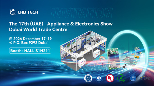
At the upcoming 17th AES UAE Home Appliances and Consumer Electronics Show, we will showcase our expertise in the PCB and PCBA field. As a company with more than 20 years of experience in R&D, production and sales. The following is a detailed introduction of our company, as well as our highlights and expectations at the exhibition.
Company Background
Our company was established in 2003 and is committed to providing customers with high-quality PCB (printed circuit board) and PCBA (printed circuit board assembly) solutions. With many years of industry experience, we have accumulated rich technical knowledge and production capabilities to meet the needs of different customers. Our factory is equipped with advanced production equipment and adopts strict quality control processes to ensure that every product meets international standards.


Main industries
Our products mainly cover the following industries:
Security: Provide reliable circuit board solutions for monitoring equipment.
New energy: Meet the renewable energy developed and utilized based on new technologies.
Home appliances: Provide high-efficiency PCB design and manufacturing for various home appliances.
Military industry: Meet the high standards and high reliability requirements of military equipment.
Exhibition highlights
At this exhibition, we will focus on the following aspects:
Latest technologies and products
We will display the latest PCB and PCBA products, including:
High-frequency and high-speed PCB: Suitable for 5G communication and high-frequency applications.
Flexible circuit board: Suitable for application scenarios with limited space and bending.
Environmentally friendly materials: In response to the global environmental protection trend, lead-free materials and recyclable materials are used.


Live Demonstration and Interaction
We will conduct live product demonstrations and factory video playback at the booth. Welcome all customers to experience our one-stop service. At the same time, we will also arrange professional technicians to answer customers' questions and provide customized solutions.
Business negotiation opportunities.
We also participated in exhibitions in India, Iran, and Hong Kong, serving many customers from all over the world, answering their questions and providing professional services.
This exhibition is a good business negotiation platform. We look forward to establishing connections with potential customers from Dubai and surrounding countries to explore cooperation opportunities. Whether you are looking for new suppliers or want to learn about the latest technology, we welcome you.


Future Outlook
With the development of science and technology, the PCB and PCBA markets are facing new opportunities and challenges. We will continue to be committed to technological innovation and continuously improve production efficiency to meet the growing market demand. At the same time, we also hope to further expand the international market through this exhibition and establish long-term cooperative relationships with more customers.


Conclusion
Thank you for reading our introduction. We look forward to seeing you at the 17th AES UAE Home Appliances and Consumer Electronics Show! Please feel free to visit our booth to talk to our team and learn more about our products. If you have any questions or need further information, please feel free to contact us. Let us work together to create a better future!
Phone:+8615337485501 Email: [email protected]
0 notes
Text
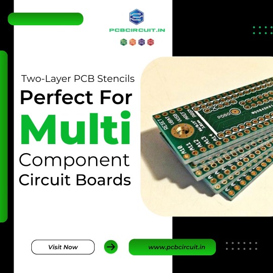
Two-Layer PCB Stencils: Perfect for Multi-Component Circuit Boards
A two-layer PCB stencil is used to assemble printed circuit boards (PCBs) with two layers of copper traces. It helps apply solder paste accurately to the board’s surface before component placement. This stencil ensures precise soldering, reduces defects and improves overall assembly quality. Ideal for both simple and complex circuit designs, it is essential for achieving consistent, high-quality results in PCB manufacturing.
0 notes
Text
We are a professional ceramic pcb manufacturer, supplier from China, we mainly supply high quality Alumina (Al2O3) Ceramic PCB, Aluminum Nitride (AIN) Ceramic PCB board and IGBT Ceramic PCB. Our ceramic printed circuit boards features of high pressure, high insulation, high temperature, and high reliable and minor volume electronic products, Hitech is your best choice for ceramic PCB boards and needs.
0 notes
Text
Finding the Right PCB Fabrication and Assembly Company in India: Powering the Future of Electronics
In the fast-paced world of electronics, every component matters—especially the printed circuit board (PCB). It’s the backbone of every electronic device, from smartphones and smartwatches to industrial machines and medical instruments. That’s why selecting a reliable PCB fabrication company in India or a trusted PCB assembly company in India is a critical step for businesses aiming to produce high-quality products efficiently and cost-effectively.

At FindingMFG, we understand how important it is to find the right manufacturing partner. Our platform bridges the gap between global buyers and India’s top electronics manufacturers, streamlining the sourcing process and ensuring reliability every step of the way.
Why Choose a PCB Fabrication Company in India?
India has positioned itself as a global electronics manufacturing hub, with a rapidly growing ecosystem of PCB fabricators offering cutting-edge technology, competitive pricing, and fast delivery. Many Indian manufacturers now operate with fully automated plants, IPC standards compliance, and global certifications such as ISO 9001 and RoHS.
Here’s why India is an ideal destination for PCB fabrication:
Advanced Capabilities: From single-layer prototypes to complex multi-layer PCBs and HDI boards, Indian companies deliver precision and performance.
Cost Advantage: Get world-class quality at a fraction of the cost compared to Western markets.
Faster Turnaround: Indian manufacturers are known for agile production cycles and on-time delivery.
Custom Solutions: Whether you need rigid, flex, or metal-core PCBs, customization is readily available.
By choosing the right PCB fabrication company in India, companies can reduce lead times, optimize costs, and ensure product reliability.
What Makes a Great PCB Assembly Company in India?
While PCB fabrication builds the board, PCB assembly brings it to life. A top-notch PCB assembly company in India offers end-to-end assembly services, ensuring that every component is placed and soldered with accuracy.
Here are key features to look for:
Full-Service Assembly: Including SMT (Surface Mount Technology), THT (Through-Hole Technology), and mixed assembly.
Component Sourcing: Reliable partners work with authorized distributors to ensure component authenticity.
Quality Control: Automated Optical Inspection (AOI), X-ray inspection, and functional testing reduce the risk of defects.
Box Build Capability: For clients looking for complete product assembly and packaging services.
Partnering with a skilled PCB assembly provider ensures that your final product meets both performance and durability standards.
Why Use FindingMFG?
FindingMFG is more than just a sourcing platform. We simplify your search for a dependable PCB fabrication company in India or PCB assembly company in India by providing:
🌐 A curated list of verified and certified manufacturers
🔍 Instant quote comparison and transparent pricing
🚚 Support for low-volume prototyping to high-volume production
🤝 Global buyer-supplier matchmaking with seamless communication tools
Whether you’re an electronics startup prototyping your first board or an established OEM looking to scale, FindingMFG ensures you connect with the right partners, faster and smarter.
Final Thoughts
As the demand for electronics grows, the need for dependable manufacturing partners becomes essential. Choosing the right PCB fabrication and PCB assembly company in India can make all the difference in your product’s quality, time-to-market, and overall success.
With FindingMFG, you gain access to India’s best electronics manufacturing resources—all in one place. Start your sourcing journey with confidence today
#pcb fabrication company#pcb fabrication company in india#pcb assembly company in india#pcb design#pcb manufacturing company#electronics manufacturing company
0 notes
Text
Printed Circuit Board (PCB) design is a meticulous art that requires precise attention to detail. Central to this process is PCB routing, the sophisticated method of connecting electrical components, defining the pathways for signal propagation within the circuit. This critical phase not only determines the efficiency of signal transmission but also holds the key to signal integrity, which is essential for optimal circuit performance. In this article, we’ll explore PCB routing in depth, highlighting its significance, best practices, guidelines, rules, recommendations, and strategies to ensure you achieve superior signal integrity in your designs.
0 notes
Text
Turnkey Electronics Contract Manufacturing Services, PCB Assembly Services - Topscom
Topscom helps manufacturers of low to medium volume and high volume, high complexity Electronics products focus on the core activities that deliver value to them. We provide complete outsourced manufacturing solutions, provides customers with complete engineering, testing services, and manufacturing resources that are vertically integrated with components to optimize their operations by lowering their costs and reducing their time to markets. https://is.gd/nL4r0T
PCB SMT assembly, China printed circuit board assembly, China PCB factory, China PCB fabrication, China PCB manufacturing, China PCB board, China PCB manufacturer, China PCB service, China PCB prototype, China PCB supplier, China PCB, PCB China, China PCB online, PCB board, China PCB assembly, PCBA China, China PCB design, PCB assembly, China PCB quote, PCBA, contract manufacturing China, China contract manufacturing, contract manufacturing, China electronic assembly, China electronic manufacturing, electronics manufacturing, electronic board manufacturers, China OEM manufacturing, OEM manufacturing, China cable wire harness assembly

0 notes
Text
1 note
·
View note