#PCB edge connector
Explore tagged Tumblr posts
Visit Tumblr Blog
Explore Tumblr blogs with no restrictions, modern design and the best experience.
Last Seen Tumblr Blogs


Fun Fact
After the announcement of the deal with Yahoo!, there were 170K signatures of unhappy Tumblr users petitioning to prevent the sale in 2013.
Text
Type of PCB edge connector, jst connector, harting connectors, PCB edge connector
Z-PACK Series 154 Position 2 mm Pitch Press Fit Through Hole Backpanel Connector
0 notes
Text

Coming soon - USB Plug with THM mounting tabs
We've had some requests to get our Trinkeys soldered up with USB C plugs instead of USB A and like, that turns out to not be trivial! we have to find a USB C plug with through hold tabs so they're nice and strong, and ideally one that isn't "Straddle Mount" where you have to manually place it on the two edges of a PCB. this connector is a nice balance, it has 12 pins so it isn't USB 3.0 but that's OK because right now we're only using USB 2 on our microcontrollers. there's only one CC pin, that's how the upstream can determine orientation. these are more expensive than USB type A but if this works, we can try making some Trinkeys that plug right into modern laptops.
3 notes
·
View notes
Text
Precision and Automation Redefined: Robotic Soldering Station in India – Powered by Ascomp Inc
As the demand for high-speed, precision-based electronics manufacturing continues to grow, manual soldering is no longer sufficient for maintaining consistency, safety, and throughput. Enter the robotic soldering station in India, a powerful innovation that brings automation to one of the most critical steps in PCB assembly. At Ascomp Inc, we supply cutting-edge robotic soldering solutions built for modern Indian factories—designed to enhance productivity, reduce human error, and ensure flawless results.
What is a Robotic Soldering Station?
A robotic soldering station is an automated machine equipped with programmable arms, temperature-controlled soldering tips, and precise motion control systems. It is used to automate repetitive soldering tasks on circuit boards, connectors, and terminal blocks.
Unlike traditional hand soldering, robotic soldering offers:
Consistent solder joints
Reduced operator fatigue
Greater speed and throughput
Lower rework and rejection rates
Better control over temperature and solder feed
Whether you're running a high-volume SMT line or a mid-scale EMS setup, a robotic soldering station in India delivers unmatched accuracy and repeatability.
Key Features of Ascomp Inc’s Robotic Soldering Systems
🤖 Multi-axis robotic arm for precise solder point control
🔥 Temperature-controlled iron tip with programmable profiles
🎯 Vision system and sensors for auto-alignment and inspection
💡 Custom jig fixtures to suit different PCB layouts
🛠️ Automated solder feeding system for consistent wire delivery
⚙️ User-friendly programming interface for custom routines
We also offer fume extraction integration and ESD-safe construction to meet electronics industry safety standards.
Ideal Applications
Our robotic soldering stations are suited for:
SMT and through-hole component soldering
Wire-to-board connections
Connector pin soldering
LED assemblies
Fine-pitch PCB assemblies
Automotive and EV electronics
Telecom and defense equipment manufacturing
Whether you're automating a high-speed production line or improving quality in low-volume, high-precision builds, Ascomp Inc has a model that fits your needs.
Why Invest in Robotic Soldering?
✅ Higher throughput with minimal manual intervention
✅ Lower training and labor costs
✅ Repeatable quality across thousands of units
✅ Fewer operator-related defects
✅ Improved traceability and data logging
It’s not just a tool—it’s a productivity multiplier for forward-thinking electronics manufacturers.
Why Choose Ascomp Inc?
📦 Ready stock of robotic soldering machines in India
🔧 Pre-sales guidance and post-installation support
💼 Integration with existing conveyor or workbench setups
🖥️ Training and programming assistance
🔄 Availability of spare parts and maintenance contracts
🛠️ Proven track record with EMS companies and R&D units
Our solutions are scalable, reliable, and fully customizable based on your board layout and workflow.
#RoboticSolderingIndia#AscompInc#PCBAssemblyTools#ElectronicsAutomationIndia#SMTProductionIndia#AutomatedSolderingStation#IndustrialSolderingRobot#SolderingAutomation#ESDCompliantSoldering#PrecisionElectronicsIndia
0 notes
Text
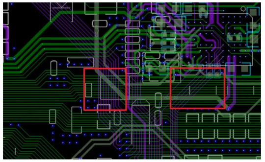
EMC Design Pit Avoidance Guide:
Four no mnemonics
Why does your well-designed product fail EMC testing? The EMC team at Leiditech shares 4 practical EMC design techniques summarized in the “Four No” principles to help you avoid common pitfalls!
Principle 1: Make Current Take the Shortest Path, Not a Detour
Core Logic: High-frequency currents follow the “path of minimum inductance”. Larger loops → stronger radiation!
Key Insights from Leiditech Lab:
l Signal currents must form closed loops, with return paths closely following the outgoing paths.
l Low-frequency (kHz-level) currents follow the “path of minimum resistance”, with possibly dispersed return paths; high-frequency (MHz-level) currents follow the “path of minimum inductance”, with return paths closely adhering to the main trace.
l Design Tip: Place high-speed signals adjacent to their return planes and reduce the spacing between the signal layer and the ground plane.
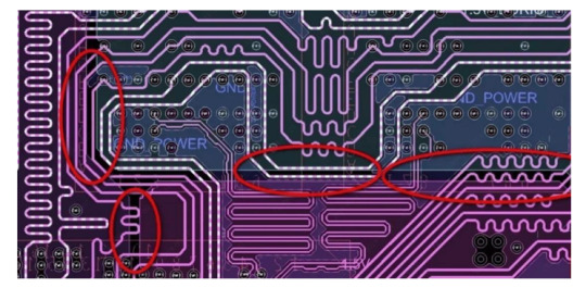
Principle 2: Do Not Split the Signal Return Plane
Leiditech EMC engineers’ golden rule: Provide a complete return plane for all signal currents. For low-frequency signals prone to interference or likely to cause board-level interference, use dedicated trace layers to route return currents back to the source rather than splitting the plane. Arbitrary slotting/dividing the ground plane can cause abrupt changes in return paths → surging EMI!
Exceptions:
Independent return traces may be used only for isolating low-frequency sensitive signals (e.g., audio power supplies), provided:
l The independent layer has a separate return path and does not cross high-frequency planes.
l Consult Leiditech EMC experts to avoid case-by-case misapplication.
Warning: A complete plane is the optimal solution in 99% of scenarios!
Principle 3: Do Not Route High-Speed Circuits Between Connectors
This is one of the most common issues in PCB designs evaluated by Leiditech Lab. Many simple designs that could easily meet EMC requirements (with no extra cost or effort) end up requiring extensive shielding and filtering due to violating this rule.
Why connector placement matters: At frequencies below several hundred MHz, wavelengths can be meter-scale or longer. While the PCB itself acts as a low-efficiency “antenna” due to its small electrical size, cables or external devices connected to the PCB can become efficient radiators.
When signal currents flow on traces and return through a complete plane, the voltage difference between any two points on the plane is typically proportional to the in-plane current. When all connectors are aligned along one side of the PCB, voltage differences between them are negligible. However, if high-speed circuits are routed between connectors, potential differences of several millivolts or more may arise, driving currents into connected cables and causing excessive radiation emissions.

Principle 4: Do Not Blindly Pursue the Fastest Edge; Control Signal Transition Time
Fast edges (1ns) → harmonics up to 2GHz; slow edges (5ns) → harmonics <500MHz.
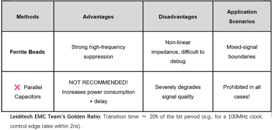
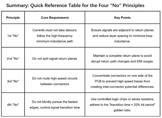
Leiditech EMC Team’s Golden Ratio: Transition time ≈ 20% of the bit period (e.g., for a 100MHz clock, control edge rates within 2ns).
Leiditech Electronics is committed to becoming a leading brand in electromagnetic compatibility (EMC) solutions and component supply. We offer a wide range of products, including ESD, TVS, TSS, GDT, MOV, MOSFET, Zener diodes, and inductors. With an experienced R&D team, we provide personalized customization services to deliver the highest quality EMC solutions tailored to our customers’ needs.
If you’d like to learn more or have any questions, don’t hesitate to reach out: 📧 [[email protected]] 🌐 Visit us at [en.leiditech.com] #NoMoreBuzzing #DriveInPeace #SmartCarTech #ElectromagneticShield #AutoInnovation #CarSafetyFirst #ShanghaiLeditech #NextGenDriving #HornHarmony #AutoElectronics #EMCProtection #StaticNoMore #SmartDriveSolutions
0 notes
Text
Assembly Compatibility of Rigid-Flex PCBs: Challenges and Best Practices
Rigid-Flex PCBs offer mechanical flexibility and space savings, but they also introduce unique challenges during PCB assembly. Unlike standard rigid boards, Rigid-Flex designs often require customized handling, modified assembly procedures, and special fixtures to ensure reliability and manufacturing yield.
This article highlights the key assembly compatibility factors to consider when working with Rigid-Flex PCBs.
1. Handling and Support During SMT
Rigid-Flex PCBs are not flat and rigid throughout. The flexible areas lack structural support, which can cause issues during pick-and-place and reflow processes.
Challenges:
Flex areas may droop or shift during placement
Uneven board thickness requires customized carrier trays
Vibration or vacuum pickup may damage unsupported zones
Best practices:
Use dedicated fixtures or pallets to stabilize the board during SMT
Keep flex zones outside the reflow region if not in use
Avoid placing components too close to flex/rigid transition zones
Use bottom-side supports during reflow to prevent sagging
2. Reflow Soldering Considerations
Rigid-Flex boards often contain materials with different thermal behaviors (e.g., FR-4 and polyimide). This affects reflow performance.
Recommendations:
Use gradual heating profiles to reduce thermal stress between layers
Pre-bake boards before assembly to remove moisture from polyimide (typically 110–125°C for 4–8 hours)
Avoid excessive reflow cycles — confirm your stack-up supports the required thermal budget
3. Component Placement Guidelines
Due to dynamic stress and bending zones, component placement on Rigid-Flex boards requires special attention.
Do not place components or vias in active flex areas
Maintain a clearance buffer zone between components and flex/rigid interfaces (typically 1–2 mm minimum)
Place heavy or high-pin-count components in rigid zones only
Use stiffeners under connector areas to enhance mechanical strength
4. Wave Soldering and Mixed Assembly
If your design involves through-hole components, wave soldering may be used — but only in rigid zones.
Key points:
Flex sections must be protected from heat and physical drag
Consider selective wave soldering or manual soldering for hybrid assemblies
Mask flex areas to prevent contamination or overheating
5. Depaneling and Final Assembly
Rigid-Flex boards often feature irregular outlines, cutouts, and multiple folding lines, which require precise handling.
Use laser cutting or CNC routing for clean edges on both rigid and flex parts
Avoid mechanical shearing that could damage internal layers
During final integration, use controlled folding fixtures to prevent over-bending
If the product requires folding before enclosure assembly, define the correct fold sequence and bend radius in the assembly instructions.
6. Packaging and Transport
Flex zones are mechanically fragile and sensitive to pressure, which makes packaging especially important.
Guidelines:
Avoid stacking boards directly on each other
Use custom foam inserts or anti-static trays with support under rigid areas
Ensure bend zones are kept flat and uncompressed during shipping
7. Documentation and Communication
To ensure smooth assembly, detailed documentation is essential:
Provide 3D drawings showing folding direction and radius
Define "no-go" areas for component placement and tooling holes
Share stack-up data and material specs with the assembler
Clearly label flex areas and handling restrictions on silkscreen or fab drawings
Final Thoughts
Rigid-Flex PCB assembly requires more than standard SMT techniques. From reflow and handling to packaging and integration, each step must accommodate the unique structure and material mix of the board.
By planning ahead, using proper fixtures, and coordinating closely with the assembly house, you can ensure smooth production and maximize the reliability of your Rigid-Flex products.
0 notes
Text
Top Reasons to Buy Electronic Components Online from Semikart
In today’s digital age, the demand for high-quality electronic components is greater than ever — from college students building DIY kits to industries manufacturing cutting-edge technology. But the challenge remains the same: where can you get genuine components quickly, reliably, and affordably?
The answer is simple: Semikart – India’s leading B2B and B2C online platform for sourcing electronic parts.
Whether you're a startup founder, an R&D engineer, a university professor, or a hobbyist, here’s why Semikart should be your go-to source for electronic components.
Top Reasons to Choose Semikart
1. Largest Selection of Components in India
Semikart brings together over 10 million+ electronic parts from global suppliers. You’ll find everything from:
Integrated Circuits (ICs)
Sensors
Microcontrollers
Connectors
Power supplies
RF modules
PCBs and much more
Whether you’re sourcing parts for IoT devices, automation systems, robotics, or general electronics — you’re covered.
2. Only Genuine and Certified Products
At Semikart, authenticity is a priority. All components are sourced from authorized distributors and reputed brands like Texas Instruments, STMicroelectronics, Microchip, NXP, and many more. You get guaranteed quality and performance — no duplicates, no second-hand stock.
3. Simplified Online Buying Experience
The user-friendly website offers:
Smart filters
Powerful search
Real-time inventory status
Technical specifications
Datasheets This helps both first-time buyers and professionals find the right part — fast and easy.
4. Real-Time Availability & Competitive Pricing
No more guesswork. With Semikart, you see live stock levels and actual pricing. Transparent rates and clear availability help you make informed decisions and avoid unnecessary delays.
5. Bulk Orders & Business Support
If you’re running a business or managing procurement, Semikart offers support for:
Volume discounts
Custom quotes
Scheduled deliveries
GST invoicing
Supply chain support
Perfect for OEMs, research institutes, and product design companies.
6. Quick Delivery Across India
Semikart ensures fast shipping to all regions, including metros, Tier-2, and Tier-3 cities. Thanks to their reliable logistics partners, your order is delivered safely and on time.
7. Technical & Customer Support
Have questions about compatibility or specs? Semikart has a dedicated support team ready to help with technical queries, order updates, and post-sales service. They also provide datasheets and helpful advice for selecting the right components.
8. Support for Students, Startups & DIYers
Semikart is not just for big businesses. It’s also a perfect place for:
Students building college projects
Makers designing prototypes
Hobbyists working on DIY gadgets With easy search, low MOQs (minimum order quantities), and budget-friendly pricing — it’s beginner-friendly too.
Conclusion
If you're looking for a reliable, all-in-one solution for electronic components, look no further than Semikart. With a wide product range, trusted quality, bulk order support, and excellent customer service, Semikart has everything you need to bring your electronic ideas to life.
Visit www.semikart.com today and experience a smarter way to source electronics online!
Frequently Asked Questions (FAQs)
Q1: Is Semikart only for bulk or industrial buyers?
No, Semikart caters to both individual and business customers. Whether you need a single resistor or thousands of microcontrollers, Semikart can help.
Q2: Are the products on Semikart genuine and new?
Yes. Semikart sources all components directly from trusted manufacturers and authorized distributors. You always get brand-new, original products.
Q3: Can I track my order after purchase?
Absolutely. Once your order is shipped, you’ll receive tracking details to monitor the delivery status.
Q4: Does Semikart ship all over India?
Yes. Semikart delivers to all major cities and towns across India with fast and secure shipping.
Q5: Do they offer GST invoices?
Yes. You can get a GST-compliant invoice, which is helpful for business purchases and tax purposes.
Q6: What if I need technical help?
Semikart offers pre-sales and post-sales technical support to help you choose the right components and answer any product-related questions.
#semikart#buy online electronics components#components#electronic parts distributor#electronic components distributor#electronics#electronic component suppliers#distributor for electronic components#best electronics components
1 note
·
View note
Text
Transmission Line Impedance Measurement by BitWise Laboratories

BitWise Laboratories is a trusted name in advanced signal integrity testing, offering highly precise transmission line impedance measurement services for engineers, manufacturers, and R&D teams. In high-frequency environments—such as RF circuits, high-speed digital PCBs, and microwave communication systems—accurate impedance matching is crucial. Even minor mismatches can result in signal reflection, loss, and performance degradation. That’s why BitWise Laboratories is committed to delivering accurate, reliable, and high-resolution impedance analysis to support your design goals.
We use cutting-edge tools like Time Domain Reflectometry (TDR) and Vector Network Analyzers (VNA) to analyze impedance characteristics across a wide frequency range. These techniques allow us to detect discontinuities, mismatches, or anomalies in transmission lines, connectors, vias, and traces. Whether you're working on PCB layout, cable design, or integrated system testing, our measurements help ensure your signal path is optimized for efficiency and reliability.

Our clients span industries such as aerospace, automotive, telecommunications, consumer electronics, and defense. Each project is handled by experienced engineers who understand the complex interactions between materials, geometry, and signal behavior. With quick turnaround times, detailed reports, and application-specific recommendations, BitWise Laboratories empowers your team to design and deliver better-performing products.
In today’s competitive electronics landscape, robust signal performance isn’t optional—it’s essential. That’s why companies around the world rely on BitWise Laboratories for mission-critical transmission line impedance measurement that drives quality and compliance. Whether you're prototyping or doing production validation, we bring the expertise and tools necessary to catch issues early and optimize for performance.
From coaxial cables and differential pairs to microstrip and stripline configurations, we help you maintain impedance control from source to load. When signal integrity matters, every ohm counts—and so does every measurement.
Partner with BitWise Laboratories for precision testing, insightful analysis, and the peace of mind that your design is built on solid, measurable foundations.
For more information
Visit us :https://bitwiselabs.com/
0 notes
Text
How to Choose the Right Manual Fixture for Your Testing Needs: A Step-by-Step Guide
In the world of electronics testing and precision manufacturing, the right tools can make the difference between flawless performance and costly rework. Among those tools, the manual fixture plays a pivotal yet often underrated role in ensuring quality, consistency, and efficiency. Whether you're testing PCBs, wiring harnesses, or microelectronic components, selecting the ideal manual fixture is crucial for optimizing test results and minimizing downtime.
But with countless configurations, materials, and functions available, how do you determine which fixture is best suited for your testing environment?
In this guide, we’ll break down the key steps and considerations to help you choose the perfect manual fixture for your specific needs—whether you’re a test engineer, production manager, or quality control specialist.
Step 1: Define Your Testing Objectives Clearly
Before exploring fixture options, clarify what you want the fixture to accomplish. Are you focused on functional testing, continuity testing, or high-voltage isolation? Will it be used in a high-volume production environment or for prototype verification?
Understanding your goals will help narrow down the required features, such as:
Contact type (spring-loaded pins, pogo pins, etc.)
Force requirements
Number of test points
Load/unload speed
At Equip-Test, manual fixture solutions are available for everything from standard bed-of-nails setups to fully customized designs tailored to specific PCB layouts and test flows.
Step 2: Assess the Component or Board Geometry
Next, evaluate the physical characteristics of the unit under test (UUT):
What are the dimensions of the board or component?
Are there connectors or edge contacts?
Does the test require double-sided probing?
These factors will influence the fixture’s platform size, the arrangement of test probes, and whether a top-side pressure plate or vacuum hold-down is necessary.
Equip-Test offers both standard and modular manual fixture systems, making it easier to accommodate complex board geometries without reinventing the wheel every time.
Step 3: Choose the Right Probing Technology
One of the most critical aspects of a manual fixture is the selection of test probes. Depending on the signal integrity, current rating, and pitch requirements, you might need:
Standard spring-loaded probes for through-hole or SMT pads
High-frequency probes for RF circuits
Kelvin probes for low-resistance measurements
Special probes for surface wear or sensitive contacts
Don’t overlook the importance of probe life cycle and accessibility, especially in high-throughput environments.
Equip-Test's vast test probe catalog is engineered to support virtually every test scenario imaginable, ensuring precision and durability.
Step 4: Factor in Ergonomics and Operator Safety
Manual fixtures should not only be functional but also comfortable and safe to use. Consider:
Lever mechanisms or pneumatic assist for high-contact-count boards
Clear visibility and easy access to the DUT
Built-in ESD protection
Shielding for high-voltage applications
A poorly designed manual fixture can increase operator fatigue and error rates. Ergonomic enhancements also reduce the risk of repetitive strain injuries during continuous operation.
Step 5: Plan for Scalability and Maintenance
If your test needs might change in the near future, it’s wise to invest in a modular or upgradable fixture. Look for designs that allow:
Easy probe replacement
Interchangeable probe plates
Quick fixture swaps for different board versions
This is where modular fixture platforms from Equip-Test really shine. These fixtures can be easily reconfigured or upgraded, providing flexibility without excessive downtime or new tooling costs.
Step 6: Work with a Trusted Fixture Manufacturer
Even with a clear checklist, designing the perfect fixture isn’t always DIY-friendly. Partnering with a company that specializes in test fixture development ensures:
Optimal layout and mechanical design
High-quality materials and build
Fast turnaround and support for modifications
Integration with test equipment (ICT, functional testers, etc.)
Equip-Test has been at the forefront of manual fixture solutions for years, supporting global electronics manufacturers with robust, reliable test platforms. Whether you're outfitting a new production line or upgrading legacy systems, their engineering team brings unmatched expertise to every custom fixture build.
Final Thoughts: Precision Starts at the Fixture
Your test equipment is only as good as the connection it makes with the unit under test—and that connection starts with a well-chosen manual fixture. By carefully considering your application requirements, board design, probe technology, ergonomics, and future needs, you can ensure accurate, repeatable test results while keeping costs under control.
Ready to explore your options or need expert advice? Visit Equip-Test to discover high-performance manual fixtures designed to elevate your testing process from the ground up.
0 notes
Text
Socket mount wire, PCB mounted connectors, Socket mount, PCB edge connector
DTM Series 12 Position Dual Row Male Pin Right Angle Header Connector
0 notes
Text
What Makes Proto PCBs and Rigid Flex Circuit Boards Key to Efficient Electronics Manufacturing?
When an gadgets grows, the choice of printed circuit board (PCB) is critical for the usefulness, execution and lifetime of the last item. These components are instrumental in optimizing the generation prepare, empowering faster advancement cycles, and giving more strong, space-efficient plans. Understanding the parts of Proto PCBs and Rigid Flex Circuit Boards in cutting edge electronics can offer assistance manufacturers streamline their forms and progress item quality.
Proto PCBs: The Establishment of Prototyping and Innovation
Proto PCB, too known as prototype PCBs, serve as the to begin with cycle in the PCB improvement cycle. They are basic in the plan and testing stages of item improvement, advertising manufacturers a way to test circuits and components some time recently full-scale generation. Proto PCBs are regularly created in little amounts, permitting engineers to rapidly distinguish plan imperfections, troubleshoot issues, and refine the circuit layout.
One of the fundamental points of interest of Proto PCBs is the speed at which they can be fabricated and tried. Since they are utilized for prototyping, manufacturers can make fast cycles, guaranteeing that the last item is as optimized as conceivable. This flexibility permits companies to decrease advancement time, cut costs, and eventually bring items to showcase faster.
Additionally, Proto PCBs offer the advantage of flexibility in plan. They can be customized to meet the particular needs of a extend, whether that’s for a straightforward buyer gadget or a complex mechanical framework. With progressed manufacturing strategies, Proto PCBs can join high-density interconnects (HDI), fine-pitch components, and multi-layer plans, making them perfect for cutting-edge electronic products.
Rigid Flex Circuit Boards: A Idealize Mix of Rigid and Flexible Technologies
Rigid Flex Circuit Boards speak to a noteworthy progression in PCB design. As the title proposes, they combine the properties of both Rigid PCBs and Flexible circuits, making them profoundly flexible and space-efficient. These Boards are essentially utilized in applications where space is restricted, or the item requires a combination of both Rigid and Flexible connections.
One of the essential benefits of Rigid Flex Circuit Boards is their capacity to give high-density interconnection in compact spaces. These Boards can diminish the number of connectors and cables required in a framework, rearranging the by and large plan. This is especially valuable in businesses such as aviation, car, and restorative gadgets, where estimate, weight, and unwavering quality are vital factors.
Rigid Flex Circuit Boards coordinated Rigid PCB areas with Flexible segments, permitting for both inflexibility in particular regions and adaptability where essential. This crossover plan is perfect for applications that require both steadiness and the capacity to twist or crease in a few parts of the product.

Moreover, these circuit Boards are cost-effective in the long run. Whereas the beginning setup costs might be higher than standard PCBs, Rigid Flex Circuit Boards diminish the require for extra connectors, cables, and other components, driving to investment funds in both get together and upkeep. Their capacity to coordinated numerous capacities into a single board encourage decreases the complexity of the last design.
Enhancing Manufacturing Efficiency
Both Proto PCBs and Rigid Flex Circuit Boards contribute to the by and large proficiency of the gadgets manufacturing prepare. Proto PCBs speed up the prototyping stage, permitting companies to rapidly test and repeat on their plans. This diminishes the hazard of expensive blunders amid the mass generation stage and empowers manufacturers to meet tight deadlines.
On the other hand, Rigid Flex Circuit Boards streamline the last item plan, making a difference manufacturers decrease the number of components, streamline gathering, and upgrade item strength. By coordination both Rigid and Flexible components into a single board, Rigid Flex Circuit Boards make more compact and effective plans, which is a key advantage in today’s gadgets market.
In conclusion, Proto PCBs and Rigid Flex Circuit Boards play a significant part in making strides the effectiveness of gadgets manufacturing. They empower quicker prototyping, more dependable plans, and space-efficient arrangements, all whereas diminishing generation costs. As the request for more modern and compact electronic gadgets develops, these innovations will proceed to be at the cutting edge of development, guaranteeing that manufacturers can meet the challenges of present day gadgets generation.
0 notes
Text
Learning blender to improve the case on my own.
With rapid prototyping now sorted out, I've started learning blender myself to try and make edits to the case easily. It's been slow progress so far, with my friend George coaching me on different things to expand my currently limited blender experience. I've decided to keep the top of the case the same, as it needs no editing and the design is both functional and looks good visually.
This means I needed to edit the bottom of the case, and by using the extrude tool, along with learning how to dissolve faces and add cubes, I evolved the case over 5 designs, with iterative testing with a half made slimevr to test fit everything.
Here is a picture of all of my prototypes I did myself, i'll explain how I went iterating them over time.


Version 1 The first thing i noticed was how in prototype 2, my batteries were being pierced by the sharp edges formed after trimming down the solder joints, and how the battery had no proper place to sit, so that's the first thing I tried to Improve. By adding a small barrier around the inside of the case to let the battery drop down into it. I printed this version and the bottom of the case pierced from being too thin.

Version 2
All I did in this version was make the bottom of the case thicker, which fixed the issue of it piercing. Although the large sharp corners dug into my skin when tested with a strap over the case.

Version 3
I changed the bottom of the case to use a smaller platform to thicken the bottom of the case, I also added a small cutout to the side of the barrier, to allow for the cables of the battery to go out to the top, as I planned to switch to 2 pin JST connectors for the battery, and they could not fit in the bottom of the case due to there not being enough space.


Version 4 I made the cutout bigger and lower down, as in my testing there was not ample enough space for the cable of the battery to fit through. I also removed 2 out of the 3 standoffs, as they kept snapping off in my testing and fitting the PCBs inside of the cases. I still needed one to keep the PCB stable and in-place.

Version 5 I added small standoffs to every corner, to make sure the PCB would not pierce the battery anymore while maintaining space to easily fit into the hole. This design has worked well since I made it, and I plan to make all of the trackers with this design as I believe it will be durable and long-lasting.

0 notes
Text

Precision Masking for Perfect Plating 3M™ Circuit Plating Tape 1280
3M™ Circuit Plating Tape 1280 – the industry-trusted solution for masking during gold finger plating and PCB edge connector processing. This tape delivers: ✔️ Sharp masking lines ✔️ Excellent conformability ✔️ Clean removal without residue ✔️ High-temperature resistance Perfect for: 🔹 Printed circuit board (PCB) plating 🔹 Edge connector masking 🔹 Wave solder masking
📦 Bulk orders available – DM us or call to get the best price!
📞 Contact Today : +919810987429 📥 Enquire Now : [email protected]
0 notes
Text
Absolute EMS and the Evolution of Next-Gen PCB Assembly Services
The assembly of electronics is a vast, evolving field, filled with challenges. Automation has sparked a quiet revolution in the industry, and it continues to shift in that direction. Within this constantly changing horizon of electronics assembly - precision, reliability, and efficiency drive advancement. Absolute EMS, a leader in PCB Assembly Services (PCBA or EMS), offers cutting-edge assembly solutions to demanding high-performance OEMSs. Their technological expertise in press-fit connectors in silicon valley guarantees a strong interconnect without the inconveniences inherent in conventional soldering.

The Engineering Behind Press-Fit Connectors
Press-fit connectors are a replacement for conventional soldered connections, providing a very reliable mechanical and electrical interface. The connector pins have compliant sections that form a gas-tight joint when pressed into plated through-holes (PTHs) of a PCB. The process provides:
Uniform Contact Pressure: Uniform pressure inside the hole is delivered through elastic deformation of the flexible pin, keeping the micro-movements low and signal attenuation low.
Elimination of Soldering Defects: Defects such as cold joints, solder bridges, and thermal stress are fully eliminated.
Superior Mechanical Retention: High insertion pressure and frictional locking avoid removal by shock and vibration.
Improved High-Frequency Signal Integrity: The uniform contact resistance minimizes electromagnetic interference (EMI) and ensures reliable data transmission in RF and high-speed digital circuits.
Complementary High-Precision PCB Assembly Techniques
Absolute EMS also integrates other cutting-edge methodologies in PCB assembly, ensuring adherence to stringent industry standards such as IPC Class 3 for high-reliability applications. These capabilities include:
High-Density Surface Mount Technology (SMT): Advanced pick-and-place systems handle micro-BGAs, fine-pitch QFNs, and 01005 components for compact, high-performance designs. And large BGA (4k+ balls) pick and place.
Selective Through-Hole Technology (THT): Precision-controlled soldering techniques, including wave soldering and selective soldering, enhance the integrity of mechanical and power connections without disturbing other components on the board..
Hybrid Assembly Solutions: A combination of SMT and PTH and that enables complex multi-layer PCB configurations suited for demanding applications.
Automated Optical Inspection (AOI)and X-Ray Inspection: Ensuring defect-free assembly through real-time analysis and verification of solder joints, component placement, and internal structure.
Final Thoughts
For companies looking for Electronic Manufacturing Services , Absolute EMS provides specialized solutions in press-fit connectors, based in Silicon Valley. They constantly strive to deliver the best technology and their dedication to quality, efficiency, and technology makes them a go-to partner for all the high tech OEMS in Silicon Valley and beyond.
To see their entire range of PCB assembly services, contact Absolute EMS and learn how they can get your product to market faster with their electronic manufacturing processes.
0 notes
Text
Price: [price_with_discount] (as of [price_update_date] - Details) [ad_1] Mini Cool Edge IO. The 0.60mm pitch connector come with a slim form factor design, capable of transmitting high-speed signal up to 64G PAM4/PCIe Gen 4/PCIe Gen 5/PCIe Gen 6, and allowing much greater signal path lengths while maintaining SI performance when compared to conventional pcb routing methods. Mini Cool Edge IO not only provides a SI performance ready signal transmission but also a new way of system design that is cost-effective, highly modular, scalable, and extremely easy to repair. 0.60mm pitch, vertical and right angle configurations;Slim form factor for compact data center system designs Up to 64Gb/s PAM4, PCIe Gen 4, PCIe Gen 5, PCIe Gen 6, over 1.0 meter transmission distance;Extends transmission range far more over the conventional PCB routes Supports both cable and card edge applications with one identical connector;Provides flexibility in system design to meet highly modular, scalable and easy-to-repair requirements Optional for 92Ω (G42 series), 85Ω (G97/GH01X series) and 95Ω (G98 series) impedance and various pin number options - meeting PCIe/NVMe/SAS/SFP(+)/QSFP specifications;Saves system material cost, engineering and certification expenses with high succession of system design [ad_2]
0 notes
Text
The Advantages and Applications of Flexible PCB in Modern Electronics
Introduction
The electronics industry is constantly evolving, and one of the most significant advancements in recent years has been the widespread adoption of Flexible PCB (Printed Circuit Board) technology. Unlike traditional rigid PCBs, Flexible PCB offers unparalleled adaptability, making it ideal for modern compact and high-performance devices. From consumer electronics to medical equipment, Flexible PCB has revolutionized how circuits are designed and implemented.
This article explores the benefits, applications, and future trends of Flexible PCB, highlighting why it has become a cornerstone of innovation in electronics.
What is a Flexible PCB?
A Flexible PCB is a type of printed circuit board made from flexible materials such as polyimide or polyester. Unlike rigid PCBs, which use fiberglass, Flexible PCB can bend, twist, and fold without breaking, enabling more versatile designs.
Key Components of a Flexible PCB
Substrate Material – Typically polyimide, known for its heat resistance and flexibility.
Conductive Layers – Copper traces that form the electrical pathways.
Protective Coating – A coverlay or solder mask to shield the circuits from damage.
Adhesives – Used to bond layers together while maintaining flexibility.
Advantages of Flexible PCB
1. Space and Weight Reduction
One of the biggest advantages of Flexible PCB is its ability to fit into tight spaces. Since it can bend and conform to different shapes, it eliminates the need for bulky connectors and wiring, reducing both size and weight. This makes it perfect for smartphones, wearables, and aerospace applications.
2. Enhanced Durability
Flexible PCB can withstand vibrations, shocks, and repeated bending, making it more durable than rigid PCBs. This is particularly useful in automotive and industrial applications where reliability is critical.
3. Improved Signal Integrity
With fewer interconnects and shorter signal paths, Flexible PCB reduces electromagnetic interference (EMI) and signal loss. This is essential for high-frequency applications like 5G devices and advanced medical imaging systems.
4. Cost-Effective Assembly
Although Flexible PCB may have higher initial material costs, it simplifies assembly by reducing the need for connectors and additional wiring. This leads to lower labor costs and improved production efficiency.
5. Thermal Management
Polyimide-based Flexible PCB can handle high temperatures, making them suitable for applications where heat dissipation is crucial, such as LED lighting and power electronics.
Applications of Flexible PCB
1. Consumer Electronics
Flexible PCB is widely used in smartphones, tablets, and laptops, enabling slimmer designs and foldable screens. Companies like Samsung and Apple rely on Flexible PCB for their cutting-edge devices.
2. Medical Devices
In the medical field, Flexible PCB is used in wearable health monitors, implantable devices, and diagnostic equipment. Its lightweight and biocompatible properties make it ideal for patient-friendly solutions.
3. Automotive Industry
Modern vehicles incorporate Flexible PCB in dashboard displays, sensors, and lighting systems. Its ability to endure harsh environments ensures long-term performance.
4. Aerospace and Defense
Flexible PCB is crucial in satellites, drones, and military equipment due to its lightweight nature and resistance to extreme conditions.
5. Industrial Automation
Robotics and industrial machines use Flexible PCB for reliable signal transmission in dynamic and high-stress environments.
Future Trends in Flexible PCB Technology
1. Stretchable Electronics
Researchers are developing stretchable Flexible PCB that can expand and contract, opening new possibilities for wearable tech and biomedical applications.
2. Integration with IoT
As the Internet of Things (IoT) grows, Flexible PCB will play a key role in connecting smart devices with minimal space requirements.
3. 3D Printed Flexible Circuits
Advancements in 3D printing may allow for custom Flexible PCB designs with even greater complexity and efficiency.
4. Eco-Friendly Materials
Sustainable Flexible PCB materials, such as biodegradable polymers, are being explored to reduce electronic waste.
Conclusion
The rise of Flexible PCB has transformed the electronics industry by offering unmatched flexibility, durability, and efficiency. From smartphones to space technology, its applications are vast and continually expanding. As innovation progresses, Flexible PCB will remain at the forefront of electronic design, enabling smarter, lighter, and more resilient devices.
For engineers and manufacturers, adopting Flexible PCB technology is not just an option—it’s a necessity for staying competitive in a rapidly evolving market.
1 note
·
View note