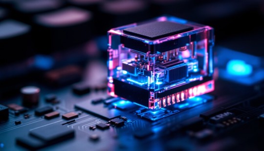
#PCBFabrication
Explore tagged Tumblr posts
Visit Tumblr Blog
Explore Tumblr blogs with no restrictions, modern design and the best experience.
Last Seen Tumblr Blogs


Fun Fact
Tumblr.com rank in the US is 25.
Text
The Future of Electronics Starts with the PCB — And It’s Being Built in India
Behind every smartphone, drone, EV, or IoT device, there’s one common core: the Printed Circuit Board (PCB). Often overlooked, yet absolutely essential, PCBs are the unsung heroes of the modern world.
If you're developing a new tech product, here's something you need to know: India is quickly becoming the global hub for PCB fabrication and assembly.
What is PCB Fabrication?
PCB fabrication is the process of manufacturing the actual circuit board — the foundation that holds and connects all electronic components. It involves precise steps such as:
Layering copper and substrate materials
Etching pathways
Drilling and plating vias
Applying solder masks and silkscreens
Electrical testing and inspection
A top-tier PCB fabrication company in India provides quality manufacturing that meets international standards, all while remaining cost-effective and scalable for startups or mass production.
What is PCB Assembly?
Once the board is fabricated, it’s time for PCB assembly — the process of placing and soldering components like resistors, capacitors, and microcontrollers onto the board. Assembly involves:
Surface Mount Technology (SMT)
Through-Hole Technology (THT)
Component placement automation
Reflow soldering and inspection
Functional testing and quality control
A reliable PCB assembly company in India will ensure your product functions flawlessly from the start, and can scale as your demand grows.
Why India is the Smart Choice
Here’s why companies across the globe are turning to India for their PCB needs:
1. Skilled Engineering Talent India has a vast pool of trained professionals with deep expertise in electronics manufacturing and design.
2. State-of-the-Art Facilities Leading PCB companies in India operate world-class cleanrooms and production lines equipped with high-speed SMT machines and automated testing tools.
3. Competitive Costs Get high-quality PCBs at globally competitive prices — without compromising reliability or delivery speed.
4. Fast Prototyping and Mass Production Indian companies support both small-batch prototyping and high-volume orders with quick turnaround times.
5. Compliance and Quality Most Indian manufacturers follow international standards (ISO, IPC, RoHS), ensuring your boards are ready for export or high-performance applications.
Who Needs a PCB Partner in India?
If you're building or scaling a product in any of these industries:
Consumer Electronics
Industrial Automation
Electric Vehicles
Medical Devices
Aerospace and Defense
Telecommunications
IoT and Wearables
Then partnering with a PCB fabrication and assembly company in India could dramatically reduce your time-to-market while keeping production costs under control.
Final Thoughts
The electronics industry is evolving fast. To stay competitive, you need speed, precision, and reliability — right from the circuit board up. By working with a top-tier PCB fabrication or assembly company in India, you're investing in a foundation that’s built for innovation.
India isn't just manufacturing PCBs. It's powering the next generation of technology
#PCB#ElectronicsManufacturing#TechStartup#ProductDesign#PCBIndia#PCBAssembly#HardwareStartup#Innovation#ElectronicsEngineering#PCBFabrication#IndustrialDesign#MadeInIndia
1 note
·
View note
Text
Experience the future of product innovation with Auckam Technologies. Our advanced embedded systems and precision PCB prototyping services help startups, OEMs, and product developers build smarter, faster, and more efficient electronics. From concept to production, we offer complete electronics design and manufacturing services tailored to industrial, medical, and IoT applications.
🚀 Visit www.auckam.com for custom embedded solutions and full-stack product engineering.
#EmbeddedSystems#PCBFabrication#ProductEngineering#IoTSolutions#ElectronicsDesign#HardwareDevelopment#PrototypeToProduction#SmartDevices#CustomPCBDesign#IndustrialAutomation#MedTechInnovation#AuckamTechnologies
0 notes
Text

#pcbassembly#pcba#PCB#pcbdesign#pcbdesigner#PCBlayout#pcblayoutdesign#pcbfabrication#pcbproduction#pcbprototype#smt#pcbmanufacturing#china#IC#components#electronics
1 note
·
View note
Text

The term PCB corrosion means the degradation or deterioration of printed circuit boards (PCB) due to various factors such as exposure to moisture, contaminants, or chemical reactions. There are some circuit board corrosion cleaner tools and materials available on the market that will help you with cleaning a printed circuit board, but it is recommended that someone with a fundamental knowledge of electronics should attempt to clean a PCB. Before you start cleaning the corrosion on the PCB, you should first disassemble the board and avoid damaging the components. When you separate the PCB from an electronic, stay away from water and disconnect the device.
0 notes
Text
Best PCB Assembly Services in India
Pcbcircuit is one of the best printed circuit board assembly Services providers and manufacturer companies based in India. Printed circuit board Assembly work in tandem with engineers and other electronic professionals. We offer printed circuit board assembly services and PCB Assembly manufacturer services with 100% quality guarantee.

#circuit board assembly#branding#investing#marketing#PCBAfactory#ComponentsSourcing#electronics#projects#pcbfabrication#PCBAManufacturer#PCBmanufacturer#PCBAservice#printedcircuitboaards#PCBassembly#productionworkshop#PCBboards#electronicsmanufacturer#electronicmanufacturingservice#electroniccontractmanufacturing#custom
0 notes
Text
#PCBDesign#CopperCladLaminate#ElectronicsEngineering#CopperFoil#PCBFabrication#CircuitBoards#PCBManufacturing#CopperPlating#HighPowerPCB#IPCStandards#PCBTechnology#HeavyCopperPCB#ElectronicsIndustry#usa#europe#germany
0 notes
Text
PCBA Details Display!!!
#pcb#pcba#pcblayout#pcbfabrication#pcbdesign#pcbassembly#SMT#DIP#BGA#electronics#component#USB#ledboard#aluminum#pcbboard#IC#power#supply#Bluetooth#HDI#sports#headset#flex pcb#fpcway#fpcway.com#flexible circuit board#today on tumblr#rigid-flex pcb#flex circuit pcb#flexible pcb board
0 notes
Text
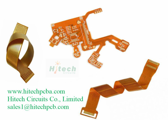
What is Flex PCB?
Flexible printed circuits, also known as flex circuits, are sometimes regarded as a printed circuit board (PCB) that can bend, when in reality there are significant differences between PCB’s and flex circuits when it comes to design, fabrication and functionality. One common mistake that designers make is to design a flexible circuit using the same rules as a PCB. Flex PCB require a unique set-up and have their own set of design rules that the Hitechpcb team has termed “flex-izing” and have worked hard to perfect over the last many years.
Flexible PCB, which also called Flex PCB, Flexible circuit board or flex circuit, it consists of PI base material, adhesive layer, copper layer, coverlay and sometimes with stiffeners. Flexible PCBs are now being used widely to replace traditional FR4 PCB in various different applications due to the benefits from flex PCB specially. Although more expensive than a normal rigid PCB, the right design in the right application could save weight and time in assembly, coupled with the reliability which makes flexible circuit board a worthwhile consideration.
A flexible printed circuit consists of a metallic layer of traces, usually copper, bonded to a dielectric layer, usually polyimide. Thickness of the metal layer can be very thin (<.0001″) to very thick (> .010″) and the dielectric thickness can vary from .0005″ to .010″. Often an adhesive is used to bond the metal to the substrate, but other types of bonding such as vapor deposition can be used to attach the metal.
1 note
·
View note
Text
See how a PCB amazing!
1 note
·
View note
Text
How to realize to get the best Green Power?
To realize getting the best Green Power, consider the following factors:
Renewable energy source: Look for green power that is generated from renewable energy sources, such as wind, solar, or hydroelectric power.
Certification: Choose green power that has been certified by reputable organizations, such as Green-e or the Center for Resource Solutions, to ensure that it meets high environmental and social standards.
Carbon footprint: Consider the carbon footprint of the green power you are considering, including the emissions associated with its generation, transportation, and distribution.
Price: Compare prices of different green power options to ensure that you are getting the best value for your money.
Customer service: Look for a green power provider that offers excellent customer service and support, including transparent billing and easy account management.
Availability: Check the availability of green power in your area, as it may not be available in all regions.
Integration with existing power supply: Consider how the green power will integrate with your existing power supply, including any necessary upgrades or modifications.
One-Stop Service: PCB & PCBa supplier.
Feel free to contact: +86 13430761737,(WhatsApp/WeChat/Skype)
#pcbassembly#pcbdesign#pcba#pcb#pcbmanufacturing#pcbfabrication#pcbsupplier#pcblayout#pcbfactory#pcbuild#pcbprototype#pcbboard#pcbchina#pcbsmt#pcbs#electroonic#electricals#smd#Circuitboard#SMT#pcbService#pcbProduction#PCBAcompany#circuitBoardDesign#circuitMaker#doubleSidedPcbManufacturer#hdiPcbManufacturer#multilayerPcbManufacturer#NewProductDevelop#PrintedCircuitBoard
3 notes
·
View notes
Video
instagram
Posted @withrepost • @pcbgogo_official PCBGOGO factory are doing PCB flying probe testing now. You could see it is a PCB prototype normal tester. ——————————————————————— 📌Register at our website: https://www.pcbgogo.com/member/register ——————————————————————— 📌PCB Instant Quote : https://www.pcbgogo.com/pcb-board-quote.html #pcb #pcbgogo #printcircuitboard #pcbprototype #pcbassembly #pcbmanufacturing #pcbfabrication #smd #soldermask #soldering #silkscreen #wireless #raspberrypi #drone #arduino #arduinofun #arduinoproject #electronics #electronicengineering #diyelectronics #sensor #iot #iotproject #hardware #capacitor #resistor (at Busan, South Korea) https://www.instagram.com/p/B08NpzbHT0V/?igshid=714wmmmv49oe
#pcb#pcbgogo#printcircuitboard#pcbprototype#pcbassembly#pcbmanufacturing#pcbfabrication#smd#soldermask#soldering#silkscreen#wireless#raspberrypi#drone#arduino#arduinofun#arduinoproject#electronics#electronicengineering#diyelectronics#sensor#iot#iotproject#hardware#capacitor#resistor
1 note
·
View note
Text

#pcb#pcba#pcbdesign#pcbdesigner#PCBlayout#pcblayoutdesign#pcbfabrication#pcbproduction#pcbprototype#smt#pcbassembly#pcbmanufacturing#china#IC#components#electronics
0 notes
Text
Everything that You Need to Know About PCB Fabrication!
The first step in the PCB fabrication process is to create a design for the circuit. This typically involves using a computer-aided design (CAD) program to create a schematic diagram of the circuit, which shows the connections between the various components.
Source url: https://pcbsales.substack.com/p/everything-that-you-need-to-know
0 notes
Text
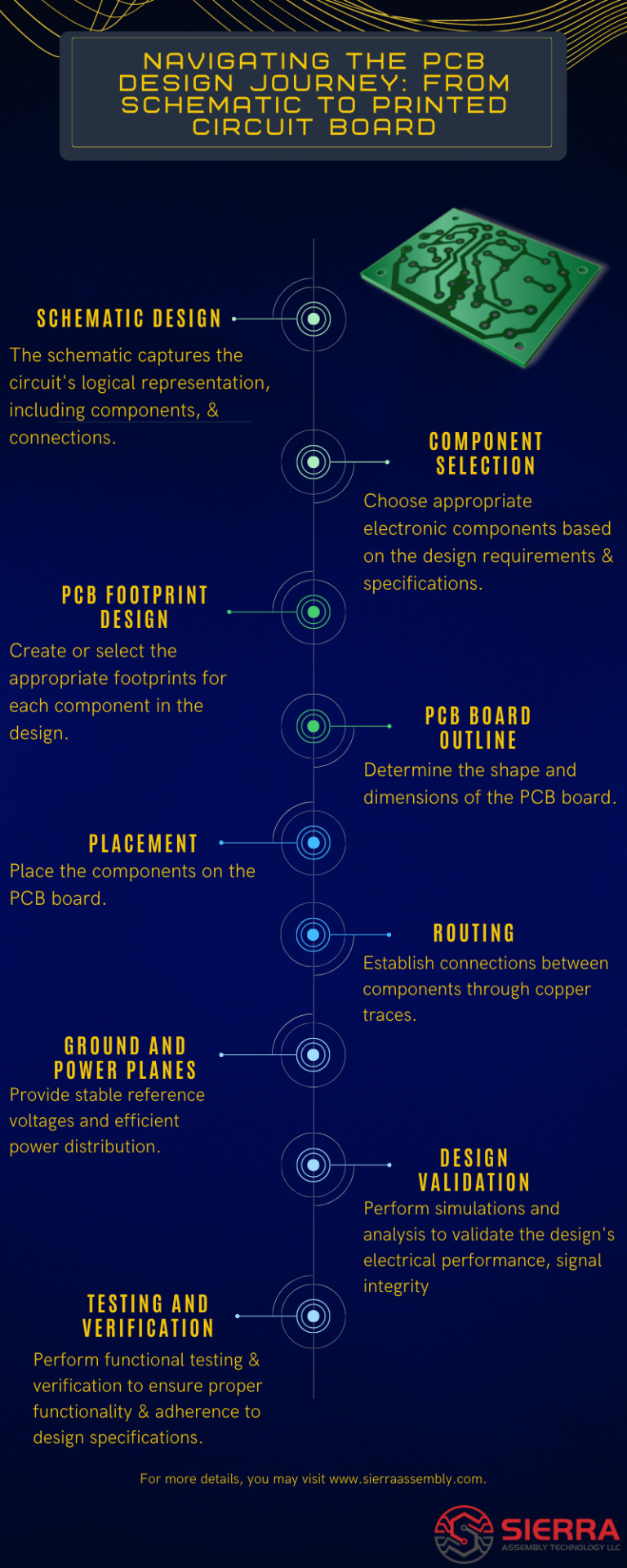
The #PCBdesign journey can be challenging, but it is also incredibly rewarding. The PCB (Printed Circuit Board) design journey refers to the process of creating a PCB, which is a crucial step in the development of electronic devices. It begins with requirement analysis, where the specifications and constraints of the PCB are gathered. Overall, the PCB design journey involves careful planning, schematic design, layout creation, fabrication, assembly, and testing to bring a functional #PCB to life.
1 note
·
View note
Text
Tips for RF PCB Design
With so many things to consider when designing an RF PCB, it can be hard to know where to start. How do you choose the right layout? What tools should you use to get the job done? RF PCB design has its own set of challenges that need to be addressed to get the most out of your circuit. There are some best practices you can use to ensure that your design will function optimally and run smoothly.
The best PCB design solution can be the difference between success and failure for your product, so you want to make sure that you are getting it right the first time around. Our guide will walk you through all of the steps necessary to create an RF design that works and that makes your product even better than you envisioned.
Surface Mount Capacitors
Use surface mount capacitors when space is limited. You can incorporate them into your RF Printed Circuit Board design with no impact on performance. Try to keep track of how much space they’ll take and make sure there’s still enough room for other components on the board, like resistors and coils. The surface mount parts are more fragile than through-hole components and require an extra level of care when handling.
Consider using larger surface mount parts wherever possible, or incorporating test points into any sensitive areas if smaller parts are required. Remember that small surface-mount parts have very thin leads that could break off easily. Make sure you know what size of solder tip will be needed before moving forward with your design. If it’s too small, it could damage the delicate leads on these devices. It may also be difficult to attach them to boards after soldering as their leads are so small that they tend to slide around during assembly. When in doubt, use a slightly larger part.
Differential Pair Transformer Coupling
Choosing proper circuit components is an important part of designing and building circuits. When creating transmitter/receiver pairs, several factors influence how well each device will perform. The goal of any transmitter or receiver circuit is to accurately convert an input voltage into an output voltage with minimal noise and distortion.
These parameters are known as gain, linearity, bandwidth, noise figure, NF, return loss, RL, and intercept point, IP. A low NF results in more power being transferred from input to output. The IP value represents how much power can be handled by the front end of a given device before distorting or saturating it, all while maintaining its linearity characteristics.
In other words, if a device has high gain but poor linearity, then it may still have acceptable levels of IP. But if a device has high gain and poor linearity at lower power levels, then it won’t have good IP numbers. In general, devices with higher gains have lower bandwidths, however, there are exceptions to every rule. For example, some amplifiers have very high gains but also operate over wide frequency ranges.
Microstrip Transmission Lines
These are transmission lines in which all of their circuit elements, including those forming half-space planes, and terminations, such as capacitors and transformers, are fabricated on metal strip circuits. The strip circuit is usually etched onto an epoxy substrate using photo etching or electroplating techniques. The micro-strip designs have become very popular for many PC BOARD applications because they can be packaged in small cases with relative ease due to their thin profile. They also have good impedance matching properties over a wide frequency range.
Reference Planes, Power Planes & Ground Planes
Radio-frequency circuit boards or RF designs are often more sensitive to ground loops and signal integrity issues than regular designs because RF circuits and components are particularly susceptible to noise. One way that experienced designers combat these types of issues is by strategically adding power planes, reference planes, and ground planes to their board layouts.
Reference planes: The reference or signal planes can allow designers to focus on specific sections of a circuit without having to worry about interfering signals from other portions.
They also provide a convenient place for designers to add vias between layers of copper, which helps improve both signal quality and thermal performance. Reference planes can be especially useful when they’re directly connected to a component’s ground pin, which allows them to act as an extension of that component’s ground plane.
Power planes: They should always be connected directly to an external source of power, otherwise, they could cause voltage drops across adjacent traces and components.
Ground planes: They should always be connected directly to an external source of the earth, otherwise, they could cause the voltage rises across adjacent traces and components. It's important to note that many high-speed applications use multiple ground planes at different potentials, so it may not be feasible to have just one global ground plane. However, it's generally best practice to keep each section within a single board connected through at least one shared global ground plane.
By using separate grounds for different sections of a design, designers can avoid parasitic effects and increase the overall reliability by ensuring all parts of their designs have access to low impedance paths back to an external earth point.
In addition, it’s crucial to ensure that any ground or power planes are spaced far enough away from any active circuitry in order to minimize crosstalk. Generally speaking, there should be at least 1/10th of a millimeter between active circuitry and any nearby reference or power planes. The distance requirements become even more stringent with higher frequencies. When operating above 30 GHz, there should ideally be no less than 0.3 mm of separation between any ground or power plane and active circuitry.
Vias – Size, Shape & Placement
Vias are required in order for us to make electrical contact with traces on different layers. There are three types of vias, including plated through, blind, and buried. A plated through via connects one layer’s copper trace directly with another via’s copper trace or traces. A blind via creates electrical contact but no physical connection between two layers and a buried via provides both an electrical and physical connection.
Placement is generally determined by where it will be soldered or how many layers are involved. For example, if there are four or more layers involved then we recommend using plated through vias because they offer better conductivity than a blind via. If there are only two layers involved then we recommend using either type of visa, depending on its location relative to other components.
As far as shape goes, choose from square, round, or rectangular options that match your pcb fabrication layout requirements. Circular vias may also be available upon request, however, these have a higher cost associated with them due to their complexity and are not always necessary. We use wire-bondable vias wherever possible because they provide a faster assembly process. The above diagram illustrates each type of via along with its respective shape and size.
Isolating an RF trace
It is essential to isolate an RF trace from high-speed signals, including HDMI, USB differential pairs, or crystals’ clock traces. Experts do it through a method known as via stitching where vias are stitched around the RF traces to keep them away from other parts on the circuit board. But, there should be proper isolation as improper isolation can affect PCB function.
RF Circuit Board Insulation
Insulation is one of the most important factors for minimizing the signal loss in an RF transmission. If you want to ensure that your signal reaches its destination without any hiccups or interference, it’s crucial that you use good quality material for your board's insulation, and choose one with at least 5-mil thickness.
One of our favorite options is Taconic TFEP as it offers superior heat resistance and can withstand temperatures as high as 350 degrees Celsius. It also has great mechanical properties and will last for years to come. Another great option is Rogers, which boasts similar properties but has a slightly higher temperature resistance.
You'll also want to make sure that you're using a good adhesive when attaching components to your board. This will ensure that everything stays intact even in tough conditions. If you want to ensure that your signal reaches its destination without any hiccups or interference, it’s crucial that you use a good, quality material for your board's insulation.
You can create a flawless RF circuit board by considering all the above design guidelines.
Final Thoughts
RF PCB design has its own set of challenges that need to be addressed in order to get the most out of your circuit. There are some best practices you can use to ensure that your design will function optimally and run smoothly. You have to consider material, traces, surface mount capacitors, isolation, insulation, reference, ground, and power planes, vias size and shape, coupling, and micro-strip transmission line.
Would like to know more about RF design or pcb assembly services? Email us at [email protected]
Website: https://pnconline.com/ Facebook: https://www.facebook.com/PNCONLINE Twitter: https://twitter.com/PNCINC Instagram: https://www.instagram.com/pnc_pcb/ Tumblr: https://www.tumblr.com/blog/view/pncinc Myspace :https://myspace.com/pncinc2020 Bresdel: https://bresdel.com/pncinc Call us: (973) 284-1600 Email us: [email protected] Location: PNC INC, 115 East Centre St.Nutley, NJ, 07110
0 notes
Link
Printed circuit board (PCB) fabrication is a method of assembling circuit boards used in computers and other electronic products in which the various layers of the circuit board are combined together with a specific surface pattern so that it can be used for electronic manufacturing. As the one of PCB fabrication companies in China, HX can manufacture PCB in-house or outsource it to an company that specializes in manufacturing.
Features of PCB Fabrication
Printed circuit board (PCB) fabrication is a method of assembling circuit boards used in computers and other electronic products. The layers of a circuit board are put together along with a specific surface pattern so that it can be used for electronics manufacturing. PCB fabrication companies can manufacture PCBs in-house or outsource this aspect of production to a specialist. PCB fabrication process begins with design. Some PCB fabrication specialists can also design the board, using specifications provided by the customer.
In other cases, customers develop their own files and send them to the PCB fabrication manufacturers. These files are presented in a format called Gerber file, an industry standard for recording PCB-specific details. PCB fabrication companies use Gerber files to program PCB manufacturing for their devices. A variety of techniques can be used, depending on the need for production. Custom products tend to be more expensive because they require small production runs, while generic or standard formats are less costly.
Prototypes, produced in very limited quantities of boards, can be very expensive. And in some cases, to limit PCB fabrication cost and reduce the loss of proprietary information, the conductive foil layers are glued together before being covered with solder masks This is the basis for connecting the thin copper wires of the circuit and can be done by plating or other means. Multiple layers can be made using certain PCB fabrication methods. The finished PCB is assembled with other components and tested to confirm that it works properly before being sent to the customer.
PCB Fabrication Process
The PCB fabrication is a complex process that begins with a product concept and ends with a fully functional PCBA. Here is a sequence of steps of the PCB fabrication process, total of eight steps, generated by PCB fabrication companies.
Step 1 – The Design.
Step 2 – Printing the Design.
Step 3 – Creating the Substrate.
Step 4 – Printing the Inner Layers.
Step 5 – Ultraviolet Light.
Step 6 – Removing Unwanted Copper.
Step 7 – Inspection.
Step 8 – Laminating the Layers.
0 notes