#Printed Circuit Board Manufacturers
Explore tagged Tumblr posts
Visit Tumblr Blog
Explore Tumblr blogs with no restrictions, modern design and the best experience.
Last Seen Tumblr Blogs


Fun Fact
Tumblr.com rank in the US is 25.
Text
PCB Manufacturing in Toronto: Expertise, Services, and Local Industry Insights
Discover PCB manufacturing in Toronto, a hub of innovation and quality in electronic manufacturing services. Learn about the specialized capabilities, technological advancements, and diverse offerings of PCB manufacturers Toronto. Explore how local expertise and cutting-edge facilities contribute to producing high-quality printed circuit boards for various industries and applications worldwide. For more details visit our website www.crimpcircuits.com
#pcb manufacturing toronto#printed circuit board design#metal clad pcb#printed circuits#rigid flex pcb#full turnkey pcb services#turnkey pcb services#pcb parts#eagle software#pcb designing#flexible pcb#pcb assembly#printed circuit board manufacturers#pcb manufacturers in canada#circuit board manufacturers in canada#pcb quote#pcb prototype services in canada
2 notes
·
View notes
Text
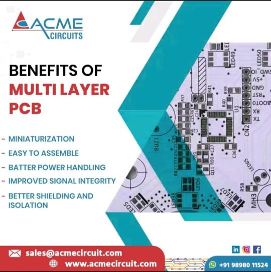
Multilayer PCBs (Printed Circuit Boards) offer numerous advantages over their single-layer or double-layer counterparts. These benefits arise from their enhanced design capabilities, improved performance, and greater flexibility. Here are some key advantages of multilayer PCBs:
#PCB#printed circuit board manufacturers#electronic cable assembly#pcb manufacturing#pcb assembly manufacturer#pcb assembly services#pcb board manufacturer#printed circuit board manufacturer in india#circuit board manufacturing#pcb exporters#pcba#pcb manufacturer#pcb design#pcbassembly#multilayer pcb
2 notes
·
View notes
Text
Electronic devices surround us in all aspects of our lives. From smartphones to advanced medical equipment, we use electronic devices at every point in our lives. Every modern device has a PCB at the center of its design.
0 notes
Text
Trusted PCB Manufacturing in the USA | High-Quality PCB Production & Custom Solutions

Looking for reliable PCB manufacturing in the USA? PCB Power is a trusted PCB board manufacturer known for its advanced technology and high-quality PCB production services. With expertise in both prototyping and large-scale production, they deliver printed circuit boards that meet stringent industry standards. PCB Power offers quick turnaround times, thorough quality control, and customization options suited to diverse applications.
Discover how PCB Power can bring your designs to life with precision and reliability—explore their services at PCB Power.
0 notes
Text
PCB Assembly manufacturer
PCB Assembly & Electronic Assembly service & electronics manufacturing company – Hitech Circuits Co., Limited As leading one-stop PCB Assembly services provider in China, Hitech Group offers high quality, cost effective and express PCB board products and provides PCB manufacturing, electronics assembly manufacturing, components sourcing, Box build assembly and PCBA testing services for our customers. [email protected] www.hitechcircuits.com
0 notes
Text
Game Changers: How New Technologies Are Transforming PCB Manufacturing

Printed Circuit Boards (PCBs) are the unsung heroes behind every electronic device you use. From your smartphone to your gaming console, none of it would work without these intricate little boards that bring everything together. But as our gadgets get smarter and more advanced, the way PCB boards are made also has to evolve. New technologies are shaking up the world of PCB manufacturing, and these innovations are helping printed circuit board manufacturers stay ahead of the curve.
Let’s look into how these tech advancements are turning the game upside down!
AI and Machine Learning in PCB Manufacturing
Artificial Intelligence (AI) and Machine Learning (ML) aren’t just for science fiction movies anymore—they’re becoming crucial in making PCBs more efficient. By using AI, PCB manufacturers can quickly detect defects or potential issues in a board's design before they become costly mistakes.
Machine learning algorithms can analyze tons of data from past manufacturing processes. This helps manufacturers predict the most efficient way to produce boards and avoid problems down the line. This not only speeds up production but also improves the quality of the final product. So, if you’re dealing with a PCB board manufacturer in China, for example, you can be sure they are utilizing the latest AI technologies to produce the most reliable products.
The Role of 3D Printing
You’ve probably heard of 3D printing for creating toys or even medical devices, but it’s also making a big splash in the PCB world. With 3D printing, manufacturers can create complex PCB prototypes quickly and without the need for traditional tooling. This is a huge advantage, especially when companies need to test new designs quickly.
Imagine being able to print a whole circuit board layer by layer in just a few hours instead of waiting days or even weeks. That’s exactly what 3D printing offers. Plus, 3D printing allows for more complex designs that wouldn’t be possible with traditional methods. This gives designers the freedom to innovate without being held back by manufacturing limitations.
Advanced Materials for PCBs
When you think of PCBs, you probably imagine green boards with lots of little lines and tiny components. But there’s more to the story. New materials are being used to make these boards faster, more durable, and even more flexible.
For instance, flexible PCBs are made from materials that allow them to bend and fold. This is perfect for wearables like smartwatches or fitness trackers, where space is tight and the board needs to flex. High-frequency PCBs, made from advanced materials like ceramic-filled polymers, are also becoming more common. These materials allow boards to work efficiently at much higher speeds, which is essential for 5G technology and beyond.
Automation and Smart Manufacturing
It’s no secret that automation has taken over many industries, and PCB manufacturing is no exception. Robots, automated assembly lines, and smart manufacturing processes are becoming the norm. Printed circuit board manufacturers are investing in automation to reduce human error, lower costs, and increase production speeds.
In a PCB board manufacturer China facility, you might find robots assembling tiny components with incredible precision. These machines can work around the clock without breaks, producing a massive number of PCBs in less time. With the rise of the Internet of Things (IoT), these smart manufacturing systems can even communicate with each other, sharing data to make the entire process more efficient.
Laser Technology for Precision
When it comes to manufacturing PCBs, precision is everything. Even a tiny mistake can lead to a faulty board, which could cause an entire electronic device to fail. That’s why laser technology is becoming such an important tool for PCB manufacturers.
Lasers are being used to cut and etch PCBs with incredible accuracy. This allows manufacturers to create boards with more complex designs and tighter tolerances. Laser drilling, for example, makes it easier to create microvias (tiny holes that connect different layers of the PCB) with extreme precision. This is especially important for high-density boards where every millimeter counts.
Sustainability and Green Tech
Sustainability is a growing concern in every industry, and PCB manufacturing is no different. Thankfully, new technologies are helping manufacturers reduce waste and energy use. For example, some companies are using environmentally friendly materials that are easier to recycle.
Additionally, advancements in manufacturing techniques mean that less material is wasted during production. This is especially important as the demand for electronics continues to rise. By making the process greener, PCB manufacturers can help reduce their environmental footprint while still meeting the needs of modern tech.
The Last NOTE!
New technologies are revolutionizing the way PCBs are made. From AI and machine learning to advanced materials and 3D printing, these innovations are allowing printed circuit board manufacturers to create faster, more efficient, and more reliable products than ever before.
Whether you're looking at a PCB board manufacturer in China or anywhere else in the world, these advancements mean better devices for everyone. And with the pace of technology continuing to accelerate, who knows what the future holds for PCB manufacturing? One thing’s for sure—it’s an exciting time to be in the world of electronics!
0 notes
Text

In today’s fast-paced technological landscape, the demand for high-quality printed circuit boards (PCBs) is greater than ever. At Best Technology, we specialize in delivering cutting-edge PCB solutions, including AIN PCB, Alumina PCB, Aluminum Core PCB, and PCB Assembly (PCBA) services. Our commitment to innovation and precision sets us apart as a leader in the industry.
1 note
·
View note
Text
Printed Circuit Boards Manufacturers - Bay Area Circuits
Bay Area Circuits is a leading PCB manufacturer offering quick-turn PCB production with a focus on precision and reliability. We specialize in delivering high-quality printed circuit board manufacturers tailored to meet the exact needs of each project, whether for prototyping or full-scale production. Our experienced team ensures that every PCB is manufactured with attention to detail, ensuring top performance and durability. When you need efficient and accurate PCB manufacturing, Bay Area Circuits is your trusted partner for exceptional results.
0 notes
Text
The Ultimate Guide of Mastering PCB Design Guidelines
Take considerable time to learn the fundamental PCB design rules and regulations in order to get the hang of printing circuit boards (PCBs) through artful designing. Proper and perfect PCB designing is key. In this article, we explore these tips.
What is a printed circuit board (PCB) Layout?
The design process of Printed Circuit Board (PCB) is one indispensable step to electronic devices manufacture. It describes the arranging and networking of the electronic elements on the printed board, made of the composite material (such as fiberglass or epoxy) in which the bulk of electrical components of the device is not conductive.

Adjustments are the process of placing components like resistors and capacitors according to the circuit schematics. The following step is the horizontal trace routing which involves creating electrical pathways, traces that connect components with the power and ground that is supplied according to the schematic. These traces are usually copper and they are written using either laser ablation or electromigration to get them to look like that. Through a circuit routing process the chosen signals as well as their integrity, reduce electrical noise, and maintain impedance control.
What are the fundamental PCB designing rules?
When designing a a printed circuit board design (PCB), there are several fundamental rules to follow to ensure a successful outcome:
Component Placement
Space that is employed in every add-on on the PCB is optimized by carefully selecting a place for each component as well as minimizing signal interference and improving the assembly procedure through hole components. Component placement orientation and density is a crucial factor as any interference presumed.
Trace Routing
Being the route of current (the electrical pathway), carefully link up components, as shown on the printed circuit board traces and schematic. Secure against any sign of line widths, space, and impedance for the sake of signal quality and suppression of electrical noise.
Signal Integrity
Keep signal quality respected by avoiding bends or corners in signal traces, which may be negligible in traces, high speed digital signals should not be exposed to noise sources. Wisely plan where to use your ground planes and routing layers to decrease the level of electromagnetic interference (EMI).
Power Distribution
Implement the reliable power movement mechanism along PCB for constant power supply. Use power supply that has their power plane and decoupling capacitors in the most appropriate positions to limit the voltage fluctuations and ensure that the components get clean power and no power circuit interference.
Thermal Management
Make temperature control a key consideration that will enable components to release heat efficiently. Discover the Power of Tremendous Transformation: The Progression from High School to College Insert various phases of the hot components apart and used thermal vias or heatsinks if temperature reaches high to avoid thermal demands.
Design for Manufacturability (DFM)
Develop the PCB design with manufacturability taken into account as it is around the minimum of trace widths/gap, the plating weight of copper, and the wave soldering mask clearance. Use accepted in the industry guidelines for designing so that the manufacturing processes may be started quickly and less expensively.
Testing and Prototyping
Pin down the vital test points and features allowing for ease of evaluations during the prototyping and manufacturing time. Make, install and configure critical signals for both testing and debugging purposes.
How does component placement affect signal routing and thermal management?
Components positioning is especially significant for signal routing and heat management inside the electronic circuit. Here's how:
Signal Routing:

Signal Integrity: The placement of component has a significant effect on the trace's length and impedance. Wider design space and manageable impedance paths provide capabilities of signal quality that are enabling in terms of minimalizing signal degradation, reflections and crosstalk.
High-Speed Signals: For very high-speed signals that are necessary in digital communications and RF circuits, component placement is especially significant for the reduction of distortion caused by transmission lines effects, and EMI.
Clock Distribution: With the clock synchronizing elements located near the devices they generate the outputs, the clock skew and jitter are minimized, making the concurrent operation perfectly accurate in various sections of the system.
Analog vs. Digital Components: Way of separating analog and digital components from each other makes it impossible for any digital circuit noise to be an interference to the sensitive analog signals.
Thermal Management:
Heat Dissipation: Components produce heat running their operations and the area of placement just determines how well this heat gets dissipated. Grouping high-power components into one area can result in hot spots because there is not enough airflow away from the group. If effective cooling is required then distribution of load over several areas will also achieve good airflow.
Proximity to Heat Sources: Elements placed adjacent to heat producing devices like, the power supply or any processor, can get hotter than others, and so they are equally prone to degeneration in performance or shortened lives as other elements if not well managed.
Heat Sinks and Cooling Solutions: The installation of heat sinks, thermal pads, and other cooling solutions in the right locations helps an efficient heat transference from the components to considerate environment around, so the temperature of the critical components can keep in the proper range.
Temperature Gradients: If there is an inequity on the solder placement, this might bring about the rise of temperature gradients on the board of the circuit, the problem of expansion/contraction of materials might happen, and mechanical stress, maybe, something that compromises the whole reliability of solder joints and systems.
We may conclude that the proper choice of the location of functional blocks is crucial for accomplishing immune to interference, good digital signals, maintain process temperatures, and the system performance.
Are there specific guidelines for placing different types of components on a PCB layout?
When placing different types of components on a PCB layout, various guidelines should be followed to ensure optimal performance, manufacturability, and reliability. When placing different types of essential components on a PCB layout, various guidelines should be followed to ensure optimal performance, manufacturability, and reliability:
Passive Components (Resistors, Capacitors, Inductors):

Orientation: In the assembly orient the passive components so that they are kept at a single orientation for ease of assembly and recognizability.
Signal Path: Place them close to the elements they are connected to and shortening crosswise effects by reducing the length of traces and other parasites.
Decoupling Capacitors: Provide place decoupling capacitors as close as you can to that power pins of components, so as to eliminate noise and voltage fluctuations.
Active Components (ICs, Transistors, Diodes)

Heat Dissipation: Try to place these high power generating devices in a way that ensures proper temperature control.
Signal Integrity: Grasp the concept of placing high-tech ICs close together and also apply shorter traces in order to have signal quality and reduce EMI.
Clock Components: Locate the clock components in a central place to avoid clock skew and the signal propagation delays.
Sensitive Components: Enclose adjudicate components via impassible obstacles and locate them apart from high current and high temperature areas.
Connectors

Edge Placement: The edge connectors on the PCB should be utilized in this manner as a way to encourage system expansion and connectivity to external devices.
Mechanical Considerations: For instance place electrical connectors account for mechanical constraints such as clearance and alignment when they physically mate with cables or modules.
Signal Integrity: Maintain signal quality by keeping trace lengths short between connectors and the circuits connected; particularly for those involving high-speed transfers.
Switches and Buttons

User Accessibility: Placing screen and control buttons in areas at ease for operation, conforming to ergonomic and user interface design rules.
Avoidance of Interference: Try to place switches and buttons to something essential to avoid placing near high-frequency components and traces thus unintentional triggering and interference can be prevented.
LEDs:

Visual Clarity: Put LEDs in a place that would not depend on personal habits and tastes but the user interface itself. In other words, the elements should not be reoriented and shifted, but should be placed in such a way that no changes were needed.
Heat Dissipation: Configure LEDs in a way to leave more space around them for temperature control, emphasis on elevating power and luminescence density.
Mounting Holes and Hardware:

Mechanical Strength: Placing the hole mounts at optimal places to provide both stability and a reliable platform against the PCB when mounted inside an enclosure or chassis is desired.
Clearance: Wafer level packaged parts with the mounting holes require easily define gap widths in order to avoid interference with traces, components, or other structures nearby.
Heat Sinks and Cooling Components:

Proximity to Heat Sources: Spread the heat sinks and cooling devices near heat-generating devices so heat transfer will be easy and successful.
Airflow: Arrange air flow paths within the casing or system to have the stacked cooling components placed down along them to provide maximum heat control.
Taking account of the guidelines mentioned above will allow the design engineers to get the maximal performance, reliability, and ease of production of printed circuit board.
How can factors such as signal integrity, power distribution, and thermal management be effectively addressed in PCB layout design?
Addressing factors such as signal quality, power distribution, and temperature control in PCB layout design requires careful consideration and implementation of various techniques. Addressing factors such as transmission integrity, power distribution, and heat management in circuit design requires careful consideration and implementation of various techniques:
Signal Integrity:
Trace Routing: Use controlled impedance routing for high-speed signals to achieve integrity and minimize signal distortion by impeding signal.
Signal Layers: With the use of dedicated routing layers to separate these complex signals, the narrowband and distributed nature of the communication medium will lead to less noise and interference, hence yielding significantly better communication.
Grounding: Formulate a good ground plane so that the return path possesses low impedance and ground bounce is at the minimum.
Signal Length Matching: An engineer should try to create tightly equal trace pair for differential signaling and critical signals in order to avoid timing skew and the echo because the equal trace pairs produce identical signal delays.
Via Placement: Orient vias judiciously to ensure signal discontinuities as well as impedance variations, especially high-speed signal paths, are minimized.
EMI Shielding: Utilize shielding procedures like copper pours and shielded cans to minimize electromagnetic interference (EMI) and ensure I/O integrity.
Power Distribution:
Power Plane Design: Utilize power planes for efficient power distribution in order to achieve a low voltage reduction among a high on-chip signal quality.
Decoupling Capacitors: Put those decoupling capacitors at places near power pins of ICs so that the effect of power noise is minimized and the level of the voltage becomes steady.
Via Stitching: Source of is via stitching, which is powered to pathways beyond layers, lowering impedance and making power distribution perfect.
Power Delivery Network (PDN) Analysis: Carryout PDN analysis identifying and resolving issues of voltage fluctuations and noise sources in the PV stations power distribution network.
Current Handling: Design the PCB for efficiency by tracing paths that are managing the specified current without voltage drops or overheating, especially for high-power elements.
Thermal Management:
Component Placement: Provide appropriate airflow paths, situate high-power components, and introduce proper airflow channels to hasten the heat management within the system.
Heat Sinks: Even hot components require protuberances in the form of heat sinks and thermal vias for better heat dispersal and the range of operating temperatures.
Thermal Relief: Employing thermal reliefs pads for areas where copper pours or planes are connected (for this component) will be important to ensure the functionality of their solder joints.
Thermal Analysis: Perform thermal run and calculations for finding out hot zones and arrangement or component placement improvement and heat sink design.
Cooling Solutions: Incorporate active or passive cooling solutions (like fans, heat pipes, heat sinks, etc.) in order to manage the temperature efficiently, mainly where it is hot and especially in a closed environment.
With these modern strategies added to a printed circuit board layout process, designers will successfully be able to handle the challenges of transmission integrity, distribution of power and management of heat. The systems will be fine-tuned, reliable, and will have overall high-performance in design and functionality.
What software is commonly used in PCB Design Layout?

Numerous PCB design software tools are widely used in designing a PCB board starting from Electrical Rule Check (ERC) to Component Placement (Compile). Some of the most popular ones include:
Altium Designer: In PCB design, Altium Designer is a State-of-the-art software which is renowned for its ease of use, an array of powerful tools, and various electronic component libraries. It provides features for PCB schematic capture, design, simulation, and output generation (manufacturing documentation).
Cadence Allegro: PCB designer by Cadence makes use of Allegro, the advanced platform for high-speed designs. It allows beam analysis of signals and design for collaboration. It ensures the implementation of sophisticated PCB designs as well as provides windows for the integration of other design tools within the Cadence ecosystem.
OrCAD PCB Designer: With the help of OrCAD PCB Designer, a designer or an electrical engineer can draw a schematic, circuit board layout, and perform simulations on it using a single platform. It enriches the design process with intuitive user interface and OrCAD Capture integration which make the transition design seamless. Listen to the sentence and type what you hear.
KiCad: KiCad, a free PCB design tool, has gained notoriety for its power, the size of the team of volunteers and low cost. It can equally accommodate beginners and pros thanks to its complete tools package, ranging from schematic capture to PCB layout and 3D visualizations.
Eagle PCB: The Eagle PCB is a notable solution for applications in small to medium-scale PCB designs. It enables quick and easy design, supported by component libraries extended and connected with Autodesk Fusion 360 for mechanical design collaboration.
PADS Professional: Mentor Graphics, PADS Professional is a PCB design software providing device capture and PCB layout, transmission integrity analytics, as well as design collaboration facilities, too. The system stands out for its high scaling capabilities as well as the most sophisticated route options.
Such design software tools allow PCB designers to create, optimize, and validate the circuit board designs in the most efficient way, and they create a possibility of applying the quality control processes. This helps to shorten the design cycle time and ensures the reliability of electronic products.
What are the Advanced Techniques in PCB Layout Design?
In the PCB layout design process, computer-aided design (CAD) software is used by engineers to draw schematics and obtain semiconductor manufacturing outputs utilizing advanced techniques like smoothing, via-in-pad, surface mount components such as SMT, multilayer boards, temperature control, and 3D visualization. Here are some of the key advanced techniques:
High-Speed Routing: High-speed routing is the process of determining a path to trace signals, and at the same time, that path chosen has the minimum of signal degradation, impedance mismatches and electromagnetic interference (EMI). There are methods of how-to adhere slot routing, length matching, as well as differential pair routing that are used to maintain transmission integrity in a high-speed design.
Signal Integrity Analysis: Transmission integrity modeling is undertaken to replicate the signals’ operation on the PCB so as to elevate and resolve problems like reflections, crosstalk, and timing violations. The platforms of specialized simulation utilities are applied to verify signal integrity and the achievement of the desired speed.
Power Integrity Optimization: The subject here is power integrity. An optimization of power integrity is achieved by making sure for stable power distribution through the PCB and that prevents such occurrences as voltage droops, noise, and power delivery issues. For example, power grid design, capacitor de-coupling, and power rail routing are applied to obtain better power integrity.
Temperature Control: The right temperature control methods are thereby necessary to preclude the components from getting overheated, and keep them perform to the designed level of operating reliability. Complex solutions comprise thermal vias, heat sinks, more copper and less components for the purpose of getting rid of overheating and achieving thermal balance.
EMC/EMI Compliance: EMC and EMI compliance are the pivotal link to make sure that PCB layout guidelines is in compliance with regulatory standards, serves its purpose, and operates flawlessly in its geographical setting. Highly specific skills, shields, filters, and grounding are used to control EMI emissions and susceptibility to it.
Advanced Component Placement: Stereo and more precise component placement are the types of methods in which components are placed in a way to manufacture signals resist paths, noise coupling, and thermal performances. Design techniques such as dot distribution inside the board, zo grounding network and partitioning are the approaches to minimize the circuit density.
3D Modeling and Simulation: Three-dimensional Modeling and Simulation which can be (tool) used in order to examine and analyze the mechanical components of the PCB design like clearance of components, fit of the enclosure and heat management. Thus designers can clarify problems early on in the design procedure and arrange the layout making them resilient and easy to produce.
One of the big breakthroughs in PCB layout design is the use of such techniques as routing optimization, impedance and signal integrity analysis, active thermal simulations, and other relevant methods. As a result, designers can create PCB designs that meet the high standards of modern devices.
How do industry standards and regulations influence PCB design guidelines?

Industry standards and regulation does not play a mere role but rather, they form the basis for PCB design guidelines which in turn, provides the requirements and specifications that PCB designs will have to conform to for purpose of guaranteeing safety, reliability and interoperability. Here's how they influence PCB design:
Electrical Performance: These specifications represent printed board design rules that affect such electrical performance parameters as trace widths, spacing, and impedance control by IPC-2221 (Generic Standard on Printed Board Design). Compliance with these standards assures that PCB designs do not encounter triflations that may arise from EMI/EMC signal quality or power distribution.
Manufacturability: IPC-7351 (Surface Mount Design and Land Pattern Standard) gives rules that use component land footprints and pad dimensions so that components are usable for normal manufacturing processes and equipment. Complying with these requirements shortens the assembly process and decreases defect rate. This happens due to the fact that noncompliance with the standards slows down electronics manufacturing.
Environmental Compliance: These include regulations, e.g. RoHS (Restriction of Hazardous Substances) and REACH (Registration, Evaluation, Authorization, and Restriction of Chemicals) that forbid the use of a hazardous substance in electronic products. The PCB designers should choose materials and processes, which are in compliance with environmental regulation initiatives, in order to maintain the environmental sustainability for the products and avoid the problem with regulatory compliance.
Safety Standards: For example, standards occurring in UL 60950-1 (Standard for Safety of Information Technology Equipment) and IEC 60601 (Medical electrical equipment) demonstrate safety requirements of various electronic products intended for use in such areas as information technology devices and medical devices. All elements in PCB designs must meet such standards in order to provide a safe operation and avoid hazards as electromagnetic disruption, fire, or electrical shock.
EMI/EMC Compliance: Regulations like CISPR 22 (Radio signal properties of data processing devices), or FCC Part 15 ( Information technology equipment RF Device regulations), determine emission limits of RF from electronic devices and set EMC requirements, respectively. PCB designers have to design up layouts which can minimize EMI and certified with these standards to make sure that no interference occurs between other devices and the signal is preserved.
Quality Management: Such standard frameworks as ISO 9001 (Quality Management Systems) and IPC-A-600 (Acceptability of Printed Boards) form the required backbone for the evaluation and control of printed circuit board manufacturing and assembly processes. Abiding these standards brings the assurance of being transparent, reliable, client-oriented.
To sum up, industry standards layout guidelines and standarts represent the introductions and conditions which influence the design of PCB and pay attention to electrical performance, manufacturability, environmental compliance, safety and EMI/EMC issues in the work with such equipment as well as the requirements of the quality management. PCB design engineers must pay attention to standards that are directly related to PCB design and implement these standards into their practice of designing PCBs in a way that it prevents them from violating these standards and in a way that they can appeal industry best practices.
Conclusion:
Printed Circuit Boards (PCBs) are the essential elements for any system in the world of electronics engineering, which represent the physical structures among which the complicated electronic systems are realized. The time of PCB design process passes like the time of the machines and the human race. During this process singularity and unity is obtained due to the authentication of the rules and principles. These set of PCB designing guidelines for signals integrity, power distribution, temperature control and industry standards together lay the foundation of good PCB design goals.
Signal integrity which can actually be called as one of the most crucial aspect of the printed circuit board leads to the process of transferring electrical signals across the PCB without any corruptions. Designers who diligently adhere to guidelines centering on the hole trace routing, impedance matching, and noise mitigation methods aim to minimize degradation and signal route, crosstalk and the electromagnetic interference (EMI). This quality control process is done to keep data pure and maintain the faultless performance of electronic systems.
As well as that equal as the distribution of power between the top-level of PCB is crucial. When the breadth of rapid digital circuits as well as feature-packed elements which soak up the power expands, the power-delivery realizes its complex level that is needed to be incredibly strict. Through accommodating for the exact applied load, power plane designs which are solid, along with strategically placing decoupling capacitors, the power noise level can be kept low, and the power stability is maintained more favorably. Lastly, by performing thorough power integrity analysis, the stability of the electronic device's operation and supply of power can be ensured.
#blog#printed circuit board assembly#printed circuit board manufacturers#pcb design#pcb assembly#pcb manufacturer#pcb fabrication
0 notes
Text
Understanding PCB Assembly

From prototyping to production, the complex process of building a printed circuit board (PCB), is crucial for ensuring functionality and reliability. Prototyping tests the PCB's functionality and identifies design issues, allowing engineers to refine and enhance the design. Advantages of thorough PCB assembly include early problem detection, comprehensive functional testing, cost efficiency, and the ability to make necessary design adjustments. Choose the right PCB assembly service to ensure successful, market ready products.
0 notes
Text
Leading PCB Manufacturers in Canada: Quality and Innovation
Discover the top PCB manufacturers in Canada that specialize in providing high-quality printed circuit boards for various industries, including aerospace, automotive, medical, and consumer electronics. These companies offer a range of services, from prototype development to mass production, ensuring precision engineering and compliance with international standards. With state-of-the-art technology and skilled professionals, Canadian PCB manufacturers are committed to delivering innovative solutions, fast turnaround times, and exceptional customer service. Partner with these trusted manufacturers to meet your electronic design and manufacturing needs.
#pcb manufacturing toronto#printed circuit board design#metal clad pcb#printed circuits#rigid flex pcb#full turnkey pcb services#turnkey pcb services#pcb parts#eagle software#pcb designing#flexible pcb#pcb assembly#printed circuit board manufacturers#pcb manufacturers in canada#circuit board manufacturers in canada#pcb quote#pcb prototype services in canada
0 notes
Text
Top Qualities of Renowned PCB Manufacturers
Eminent Printed Circuit Board Manufacturers put vigorously in the most recent assembling advancements and hardware. They stay at the cutting edge of industry progressions, empowering them to deliver PCBs with high accuracy, unpredictable plans, and predominant execution qualities.
0 notes
Text
When it comes to getting your printed circuit board (PCB) prototypes (or PCBA samples) made, selecting the right manufacturer is absolutely critical. At Greatpcb, we understand how many factors go into that decision, so here’s a detailed roadmap to help you—and to show why partnering with Greatpcb is your best choice.
0 notes
Text
J-Cube Technologies Inc.

J-Cube Technologies Inc. is an organization that specializes in the production of printed circuit boards (PCBs).
Our company is based in Montreal, Canada, and has been active in the industry for over a decade. Through our success in Asian infrastructure development and the expansion of our engineering and technical manufacturing expertise, we have grown to be a world-class provider of comprehensive and reliable electronic solutions.
#jcubetech#jcubetechca#J-Cube Technologies Inc#metal pcb#metal core pcb manufacturer#metal core printed circuit board#aluminum core pcb#mcpcb#LED MPCB#Ceramic PCB#mcpcb manufacturer#Quick turn mpcb#pcb core#Printed Circuit Board#Analog circuit#Bare board#Blind via#Component#Dip Trace#Schematic Capture#Library Pane#Schematic Pane
2 notes
·
View notes
Text
The Benefits of Ordering Printed Circuit Boards Online: A Guide to Choosing the Right PCB Manufacturer
In today's rapidly advancing technological landscape, printed circuit boards (PCBs) play a crucial role in various electronic devices, from smartphones to industrial machinery. As demand for these essential components grows, businesses and hobbyists alike seek efficient and cost-effective solutions for obtaining high-quality PCBs. One of the most convenient methods is to order printed circuit boards online. In this article, we will explore the advantages of ordering PCBs online and provide insights into selecting a reputable PCB manufacturer.
Why Order Printed Circuit Boards Online?
Ordering printed circuit boards online offers several benefits, making it an attractive option for many businesses and individuals:
Convenience: The ability to order PCBs from the comfort of your home or office eliminates the need for in-person visits to manufacturers or suppliers. This convenience saves time and effort, allowing you to focus on your projects or business operations.
Wide Range of Options: Online PCB manufacturers offer a variety of options in terms of materials, layer counts, finishes, and more. This flexibility allows you to customize your PCBs according to your specific requirements and budget.
Cost-Effectiveness: Many online PCB manufacturers provide competitive pricing, especially for bulk orders. Additionally, you can easily compare prices and services from different providers, ensuring you get the best value for your money.
Quick Turnaround Times: Online ordering often comes with expedited production and shipping options, allowing you to receive your PCBs faster. This is particularly beneficial for projects with tight deadlines or when you need quick prototypes.
Access to Advanced Technologies: Many online PCB manufacturers offer advanced technologies such as high-frequency PCBs, flexible PCBs, and more. This access to cutting-edge technology ensures your designs are compatible with the latest industry standards.
Choosing the Right PCB Manufacturer
Selecting the right PCB manufacturer is crucial to ensuring the quality and reliability of your printed circuit boards. Here are some key factors to consider when choosing a PCB manufacturer:
Experience and Reputation: Look for a manufacturer with a solid track record and positive reviews from previous customers. Experienced manufacturers are more likely to produce high-quality PCBs and provide reliable service.
Quality Assurance: Ensure the manufacturer follows strict quality control measures, such as ISO certification and regular testing. High-quality PCBs are essential for the proper functioning and longevity of your electronic devices.
Customer Support: Good customer support is vital, especially if you encounter issues during the ordering process or with the final product. Choose a manufacturer that offers responsive and helpful customer service.
Manufacturing Capabilities: Check the manufacturer’s capabilities, including the types of PCBs they can produce, their layer count capacity, and the materials they use. Make sure they can meet your specific design requirements.
Lead Times and Shipping: Consider the manufacturer’s production lead times and shipping options. Quick turnaround times are crucial for meeting project deadlines, so choose a manufacturer that can deliver within your required timeframe.
Pricing and Payment Terms: While cost is an important factor, it should not be the sole consideration. Ensure the manufacturer offers transparent pricing and flexible payment terms that suit your budget.
Conclusion
Ordering printed circuit boards online is a convenient and cost-effective way to obtain high-quality PCBs for your projects. By choosing a reputable PCB manufacturer, you can ensure the reliability and performance of your electronic devices. Whether you are a business looking to streamline your supply chain or a hobbyist working on a personal project, ordering PCBs online provides a seamless and efficient solution.
For those ready to place a printed circuit board order online, consider the factors outlined above to select the right PCB manufacturer for your needs. With the right partner, you can bring your electronic designs to life with precision and quality.
#printed circuit board#pcb manufacturer#pcb supplier#printed circuit board order online#pcb design & manufacturing services#pcb circuit manufacturer in ahmedabad#electronic circuit design company
3 notes
·
View notes
Text
Advanced PCB Manufacturing Cost Effective Solutions Partnership
Introducing a one-stop solution for all your advanced PCB manufacturing needs such as rigid-flex pcb. We're not just a provider; we're your partner in innovation, serving customers globally with top-notch fabrication, solutions, and services. Join our Advanced PCB Manufacturing cost effective solutions for USA, EU, Germany, Switzerland.
#Advanced pcb#pcb manufacturer#usa#europe#germany#switzerland#technology#printed circuit board#affiliate program#partnership#electronic
2 notes
·
View notes