#Semiconductor Assembly and Test
Explore tagged Tumblr posts
Visit Tumblr Blog
Explore Tumblr blogs with no restrictions, modern design and the best experience.
Last Seen Tumblr Blogs


Fun Fact
25% of US internet users with an annual income of $80-100K use Tumblr.
Text
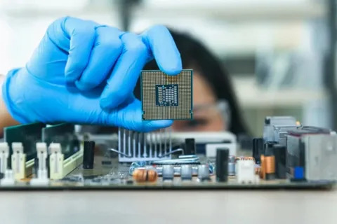
#Infineon Technologies#MemorandumofUnderstanding#supplychains#Semiconductor Assembly and Test#electronicsnews#technologynews
0 notes
Text
Semiconductor Assembly and Testing Services (SATS) Market Growth Driven by AI, IoT, and 5G Technologies
The Semiconductor Assembly and Testing Services (SATS) market is witnessing remarkable growth, driven by the increasing demand for advanced semiconductor packaging and testing solutions. As industries such as artificial intelligence, 5G connectivity, automotive electronics, and the Internet of Things (IoT) expand, the need for efficient and high-performance chips is surging. This has led to the rapid adoption of outsourcing models, where semiconductor manufacturers rely on SATS providers for cost-effective and technologically advanced solutions.
Rising Demand for Advanced Semiconductor Packaging
With the growing complexity of semiconductor designs, traditional packaging methods are no longer sufficient to meet modern performance requirements. Advanced packaging technologies such as fan-out wafer-level packaging (FOWLP), system-in-package (SiP), and 2.5D/3D packaging are gaining traction. These innovations enhance chip functionality while reducing size and power consumption, making them essential for next-generation applications like AI processors and autonomous vehicles. SATS providers are investing heavily in these technologies to remain competitive in the evolving market.
Impact of 5G and IoT on Market Expansion
The global rollout of 5G networks and the proliferation of IoT devices are significant drivers of the SATS market. 5G technology demands high-frequency semiconductor components that require precise assembly and testing. Similarly, IoT applications, from smart homes to industrial automation, rely on efficient and reliable semiconductor solutions. SATS companies are focusing on developing new testing methodologies to ensure these devices meet stringent performance and reliability standards.
Automotive Electronics and the Need for Rigorous Testing
As automotive technology advances, semiconductor components play a crucial role in electric vehicles (EVs), autonomous driving systems, and advanced driver-assistance systems (ADAS). These applications require highly reliable and durable chips that can withstand harsh environmental conditions. SATS providers are enhancing their testing capabilities to address the automotive industry's stringent safety and performance standards. The growing adoption of electric and autonomous vehicles is expected to drive further demand for specialized semiconductor testing services.
Outsourcing Trends and Cost-Effective Solutions
Many semiconductor companies are increasingly outsourcing their assembly and testing processes to SATS providers to optimize costs and streamline production. This trend is particularly prevalent among fabless semiconductor firms that focus on chip design while relying on external partners for manufacturing and testing. Outsourcing enables semiconductor companies to scale operations quickly, access advanced technologies, and reduce capital expenditures, making it a preferred strategy in the industry.
Challenges and Opportunities in the SATS Market
Despite the promising growth of the SATS market, challenges such as supply chain disruptions, rising production costs, and geopolitical uncertainties impact market stability. However, these challenges also create opportunities for innovation and strategic partnerships. Companies that invest in automation, artificial intelligence-driven testing, and sustainable manufacturing practices are likely to gain a competitive edge. Additionally, the shift towards localized semiconductor production in regions like the U.S. and Europe is expected to reshape the global SATS landscape.
Conclusion
The Semiconductor Assembly and Testing Services (SATS) market is at the forefront of technological advancements, driven by increasing demand for high-performance and energy-efficient chips. With continuous innovation in packaging, testing, and automation, SATS providers are playing a crucial role in shaping the semiconductor industry's future. As emerging applications like AI, 5G, and electric vehicles continue to expand, the market is poised for sustained growth, offering significant opportunities for both established players and new entrants.
1 note
·
View note
Text
https://introspectivemarketresearch.com/reports/outsourced-semiconductor-assembly-and-test-services-market/
#Outsourced Semiconductor Assembly and Test Services Market Size#Outsourced Semiconductor Assembly and Test Services Market Share#Outsourced Semiconductor Assembly and Test Services Market Growth#Outsourced Semiconductor Assembly and Test Services Market Trends#Outsourced Semiconductor Assembly and Test Services Market Forecast Analysis#Outsourced Semiconductor Assembly and Test Services Market Segmentation#Outsourced Semiconductor Assembly and Test Services Market 2024#Outsourced Semiconductor Assembly and Test Services Market CAGR#Outsourced Semiconductor Assembly and Test Services Market Analyzer Industry
0 notes
Text
Outsource Semiconductor Assembly and Testing Services (OSAT Services) Market Trends, Growth, Top Companies, Revenue, and Forecast to 2032
Outsource Semiconductor Assembly and Testing Services (OSAT services) have become essential for semiconductor manufacturers aiming to streamline operations and enhance productivity. These services encompass a range of critical functions, including the assembly, packaging, and testing of semiconductor devices, allowing manufacturers to focus on core activities such as design and fabrication. By leveraging the expertise and specialized equipment of OSAT providers, companies can optimize their processes, improve product quality, and reduce time-to-market.
The OSAT sector is experiencing robust growth, driven by increasing demands for sophisticated semiconductor solutions across various industries. As technology advances, devices are becoming more complex, necessitating specialized assembly and testing capabilities. OSAT providers are continuously innovating, offering advanced packaging solutions that meet the performance and reliability requirements of next-generation applications, from consumer electronics to automotive and industrial sectors.
The Outsource Semiconductor Assembly and Testing Services (OSAT services) Market is expanding as semiconductor manufacturers increasingly outsource assembly and testing processes to enhance efficiency, reduce costs, and focus on core competencies amid rising demand for semiconductor products.
Future Scope
The future of OSAT services is promising, with substantial growth anticipated as semiconductor technology continues to evolve. As the industry shifts towards miniaturization and integration, there will be a growing need for advanced packaging solutions that can accommodate high-density designs and complex functionalities. OSAT providers are positioned to play a crucial role in meeting these needs, offering expertise in innovative packaging techniques such as system-in-package (SiP) and 3D packaging.
Moreover, the increasing emphasis on sustainability will influence OSAT services, prompting providers to adopt eco-friendly materials and processes. As manufacturers seek to reduce their environmental impact, OSAT providers will need to innovate in ways that minimize waste and promote recycling within assembly and testing operations. This shift towards sustainability will be essential for compliance with evolving regulations and for meeting consumer expectations for environmentally responsible products.
Trends
Several key trends are shaping the OSAT services market. One significant trend is the increasing adoption of automation in assembly and testing processes. OSAT providers are leveraging advanced robotics and automated systems to enhance efficiency, reduce labor costs, and improve the accuracy of operations. This trend is particularly relevant as manufacturers seek to scale production while maintaining high quality.
Another trend is the growing collaboration between semiconductor manufacturers and OSAT providers. As the semiconductor landscape becomes more competitive, partnerships are forming to leverage complementary strengths in design, assembly, and testing. This collaboration is vital for accelerating product development cycles and ensuring that new technologies are brought to market efficiently.
Application
OSAT services find applications across various sectors, including consumer electronics, automotive, telecommunications, and industrial automation. In consumer electronics, OSAT providers play a critical role in ensuring that devices such as smartphones, tablets, and wearables are assembled and tested to meet rigorous quality standards. This attention to quality is essential for delivering reliable products in a fast-paced market.
In the automotive sector, OSAT services are indispensable for the assembly and testing of semiconductor components used in advanced driver-assistance systems (ADAS), power management, and infotainment systems. The reliability of these components is paramount, as they directly impact vehicle safety and performance.
Telecommunications also relies heavily on OSAT services, with providers ensuring that semiconductor components used in network infrastructure meet stringent performance and reliability standards. As the industry transitions to 5G and beyond, OSAT providers will be instrumental in supporting the development of next-generation communication technologies.
Key Points
Essential for streamlining semiconductor manufacturing operations.
Driven by the increasing complexity of semiconductor devices across industries.
Promising future with growth opportunities in advanced packaging and sustainability.
Trends include automation and collaboration between manufacturers and OSAT providers.
Applied in consumer electronics, automotive, telecommunications, and industrial sectors.
Read More Details: https://www.snsinsider.com/reports/outsourced-semiconductor-assembly-and-test-services-market-4535
Contact Us:
Akash Anand — Head of Business Development & Strategy
Email: [email protected]
Phone: +1–415–230–0044 (US) | +91–7798602273 (IND)
0 notes
Text
Vibrant Gujarat: Tata Group's Bold Move with Semiconductor Plant in Dholera
In a significant stride towards technological advancement and industrial growth. Tata Group, under the leadership of Chairman N Chandrasekaran, has unveiled plans to establish. A state-of-the-art semiconductor fabrication plant in Dholera, Gujarat. This ambitious project, slated to commence operations in 2024. Was officially announced during the 10th Vibrant Gujarat Global Summit, marking. A…

View On WordPress
#tata electronics#Tata group plans for a semiconductor factory in Dholera#Tata group plans for a semiconductor factory in Gujarat#Tata group plans for a semiconductor factory in India#Tata group plans for a semiconductor in india#tata semiconductor assembly and test private limited#tata semiconductor investment#tata semiconductor manufacturing company name#tata semiconductor manufacturing company share price#tata semiconductor manufacturing plant in india#tata semiconductor plant location
0 notes
Text
OSAT companies in mainland China lower chip packaging prices
August 25, 2023 /SemiMedia/ — According to industry insiders, OSAT (Outsourced Semiconductor Assembly and Testing) companies in mainland China are lowering prices to win more orders. The utilization rate of mature wire-bonding and mid-to-high-end flip-chip packaging processes in chip packaging has not yet changed significantly, but OSAT companies in mainland China can provide more substantial…
View On WordPress
#electronic components news#Electronic components supplier#Electronic parts supplier#Semiconductor assembly and testing
0 notes
Text
Launch of STS-80 Columbia


"The Space Shuttle Columbia lifts off from the Kennedy Space Center's (KSC) Launch Pad 39B at 2:55:47 p.m. (EST), November 19, 1996. Onboard are astronauts Kenneth D. Cockrell, mission commander; Kent V. Rominger, pilot; along with Story Musgrave, Tamara E. Jernigan and Thomas D. Jones, all mission specialists. The two primary payloads for STS-80 stowed in Columbia's cargo bay for later deployment and testing are the Wake Shield Facility (WSF-3) and the Orbiting and Retrievable Far and Extreme Ultraviolet Spectrometer (ORFEUS) with its associated Shuttle Pallet Satellite (SPAS)."

Columbia inflight

"This mission patch for mission STS-80 depicts the Space Shuttle Columbia and the two research satellites its crew deployed into the blue field of space. The uppermost satellite is the Orbiting Retrievable Far and Extreme Ultraviolet Spectrograph-Shuttle Pallet Satellite (ORFEUS-SPAS), a telescope aimed at unraveling the life cycles of stars and understanding the gases that drift between them. The lower satellite is the Wake Shield Facility (WSF), flying for the third time. It will use the vacuum of space to create advanced semiconductors for the nation's electronics industry. ORFEUS and WSF are joined by the symbol of the Astronaut Corps, representing the human contribution to scientific progress in space. The two bright blue stars represent the mission's Extravehicular Activities (EVA), final rehearsals for techniques and tools to be used in assembly of the International Space Station (ISS). Surrounding Columbia is a constellation of 16 stars, one for each day of the mission, representing the stellar talents of the ground and flight teams that share the goal of expanding knowledge through a permanent human presence in space."
Date: November 19, 1996
NASA ID: KSC-96PC-1290, KSC-96PC-1292, KSC-96PC-1285, KSC-96PC-1284, KSC-96PC-1292, KSC-96PC-1293, STS080-S-003, KSC-96PC-1288, KSC-96PC-1286, KSC-96PC-1287, MSFC-9611692
#STS-80#Space Shuttle#Space Shuttle Columbia#Columbia#OV-102#Orbiter#NASA#Space Shuttle Program#Launch#LC-39B#Kennedy Space Center#KSC#Florida#November#1996#my post
106 notes
·
View notes
Text

Nature-inspired solar lasers could sustainably power space missions
International scientists, including a team from Heriot-Watt University, has announced plans to develop a revolutionary new way of harvesting solar energy in space.
The new technology would directly convert sunlight into laser beams, facilitating the transmission of power over vast distances, such as between satellites, from satellites to lunar bases, or even back to Earth. The approach is inspired by the way bacteria and other plants and organisms convert light energy into chemical energy—a process known as photosynthesis. Repurposing natural photosynthetic structures from nature will form a key component in the new laser technology.
If successful, their innovative technology could help global space agencies to power future endeavors such as lunar bases or missions to Mars, as well as open new pathways for terrestrial wireless power transmission and sustainable energy solutions globally.
The APACE project brings together researchers from the U.K., Italy, Germany and Poland to create the new type of solar-powered lasers, which will provide reliable, efficient power for the growing number of satellites and future space missions.
The system will repurpose light harvesting antennas of certain photosynthetic bacteria, which are highly efficient at absorbing ambient solar light and channeling its energy to a desired target location as part of their photosynthetic cycle.
The team plans to realize their idea under laboratory conditions first, before testing and refining its suitability for deployment into the space environment.
The researchers will begin by extracting and studying the natural light-harvesting machinery from specific types of bacteria that have evolved to survive in extremely low light conditions. These bacteria have specialized molecular antenna structures that can capture and channel almost every photon of light they receive—making them nature's most efficient solar collectors.
In parallel, the team will develop artificial versions of these structures and new laser materials that can work with both natural and artificial light-harvesters. These components will then be combined into a new type of laser material and tested in increasingly larger systems.
Unlike conventional semiconductor solar panels, which convert sunlight into electricity, their bio-inspired system builds on a sustainable organic platform with the potential for replication in space. It would then allow for the direct distribution of power without relying on an electric intermediary.
Professor Erik Gauger from the Institute of Photonics and Quantum Sciences at Heriot-Watt University is leading the theoretical modeling aspects of the project.
He explains, "Sustainable generation of power in space, without relying on perishable components sent from Earth represents a big challenge. Yet, living organisms are experts at being self-sufficient and harnessing self-assembly. Our project not only takes biological inspiration but goes one step beyond by piggybacking on functionality that already exists in the photosynthetic machinery of bacteria to achieve a breakthrough in space power.
"Our APACE project aims to create a new type of laser powered by sunlight. Regular sunlight is usually too weak to power a laser directly, but these special bacteria are incredibly efficient at collecting and channeling sunlight through their intricately designed light harvesting structures, which can effectively amplify the energy flux from sunlight to the reaction center by several orders of magnitude. Our project will make use of this level of amplification to convert sunlight into a laser beam without relying on electrical components.
"We already know it is possible to grow bacteria in space, for example through studies on the International Space Station. Some tough bacteria have even survived exposure to open space! If our new technology can be built and used on space stations, it could help to generate power locally and even offer a route to sending power to satellites or back to Earth using infrared laser beams.
"This technology has the potential to revolutionize how we power space operations, making exploration more sustainable while also advancing clean energy technology here on Earth. All major space agencies have lunar or Mars missions in their plans and we hope to help power them."
The research team expects to have its first prototype ready for testing within three years.
7 notes
·
View notes
Text
Ratan Tata's Business Strategy

In a strategic move, the Ratan Tata-led Tata Group has partnered with Nasdaq-listed American chip maker Analog Devices (ADI) to explore semiconductor manufacturing opportunities in India. This collaboration, announced last week, marks a significant milestone in India’s push towards self-reliance in semiconductor production.
Tata and ADI’s Major Partnership
Tata Electronics, Tata Motors, and Tejas Networks signed a Memorandum of Understanding (MoU) with Analog Devices to enhance their strategic and business cooperation. The goal of the partnership is to explore the potential for semiconductor manufacturing within India. ADI’s semiconductor products are expected to be utilized across Tata Group’s key applications, including electric vehicles (EVs) and network infrastructure.
This collaboration aligns with India’s ambitions to strengthen its semiconductor industry and make a significant contribution to the global supply chain. The Tata Group had already received approval from the Indian government to establish semiconductor assembly, testing, and fabrication facilities within the nation.
Tata’s $14 billion semiconductor investment
Tata Group, a 156-year-old conglomerate with a diverse business portfolio, has committed a massive $14 billion to establish India’s first semiconductor fabrication plant in Gujarat along with a chip assembly and testing plant in Assam. This investment reflects Tata’s dedication to building a strong domestic semiconductor ecosystem.
The construction of these plants, approved by the government earlier this year, is a key step in reducing India’s dependence on semiconductor imports while positioning the country as a significant player in the global tech industry.Read More-https://voiceofentrepreneur.life/
2 notes
·
View notes
Text
US launches $1.6B bid to outpace Asia in packaging tech
New Post has been published on https://thedigitalinsider.com/us-launches-1-6b-bid-to-outpace-asia-in-packaging-tech/
US launches $1.6B bid to outpace Asia in packaging tech
.pp-multiple-authors-boxes-wrapper display:none; img width:100%;
The US is betting big on the future of semiconductor technology, launching a $1.6 billion competition to revolutionise chip packaging and challenge Asia’s longstanding dominance in the field. On July 9, 2024, the US Department of Commerce unveiled its ambitious plan to turbocharge domestic advanced packaging capabilities, a critical yet often overlooked aspect of semiconductor manufacturing.
This move, part of the Biden-Harris Administration’s CHIPS for America program, comes as the US seeks to revitalise its semiconductor industry and reduce dependence on foreign suppliers. Advanced packaging, a crucial step in semiconductor production, has long been dominated by Asian countries like Taiwan and South Korea. By investing heavily in this area, the US aims to reshape the global semiconductor landscape and position itself at the forefront of next-generation chip technology, marking a significant shift in the industry’s balance of power.
US Secretary of Commerce Gina Raimondo emphasised the importance of this move, stating, “President Biden was clear that we need to build a vibrant domestic semiconductor ecosystem here in the US, and advanced packaging is a huge part of that. Thanks to the Biden-Harris Administration’s commitment to investing in America, the US will have multiple advanced packaging options across the country and push the envelope in new packaging technologies.”
The competition will focus on five key R&D areas: equipment and process integration, power delivery and thermal management, connector technology, chiplets ecosystem, and co-design/electronic design automation. The Department of Commerce anticipates making several awards of approximately $150 million each in federal funding per research area, leveraging additional investments from industry and academia.
This strategic investment comes at a crucial time, as emerging AI applications are pushing the boundaries of current technologies. Advanced packaging allows for improvements in system performance, reduced physical footprint, lower power consumption, and decreased costs – all critical factors in maintaining technological leadership.
The Biden-Harris Administration’s push to revitalise American semiconductor manufacturing comes as the global chip shortage has highlighted the risks of overreliance on foreign suppliers. Asia, particularly Taiwan, currently dominates the advanced packaging market. According to a 2021 report by the Semiconductor Industry Association, the US accounts for only 3% of global packaging, testing, and assembly capacity, while Taiwan holds a 54% share, followed by China at 16%.
Under Secretary of Commerce for Standards and Technology and National Institute of Standards and Technology (NIST) Director Laurie E. Locascio outlined an ambitious vision for the program: “Within a decade, through R&D funded by CHIPS for America, we will create a domestic packaging industry where advanced node chips manufactured in the US and abroad can be packaged within the States and where innovative designs and architectures are enabled through leading-edge packaging capabilities.”
The announcement builds on previous efforts by the CHIPS for America program. In February 2024, the program released its first funding opportunity for the National Advanced Packaging Manufacturing Program (NAPMP), focusing on advanced packaging substrates and substrate materials. That initiative garnered significant interest, with over 100 concept papers submitted from 28 states. On May 22, 2024, eight teams were selected to submit complete applications for funding of up to $100 million each over five years.
According to Laurie, the goal is to create multiple high-volume packaging facilities by the decade’s end and reduce reliance on Asian supply lines that pose a security risk that the US “just can’t accept.” In short, the government is prioritising ensuring America’s leadership in all elements of semiconductor manufacturing, “of which advanced packaging is one of the most exciting and critical areas,” White House spokeswoman Robyn Patterson said.
The latest competition is expected to attract significant interest from the US semiconductor ecosystem and shift that balance. It promises substantial federal funding and the opportunity to shape the future of American chip manufacturing. As the global demand for advanced semiconductors continues to grow, driven by AI, 5G, and other emerging technologies, the stakes for technological leadership have never been higher.
As the US embarks on this ambitious endeavour, the world will see if this $1.6 billion bet can challenge Asia’s stronghold on advanced chip packaging and restore America’s position at the forefront of semiconductor innovation.
(Photo by Braden Collum)
See also: Global semiconductor shortage: How the US plans to close the talent gap
Want to learn more about AI and big data from industry leaders? Check out AI & Big Data Expo taking place in Amsterdam, California, and London. The comprehensive event is co-located with other leading events including Intelligent Automation Conference, BlockX, Digital Transformation Week, and Cyber Security & Cloud Expo.
Explore other upcoming enterprise technology events and webinars powered by TechForge here.
Tags: ai, AI semiconductor, artificial intelligence, chips act, law, legal, Legislation, Politics, semiconductor, usa
#2024#5G#Accounts#Administration#ai#ai & big data expo#AI semiconductor#America#amp#applications#Art#artificial#Artificial Intelligence#Asia#automation#betting#biden#Big Data#billion#Business#challenge#China#chip#chip shortage#chips#chips act#Cloud#Commerce#competition#comprehensive
3 notes
·
View notes
Text
Quantum Sensing Applications Nears Industry Marketing

Commercialisation of Quantum Sensing Applications enables sophisticated atomic-level sensing.
Quantum sensing, which allows sensors to collect atomic-level data, is advancing swiftly and is ready for commercial usage. Quantum sensors are developing enough for pilot programs in many environments and applications. The route to commercialisation may be short, thus decision-makers across industries should familiarise themselves with this technology despite engineering, product development, market access, and ecosystem formation hurdles.
Also see Patero Integrates Post-Quantum Encryption into DUST Platform.
Applications of Quantum Sensing
Traditional sensors are less accurate, consistent, and frequent than quantum sensors. Accuracy is crucial for applications where sensor technology is inadequate. The technology is expected to have a big impact due to the extensive use of sensors and the 14.8 billion (and growing) Internet of Things-connected devices.
Quantum sensing's promise in monitoring, imaging, navigation, and identification will impact many areas. These include:
Life Sciences: single-neuron analysis, clinical magnetoencephalography (MEG), metabolism monitoring, MRI quality improvement, and brain and cardiovascular imaging. Noninvasive brain-computer interfaces should also aid media control and engagement.
Navigation: Production line monitoring, optimisation, and fault detection improve auto and assembly precision. This is done with magnetometers, IMUs, magnetic sensors, and accurate atomic clocks.
Energy and Materials: Exploration of fossil resources, geothermal reservoir monitoring, nuclear energy and waste management, and renewable energy optimisation. Due to high temperatures, conventional sensors cannot detect magnetic fields in fusion reactors, but quantum sensors can.
Facilitating quantum networks, improving electrical grids and distribution, and enabling communications.
Microelectronics: Nanometre precise quantum imaging sensors in semiconductor fabrication.
Quantum sensing simplifies processes, cuts costs, and solves impossible problems, generating new use cases.
A Small but Growing Ecosystem
Despite being smaller than quantum computing, quantum-sensing is slowly developing. Today, there are 48 quantum sensing startups, some founded in the recent two years. That the ecosystem's main pieces, such software and hardware, are prototypes shows its technological maturity.
Over 80% of venture capital and corporate investments in quantum sensing occurred between 2001 and 2023. The majority of revenue comes from components and collaborative research, but hardware development and applications/services receive more investment than players.
New sensor and control technologies are making quantum-sensing devices smaller and more commercially viable. Shielding, sensor-based signal amplification, and AI are employed to solve technical problems such ambient noise.
The four main quantum-sensing technology layers are:
Wire, chips, and sensing devices like superconductors and diamonds comprise the Component Layer.
Layer of Quantum Sensing: Sensor hardware, embedded software for basic processing, and data readouts.
Orchestration Layer: Data platforms and analytics modules to organise sensor data and gain insights.
Application and Services Layer: Diagnoses, prognoses, and prescribes sensor readouts using advanced analytics and AI.
Application software and services become more valuable as hardware progresses, allowing data interchange and sensor combination that may lower user costs and improve accuracy.
Strategic Engagement Brings Potential to Life
Corporate leaders should study and test quantum-sensing use cases early to obtain a competitive edge. We must determine the optimal technology and find high-value problems that quantum sensing can tackle. Current quantum-sensing technologies include solid-state spins, neutral atoms, superconducting circuits, and trapped ions. These devices measure temperature, gravity, and magnetic fields. Quantum sensors are more expensive than traditional ones, but standardisation could enhance their economic case.
Businesses are miniaturising quantum sensors for ultraprecise navigation and diagnostics. Companies considering this technology should:
Assess skills and build teams that prioritise talent, training, and innovation.
Usability design and upskilling prepare non-quantum user groups like medical technicians.
Interpret quantum sensor datasets, which can reach ten gigabytes per second, using AI.
Partnerships are key to connecting lab prototypes to industry applications. Partnerships can improve value chain coverage without one business establishing all competencies.
Leaders should assess their value offerings, ecosystem position, and skill gaps before partnering. The field is changing quickly, therefore partners must adapt. Discuss IP, customer, and data sharing.
Numerous sectors must assess how quantum sensing fits into their goals and whether to commercialise it as its widespread use approaches.
#QuantumSensingApplications#Quantumsensors#quantumcomputing#artificialintelligence#News#Technews#Technology#Technologynews#Technologytrends#Govindhtech
0 notes
Text
0 notes
Text
#Outsourced Semiconductor Assembly and Test Services Market Size#Outsourced Semiconductor Assembly and Test Services Market Share#Outsourced Semiconductor Assembly and Test Services Market Growth#Outsourced Semiconductor Assembly and Test Services Market Trends#Outsourced Semiconductor Assembly and Test Services Market Forecast Analysis#Outsourced Semiconductor Assembly and Test Services Market Segmentation#Outsourced Semiconductor Assembly and Test Services Market 2024#Outsourced Semiconductor Assembly and Test Services Market CAGR#Outsourced Semiconductor Assembly and Test Services Market Analyzer Industry
0 notes
Text
Manufacturing Demands Precision: Metrology Services Market on the Rise

The global metrology services market, valued at US$ 649.6 million in 2020, is projected to surpass US$ 1.1 billion by 2031, expanding at a CAGR of 5.7% from 2021 to 2031. As industries increasingly demand high-precision components and efficient quality control, the role of metrology services—ranging from 3D measurement to calibration and reverse engineering—has become vital in industrial operations.
From automotive to aerospace and semiconductors, modern manufacturing ecosystems are leveraging metrology to ensure accuracy, optimize productivity, and meet international quality standards. The convergence of smart automation and Industry 4.0 technologies has further amplified the importance of precise measurements and data integrity, transforming metrology from a back-end process to a strategic pillar of industrial success.
COVID-19’s Impact and Resurgence of the Sector
Like many other industries, the metrology services market experienced disruptions due to the COVID-19 pandemic, with delayed projects, disrupted supply chains, and halted manufacturing lines. However, the crisis also highlighted the need for remote diagnostics, robotic measurement tools, and on-site metrology services—paving the way for a new era of smart, agile, and technology-driven measurement services.
In the post-pandemic world, businesses are adapting to automated inspection tools and digital platforms, enabling real-time analysis, reduced human error, and seamless remote integration. The crisis, thus, served as a catalyst for accelerated technological transformation across the metrology landscape.
Automotive Sector: The Cornerstone of Growth
One of the most significant growth drivers for the metrology services market is the automotive industry. With modern vehicles incorporating advanced driver-assistance systems (ADAS), infotainment solutions, and stringent safety features, the precision alignment of every component is critical.
Metrology services such as 3D laser scanning, coordinate measuring machines (CMMs), and robotic inspection are extensively deployed in vehicle assembly lines for real-time evaluation, component verification, and prototype validation. These services ensure that automobile components such as doors, panels, seats, and frames meet precise specifications, contributing to safety, functionality, and performance.
Additionally, laser scanners and portable coordinate measuring arms are used for hinge line alignment, pilot plant inspections, and virtual assembly of automotive components—minimizing the need for costly physical prototypes.
Smart Automation, IIoT & Industry 4.0 Integration
The ongoing shift toward Industry 4.0 and 5.0 is reshaping the metrology services market. With manufacturing becoming increasingly digitized and interconnected, in-line inspection systems integrated into automated robots are now capable of providing real-time measurement data analysis, ensuring consistent product quality without halting production lines.
The Industrial Internet of Things (IIoT) has further amplified the role of metrology by enabling obedient metrology systems—smart systems that automatically adapt to inspection needs based on process data. This smart automation significantly reduces production downtimes, improves product traceability, and enhances decision-making capabilities for quality assurance teams.
Rising Significance of CMM and Optical Digitizers
Among the most widely used tools in metrology services are Coordinate Measuring Machines (CMMs) and Optical Digitizers & Scanners (ODS).
CMMs offer unmatched precision in measuring complex geometries and are used in testing, design verification, reverse engineering, and component assembly.
ODS, especially 3D laser scanners, have seen increasing adoption due to their ability to measure difficult geometries with superior accuracy.
The adoption of Gantry, Bridge, Horizontal Arm, and Articulated Arm Machines under the CMM category provides industrial users with versatile options tailored to diverse operational needs.
Energy & Power Generation: An Emerging Growth Area
The energy sector is rapidly emerging as a key end-user of metrology services. From turbine blade inspections in power generation to equipment validation in renewable energy projects, metrology services help optimize asset performance and extend the lifecycle of critical infrastructure.
Service providers are increasingly offering customized solutions tailored to the preventive maintenance needs of the energy industry. By adhering to international project norms and compliance standards, these services also support energy firms in achieving operational excellence.
Opportunities & Challenges Ahead
While the future looks promising, the market does face certain hurdles:
Opportunities:
Rising adoption of cloud-based inspection platforms
Expansion of portable metrology devices for on-site analysis
Integration of AI and machine learning for predictive quality control
Challenges:
Slow commercialization in developing regions
Reluctance to adopt new technology in traditional manufacturing environments
Limited availability of user-friendly metrology software
Despite these challenges, the market is well-positioned for long-term growth, especially as industry players prioritize zero-defect manufacturing, sustainability, and digital transformation.
Regional Insights
Asia Pacific is emerging as the fastest-growing region, driven by:
Accelerated industrialization
Expanding automotive and electronics manufacturing hubs
Government investments in smart manufacturing initiatives
North America and Europe continue to dominate the market due to:
Strong presence of aerospace, defense, and automotive giants
High investment in R&D and quality assurance
Early adoption of automation technologies
Countries like China, India, Germany, and the U.S. are poised to witness significant traction due to their expanding manufacturing bases and evolving compliance landscapes.
Competitive Landscape & Key Players
The global metrology services market is characterized by the presence of several key players competing on innovation, service quality, and cost-effectiveness. Some prominent players include:
KLA Corporation
Hexagon AB
Renishaw PLC
SGS Group
Intertek Group Plc.
Jenoptik
Carl Zeiss AG
Faro Technologies
Sasco Metrology Services
Metrologic Group
These companies are focusing on strategic acquisitions, global expansion, and R&D investments to enhance their metrology portfolios. For instance:
In November 2021, Renishaw partnered with Verisurf Software Inc. to synchronize CMM software.
In June 2021, FARO Technologies acquired HoloBuilder, Inc., bringing photogrammetry-based 3D visualization into their metrology ecosystem.
Conclusion: Precision is the Future
As manufacturing and industrial sectors move toward greater automation, sustainability, and product personalization, the need for high-precision measurement services will only intensify. The metrology services market, backed by cutting-edge tools, digitized workflows, and sector-wide innovations, is poised to become a cornerstone of smart manufacturing.
From automotive safety to energy efficiency, and from aerospace accuracy to medical device compliance, metrology services are becoming indispensable across sectors. Stakeholders who invest in agile, integrated, and future-ready metrology solutions will lead the next wave of industrial transformation.
0 notes
Text
Insulink – Redefining Industrial Packaging as a Leading Vacuum Formed Packaging Parts Manufacturer
In an age where precision, safety, and sustainability drive every industrial process, packaging is no longer just a protective layer—it's a key performance factor. For industries where every component counts, Insulink stands out as a dependable vacuum formed packaging parts manufacturer, offering tailor-made, performance-driven packaging solutions to meet the demands of modern manufacturing.
What Are Vacuum Formed Packaging Parts?
Vacuum forming is a thermoforming process in which a plastic sheet is heated and shaped over a mold using vacuum pressure. This process creates high-strength, lightweight packaging components such as trays, inserts, and enclosures that are shaped precisely to fit the product.
As a specialized vacuum formed packaging parts manufacturer, Insulink delivers packaging that:
Enhances product protection during storage and transport
Supports automation in manufacturing and assembly
Increases visual presentation and shelf readiness
Reduces material waste through reusability and recyclability
Why Choose Insulink?
With years of experience and a client-first approach, Insulink is recognized across India as a reliable partner for industrial packaging solutions. Here's why we lead the space:
🔧 Custom Engineering for Precision Fit
Every product has unique dimensions and needs. Our packaging parts are designed with precision to cradle and protect your product securely—minimizing movement and maximizing safety.
🧪 Material Excellence
We offer a wide range of materials such as PETG, PVC, HIPS, ABS, and ESD-safe polymers, suitable for industries like electronics, pharmaceuticals, and automotive.
🛠️ In-House Tooling & Prototyping
From CAD-based designing to CNC mold development and sample testing, everything is handled under one roof—cutting down lead time and improving accuracy.
⚡ Rapid Turnaround & Scalable Production
Whether you require 500 or 50,000 trays, we deliver quickly with consistent quality, thanks to our optimized manufacturing system.
Our Product Range
Insulink manufactures a variety of vacuum formed packaging parts for different applications:
📦 Product & Component Trays
Used widely in electronics, automotive, and mechanical assembly lines for safe handling and transport of small and delicate parts.
🧬 Medical Packaging Inserts
Sterilized and cleanly designed trays for test kits, lab devices, and surgical items—made with medical-grade plastics.
🛠️ Tool Organizers
Custom compartments and slot designs to hold tools securely, ideal for workshop kits, technician kits, and service stations.
🛍️ Retail & Display Packaging
Clear and branded inserts for improved shelf appeal, ideal for cosmetics, electronics, accessories, and consumer products.
📤 Stackable & Transit Packaging
Trays designed for warehouse and logistics use—stackable, durable, and compatible with automation equipment.
⚙️ ESD Trays (Anti-Static)
Specialized trays designed for safe handling of circuit boards, microchips, and electro-sensitive components.
Industries We Serve
As a top vacuum formed packaging parts manufacturer, Insulink proudly serves:
Electronics & Semiconductor Manufacturers
Medical Device & Healthcare Providers
Automotive Parts Suppliers
Tooling & Mechanical Workshops
Retail Product Manufacturers
Pharmaceutical Labs
Aerospace & Defense Vendors
The Benefits of Vacuum Formed Packaging
✔ Customization
Your product’s size, shape, and sensitivity are all factored into our packaging designs.
✔ Lightweight Durability
Vacuum formed trays are lighter than metal or rigid containers, yet strong enough for multiple reuse cycles.
✔ Automation Ready
Designed to be compatible with robotic pick-and-place systems and conveyor belts—perfect for smart factories.
✔ Cost-Effective
Lower tooling cost compared to injection molding, making vacuum forming ideal for both small and large production runs.
✔ Eco-Friendly Options
We offer recyclable and reusable materials to help businesses meet sustainability targets.
Our Proven Process
Requirement Gathering We analyze your product dimensions, weight, fragility, and end-use.
Design & Prototyping CAD-based models are created and prototyped for testing and feedback.
Material Selection Depending on your application—be it ESD, food-grade, or durable-use—we suggest the most suitable materials.
Tooling & Production Our in-house mold and CNC tooling enables faster batch production with high accuracy.
Quality Assurance Each batch undergoes stringent checks for uniformity, fit, surface quality, and durability.
Timely Delivery We pack and dispatch your orders safely, on time, and with full tracking support.What Our Clients Love
✅ Reliable lead times
✅ Expert technical guidance
✅ Tailored design support
✅ End-to-end service from one provider
✅ Competitive pricing across volumes
✅ Quick reorders and scaling options
Whether you are a startup, OEM, or multinational, Insulink has the expertise to upgrade your packaging solutions without increasing your costs.
Request a Quote Today
Are you ready to switch to smarter, stronger, and sustainable packaging?
Whether your goal is to protect, organize, display, or automate—Insulink is the vacuum formed packaging parts manufacturer that understands your needs and exceeds expectations.
📞 Contact Our Team: +91 9205274027 | +91 7838356129 🌐 Explore More at: www.insulink.co.in 📩 Get a Free Quote or Sample Today
Insulink – Engineering Tomorrow’s Packaging, Today.
0 notes