#SemiconductorSolutions
Explore tagged Tumblr posts
Visit Tumblr Blog
Explore Tumblr blogs with no restrictions, modern design and the best experience.
Last Seen Tumblr Blogs


Fun Fact
In 2020, 44% of users from Denmark used Tumblr daily.
Text
#Anglia#ElectronicsDistribution#WinslowAdaptics#SemiconductorSolutions#ICSockets#ObsolescenceManagement#Prototyping#ElectronicsDesign#ComponentEngineering#UKManufacturing#electronicsnews#technologynews
0 notes
Text
From Smartphones to Satellites: The Rise of Compound Semiconductors

In today’s rapidly advancing electronics landscape, semiconductors form the foundation of nearly every modern innovation—from everyday smartphones to cutting-edge satellites and electric vehicles. While silicon has long been the cornerstone of the semiconductor industry, a new class of materials—compound semiconductors—is stepping into the spotlight, offering unique advantages for high-performance and next-generation applications.
This blog explores the world of compound semiconductors: their types, unique properties, applications, challenges, and their immense potential to shape future technologies.
At Orbit & Skyline, we’re helping to accelerate the adoption of compound semiconductors through our specialized Semiconductor FAB Solutions and Semiconductor Material Supply expertise.
What Are Compound Semiconductors?
Unlike elemental semiconductors such as silicon (Si) and germanium (Ge), compound semiconductors are made by combining two or more elements, typically from groups III, V, II, and VI of the periodic table. This combination unlocks specialized electrical, optical, and thermal properties that pure elements cannot achieve.
Some common examples include:
Gallium Arsenide (GaAs)
Indium Phosphide (InP)
Gallium Nitride (GaN)
Silicon Carbide (SiC)
These materials are categorized based on the groups of their constituent elements:
III-V Compounds (e.g., GaAs, InP, GaN)
II-VI Compounds (e.g., CdTe, ZnSe)
IV-IV Compounds (e.g., SiC)
Types of Compound Semiconductors
Compound semiconductors can be further classified into:
III-V Compounds: Known for their excellent electrical properties and direct band gaps, these materials are widely used in high-frequency electronics and optoelectronics.
II-VI Compounds: Efficient in light absorption and emission, they are often used in solar cells and LEDs.
IV-IV Compounds: SiC stands out for its wide band gap and outstanding thermal conductivity, making it ideal for power electronics.
Ternary and Quaternary Compounds: Materials like Aluminum Gallium Arsenide (AlGaAs) and Indium Gallium Nitride (InGaN) allow engineers to "tune" material properties such as band gaps and lattice constants, thanks to advanced Process Engineering techniques.
Key Properties of Compound Semiconductors
Compound semiconductors bring several key advantages over silicon:
High Electron Mobility: Materials like GaAs enable faster electron movement, supporting high-frequency, high-speed devices.
Wide Band Gaps: Materials such as GaN and SiC can handle higher voltages and temperatures—critical for power and harsh-environment applications.
Direct Band Gaps: Unlike silicon, many compound semiconductors efficiently emit and absorb light, making them ideal for optoelectronics.
High Saturation Velocity: Essential for high-frequency and high-speed applications.
Radiation Resistance: Higher tolerance to radiation makes them suitable for space exploration and nuclear environments.
Superior Thermal Conductivity: Especially in SiC, enabling efficient heat dissipation.
Applications of Compound Semiconductors
Due to their exceptional properties, compound semiconductors are vital in a broad range of industries:
Optoelectronics: GaN-based LEDs, laser diodes, and CdTe solar cells.
High-Frequency Electronics: Key components in 5G infrastructure, satellite communications, radar, and microwave systems.
Power Electronics: GaN and SiC power devices revolutionize electric vehicles, renewable energy systems, and efficient power supplies.
RF and Microwave Devices: Critical for wireless communications and defense systems.
Sensors and Detectors: Deployed in medical imaging, environmental monitoring, and industrial sensing.
Challenges and the Road Ahead
Despite their advantages, compound semiconductors come with challenges:
Higher Production Costs: Crystal growth and processing for compound materials remain more expensive than traditional silicon.
Manufacturing Complexity: Precise control overgrowth processes are essential to minimize defects. Orbit & Skyline supports this precision with Equipment Engineering, Process Engineering, and Tool Hook-Up Services.
Scalability Issues: Meeting the growing demand while maintaining high quality remains a challenge.
However, innovation is rapidly overcoming these barriers. Techniques like Molecular Beam Epitaxy (MBE) and Metal-Organic Chemical Vapor Deposition (MOCVD) are enhancing crystal quality while driving down production costs.
The demand for energy-efficient electronics, 5G connectivity, EVs, and renewable energy solutions is fueling heavy investment into compound semiconductor research—positioning them as a cornerstone of future technological advancements.
Conclusion
Compound semiconductors are no longer just a niche innovation—they are transforming industries and enabling the technologies of tomorrow. Their superior electron mobility, wide band gaps, and direct optical transitions are unlocking capabilities that silicon alone cannot achieve.
At Orbit & Skyline, we are proud to be at the forefront of this revolution. Through our integrated Semiconductor FAB Solutions, Global Field Engineering Services, and Material Supply Expertise, we enable faster, scalable, and more efficient compound semiconductor adoption.
With 15+ years of industry leadership and a global network of 500+ skilled engineers, Orbit & Skyline is your trusted partner for semiconductor innovation.
Ready to take the next step? Connect with us at [email protected] to learn more about how we can power your next breakthrough.
#OrbitAndSkyline#SemiconductorSolutions#FABSolutions#MaterialSupply#EngineeringExcellence#ProcessEngineering#ToolHookUpServices
0 notes
Text
Semiconductor Solutions With GAA Process & 2.5D Packaging
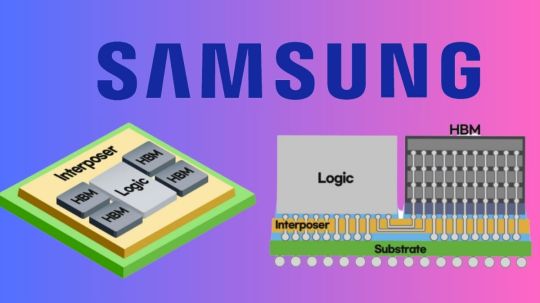
Samsung Electronics will partner with a top Japanese AI startup to develop cutting-edge AI accelerator chips. The company will provide turnkey semiconductor solutions with a 2nm GAA process and 2.5D packaging to preferred networks.
Leading global provider of advanced semiconductor technology, Samsung Electronics, today announced that it will supply Preferred Networks, a top Japanese artificial intelligence company, with turnkey semiconductor solutions utilising the 2-nanometer (nm) foundry process and the cutting-edge 2.5D packaging technology Interposer-Cube S (I-Cube S).
With the help of Samsung’s cutting-edge foundry and cutting-edge packaging goods, Preferred Networks hopes to create potent AI accelerators that will satisfy the constantly rising demand for processing capacity fueled by generative AI.
GAA Process
Samsung has successfully secured orders for the 2nm process with additional improvements in performance and power efficiency, solidifying its position as the industry leader in GAA technology since beginning mass production of the first 3nm process node using Gate-All-Around (GAA) transistor architecture.
With this partnership with Preferred Networks, Japanese firms have achieved a first in the realm of large-scale heterogeneous integrated package technologies, and Samsung intends to intensify its offensive to lead the worldwide advanced package market.
The turnkey solutions include the 2.5D packaging I-Cube S technology, a heterogeneous integration package technology that combines numerous chips into a single package to improve interconnection speed and minimize package space.
In order to achieve an ultra-fine redistribution layer (RDL) and stabilize power integrity for the best possible semiconductor performance, the silicon interposer, or Si-interposer, is essential. The chip was designed by GAONCHIPS, a specialized system semiconductor development business.
According to Junichiro Makino, vice president and chief technology officer (CTO) of computing architecture at Preferred Networks, “This solution will significantly support Preferred Networks’ ongoing efforts to build highly energy-efficient, high-performance computer gear to address generative AI’s expanding computational needs, especially for big language models.”
“This order is crucial because it demonstrates that Samsung’s 2.5D packaging technology and 2nm GAA process technology are the best options for next-generation AI accelerators,” stated Taejon Song, Corporate VP and Head of Samsung Electronics’ Foundry Business Development Team. “It’s are dedicated to working closely with our customers to ensure that our products’ high performance and low power characteristics are fully realized.”
Tokyo-based Preferred Networks vertically integrates the AI value chain from chips to supercomputers and generative AI��foundation models to build cutting-edge hardware and software. It supplies industrial, transportation, healthcare, entertainment, and education products. The company is a global AI leader after topping the Green500 supercomputer list three times in five years.
As a result of their partnership, Samsung and Preferred Networks want to present ground-breaking AI chiplet solutions for the market for generative AI computing and next-generation data centers.
Introduction
With its groundbreaking discoveries, Samsung Electronics leads semiconductor technology’s rapid change. Combining 2.5D packaging technology with Samsung’s latest invention, the 2nm GAA (Gate-All-Around) process, will alter the semiconductor industry by offering Preferred Networks complete semiconductor solutions. This strategic cooperation aims to push semiconductor application performance, efficiency, and scalability.
The Development of Electronic Technology
2nm GAA Process
In the semiconductor industry, the 2nm GAA process represents a major turning point. The limitations of conventional FinFET (Fin Field-Effect Transistor) technology call for a more sophisticated strategy. Better channel management, lower leakage current, and enhanced performance are all made possible by the Gate-All-Around architecture. Samsung plans to use 2nm nodes to reach hitherto unheard-of levels of processing speed, power efficiency, and integration density.
Benefits of the Two-Nm GAA Process
Improved Efficiency: When compared to the earlier 3nm technology, the 2nm GAA process offers up to a 30% performance boost.
Energy Efficiency: It is perfect for applications requiring a longer battery life because it can reduce power usage by up to 50%.
Improved Capabilities: Integrated circuits can now have more transistors per unit area thanks to the 2nm technology.
Inventive 2.5D Packaging Methods
2.5D packaging: what is it?
2.5D packaging technique bridges 2D and 3D packaging. It entails arranging several dies side by side on an interposer, which serves as a high-bandwidth communication channel. Without the complications of complete 3D stacking, this technique lowers latency and improves performance.
Advantages of Two-Sided Packaging
Enhanced Connectivity: Data transfer between chips is made quicker and more effective by the interposer.
Better heat dissipation than 3D packaging in terms of thermal management lowers the possibility of overheating.
Scalability: Promotes the integration of many chip types such as logic and memory on a single package, hence improving functionality.
Semiconductor Solutions
Complete Integration of Samsung’s Turnkey Semiconductor Solutions
The complete semiconductor development process, from design and manufacture to packaging and testing, is covered by Samsung’s turnkey solutions. With a comprehensive package, Samsung guarantees optimal performance and a smooth integration of the finished product.
Customized for favored networks
Samsung’s cutting-edge semiconductor technologies will be extremely beneficial to Preferred Networks, a pioneer in AI and machine learning. High performance and energy efficiency are guaranteed by the partnership’s delivery of specially designed chips that cater to the unique requirements of AI applications.
Principal Elements of Samsung’s Custom Design Services: optimized for a given application by being specifically designed to match its needs.
More Complex Manufacturing Methods: achieving the highest standards of accuracy and productivity by applying cutting-edge procedures.
Thick Validation and Testing: Thorough testing guarantees dependability and functionality in practical uses.
Influence on Machine Learning and Artificial Intelligence
Enhanced Efficiency for Artificial Intelligence Uses
AI and ML application performance is greatly improved by the combination of 2.5D packaging and the 2nm GAA technology. Deep learning models and real-time data analysis depend on quicker processing rates and higher data throughput, which these technologies make possible.
Energy-Secure Edge Computing
Samsung’s solutions offer a substantial advantage in the field of edge computing, where power economy is crucial. The 2nm process’s lower power consumption guarantees longer battery life for edge devices, allowing for more prolonged and demanding computational operations without the need for frequent recharging.
Future Innovations’ Scalability
Scalable and versatile semiconductor solutions are becoming increasingly important as AI and ML applications develop. Samsung’s strategy facilitates the seamless assimilation of novel technology and caters to the increasing needs of forthcoming advancements.
Strategic Alliance with Selected Networks
Combination of Leaders
An innovative and experienced partnership between Preferred Networks and Samsung Electronics is strategic. The alliance uses Preferred Networks’ AI experience and Samsung’s cutting-edge semiconductor technology to provide highly effective, scalable, and reliable AI solutions.
Collaborative Development Programmes
Co-development of application-specific integrated circuits (ASICs) designed specifically for AI workloads is known as custom AI chips.
Improved Software Integration: Making the most of software frameworks to take full advantage of hardware capabilities.
Future Plan: Joint research and development endeavors to maintain a lead in technological breakthroughs.
In conclusion
Samsung Electronics’ 2nm GAA process and 2.5D packaging technology advanced the semiconductor industry. Samsung’s turnkey Preferred Networks solutions will revolutionize AI and ML applications with unprecedented performance, efficiency, and scalability. This strategic collaboration highlights how cutting-edge hardware and creative AI solutions may propel the next wave of technological breakthroughs.
Read more on Govindhtech.com
#govindhtech#News#technologynews#technology#technologytrends#technologysolutions#SAMSUNG#SamsungElectronics#gaaprocess#semiconductor#semiconductorsolutions
0 notes
Text
https://electronicsbuzz.in/renesas-simplifies-software-defined-vehicle-development-with-new-r-car-open-access/
#Renesas Electronics#semiconductorsolutions#RoX#development#SDVs#hardware#operatingsystems#software#automotive#nextgeneration#PowerElectronics#Powersemiconductor#powermanagement
0 notes
Text
Lithography Metrology Equipment Market Expected to Reach $681.4 Million, Globally, by 2026 at 7.2% CAGR: Allied Market Research
The global lithography metrology equipment market size is expected to witness considerable growth, due to emergence of internet of things (IoT) in semiconductor manufacturing and fabrication process. The lithography metrology equipment industry is projected to witness significant growth, especially in the emerging economies such as Asia-Pacific and LAMEA, owing to the development of semiconductor industry in the regions.
Wilmington, Delaware
According to a recent report published by Allied Market Research, titled," Lithography Metrology Equipment Market by Technology, Product, Connectivity, and Application: Global Opportunity Analysis and Industry Forecast, 2018-2026," the global market was valued at $382.6 million in 2018, and is projected to reach $681.4 million by 2026, registering a CAGR of 7.2% from 2019 to 2026.
Download Research Report Sample & TOC: https://www.alliedmarketresearch.com/request-sample/4155
(We look forward to moving quickly to provide the Report Analysis needed for your Business Success) •115 – Tables •85 – Charts •268 – Pages
Lithography is a process in which a pattern from a photomask is transferred to the surface of the wafer. During the lithography process, the wafer gets exposed to ultraviolet laser beam, in which the ultraviolet laser beam passes through photomask layer without a pattern and is irradiated onto photoresist on a wafer. Metrology is essential to control, optimize, and ensure the highest yield in semiconductor manufacturing processes. The lithography metrology equipment has created growth avenues in the semiconductor industry due to its high adoption rates globally.
Prime determinants of growth:
The factors such as high demand for miniaturized electronic devices, increase in trends toward Internet of Things (IoT), growth in the semiconductor industry, problems regarding metrology challenges for complex ICs, and emerging trends toward increase in investment in wafer fabrication equipment and materials are expected to significantly affect the growth of the global lithography metrology equipment market size. These factors are anticipated to either drive or hamper the lithography metrology equipment growth.
Report Coverage and Details:
Aspects
Details
By Technology
CRITICAL DIMENSION SCANNING ELECTRON MICROSCOPE (CD-SEM)
OPTICAL CRITICAL DIMENSION METROLOGY (OCD)
OVERLAY CONTROL
OTHERS
By Product
CHEMICAL CONTROL EQUIPMENT
GAS CONTROL EQUIPMENT
OTHERS
By Process
EDGE
CLOUD
By Application
QUALITY CONTROL & INSPECTION
REVERSE ENGINEERING
VIRTUAL SIMULATION
OTHERS
COVID-19 Scenario:
Metrology and inspection are important for the measurement of the semiconductor manufacturing process. This process is established at critical point of semiconductor manufacturing process to ensure accurate yield. Lithography metrology equipment are used for various factors such as critical dimension measurement, imaging of wafer patterns using photoresist, defect analysis, pattern process development, and material screening. A major restraint, which affects the lithography metrology market is rapid advancement of patterning technology, which increases its overall cost.
Inquiry Before Buying: https://www.alliedmarketresearch.com/purchase-enquiry/4155
Leading Market Players:
The report provides a detailed analysis of these key players of the global lithography metrology equipment market. These players have adopted different strategies such as product development and product launch to increase their market share and maintain dominant shares in different regions. The report is valuable in highlighting business performance, operating segments, product portfolio, and strategic moves of market players to showcase the competitive scenario.
Key Benefits for Stakeholders:
Based on technology, the CD-SEM segment generated the highest revenue in the global lithography metrology equipment market in 2018.
Based on industry, the chemical control equipment segment generated the highest revenue in the lithography metrology equipment market share in 2018.
Based on application, the quality control and inspection segment generated the highest revenue in the lithography metrology equipment market forecast in 2018.
By Region:
Trending Reports in Semiconductor and Electronics Industry (Book Now with Up to 20% Discount + COVID-19 Scenario):
Antenna Market size is projected to reach $40.1 billion by 2032, growing at a CAGR of 9.1% from 2023 to 2032.
Image Sensor Market size is projected to reach $87.5 billion by 2032, growing at a CAGR of 12.9% from 2023 to 2032.
Superconductors Market share is projected to reach $17.4 billion by 2032, growing at a CAGR of 10% from 2023 to 2032.
Power Cable Market size is projected to reach $277.8 billion by 2031, growing at a CAGR of 6.4% from 2022 to 2031
Embedded Systems Market size is projected to reach $163.2 billion by 2031, growing at a CAGR of 6.5% from 2022 to 2031.
About Us:
Allied Market Research (AMR) is a full-service market research and business-consulting wing of Allied Analytics LLP based in Wilmington, Delaware. Allied Market Research provides global enterprises as well as medium and small businesses with unmatched quality of "Market Research Reports Insights" and "Business Intelligence Solutions." AMR has a targeted view to provide business insights and consulting to assist its clients to make strategic business decisions and achieve sustainable growth in their respective market domain.
We are in professional corporate relations with various companies and this helps us in digging out market data that helps us generate accurate research data tables and confirms utmost accuracy in our market forecasting. Allied Market Research CEO Pawan Kumar is instrumental in inspiring and encouraging everyone associated with the company to maintain high quality of data and help clients in every way possible to achieve success. Each and every data presented in the reports published by us is extracted through primary interviews with top officials from leading companies of domain concerned. Our secondary data procurement methodology includes deep online and offline research and discussion with knowledgeable professionals and analysts in the industry.
Contact:
David Correa
1209 Orange Street, Corporation Trust Center, Wilmington, New Castle, Delaware 19801 USA.
Int'l: +1-503-894-6022 Toll Free: +1-800-792-5285
UK: +44-845-528-1300
India (Pune): +91-20-66346060 Fax: +1-800-792-5285 [email protected]
0 notes
Text
Discover Nordson’s stock forecast for 2025–2029, with price targets up to $564.35. Explore its Q2 2025 earnings, Dividend King status, and... #Nordson #NDSN #NDSNstock #stockpriceforecast #DividendKing #precisiondispensing #Atrionacquisition #industrialtechnology #medicalfluidsystems #semiconductorsolutions #stockmarketinvestment
#Atrion acquisition#Best industrial stocks to buy now#Dividend King#Industrial technology#Investment#Investment Insights#Is Nordson stock a good investment#medical fluid systems#NDSN#NDSN stock analysis 2025#Nordson#Nordson Atrion acquisition impact#Nordson Dividend King investment#Nordson Q2 2025 earnings analysis#Nordson stock price forecast 2025–2029#Nordson stock undervalued 2025#Nordson stock.NDSN stock#precision dispensing#Precision dispensing stock investment#Semiconductor equipment stocks 2025#Semiconductor solutions#Stock Forecast#Stock Insights#Stock market investment#Stock Price Forecast
0 notes
Text
Semiconductor Bonding Boom! ⚡ $10.2B Market Projection by 2034 🏭 #Semiconductors #TechGrowth
Semiconductor Bonding is at the forefront of semiconductor assembly and packaging, enabling the production of high-performance computing devices and consumer electronics. This market includes key bonding processes such as wafer bonding, die attach, and wire bonding, which are essential for miniaturization and advanced electronics manufacturing.
To Request Sample Report : https://www.globalinsightservices.com/request-sample/?id=GIS21016 &utm_source=SnehaPatil&utm_medium=Article
The market is experiencing rapid growth, driven by increasing demand for compact and efficient semiconductor devices. Wafer bonding leads the market, playing a crucial role in 3D integration and MEMS applications. Die bonding follows, fueled by the expansion of high-performance computing and automotive electronics. The Asia-Pacific region dominates the market, benefiting from a strong semiconductor manufacturing base and continuous technological innovation. North America ranks second, driven by significant investments in semiconductor research and development. China emerges as the top-performing country due to government-backed initiatives supporting semiconductor advancements, followed by South Korea, home to leading electronics giants.
The market’s expansion is further supported by the rise of IoT, AI, and 5G technologies, which require advanced semiconductor bonding solutions. Miniaturization trends and increased automation in semiconductor production are also contributing to the industry’s strong growth outlook.
Key market segments include die bonding, wire bonding, flip chip bonding, and wafer bonding, with applications spanning consumer electronics, automotive electronics, telecommunications, and medical devices. Cutting-edge bonding technologies such as thermosonic bonding, adhesive bonding, and thermocompression bonding are shaping the future of semiconductor manufacturing.
#semiconductorbonding #waferbonding #dieattach #wirebonding #flipchip #electronicsmanufacturing #highperformancecomputing #automotiveelectronics #iottechnology #5gnetworks #minitech #chipdesign #chipmanufacturing #aiinnovation #techtrends #advancedpackaging #electroniccomponents #digitaltransformation #integratedcircuits #chipmakers #smartdevices #nanotechnology #futuretech #semiconductorsolutions #automation #microelectronics #pcbassembly #innovation #connectivity #telecommunication #nextgentech #smartmanufacturing #sustainabletech #chipindustry #electronicengineering #emergingtech
0 notes
Text
Home appliances are the backbone of #modernliving, simplifying tasks and enhancing our daily routines. From refrigerators to #washingmachines, #semiconductor technology powers your every day #appliances.
But did you know that behind the scenes, high-quality semiconductors play a critical role in ensuring these appliances function reliably and efficiently?
From erratic performance to premature failures, the repercussions of subpar semiconductors are manifold. Imagine investing valuable resources and expertise into crafting cutting-edge appliances, only to have them falter due to inferior semiconductor components. It's a nightmare scenario that manufacturers desperately seek to avoid.
SUV System Ltd is at the forefront of providing cutting-edge #semiconductorsolutions for home appliance manufacturers worldwide. From #voltageregulators to #rectifiers, #diodes to #transistors, our products ensure efficient and reliable performance of the appliances.
At SUV System Ltd, quality isn't just a buzzword – it's a way of life. Rigorous quality control measures, advanced procuring processes, and stringent testing protocols ensure that every #semiconductor leaving our facility meets the highest standards of performance and durability. By prioritizing reliability and longevity, they empower manufacturers to craft appliances that inspire confidence and exceed expectations.
the journey from concept to creation in the #homeappliance industry is fraught with challenges, but with the right semiconductor solutions, manufacturers can turn obstacles into opportunities. Together with SUV System Ltd, let's pave the way for a brighter, more connected future, where quality knows no compromise and #innovation knows no bounds.
For inquiries, assistance feel free to contact us at [email protected] or connect with us on Skype at [email protected]
Or visit us at https://www.suvsystem.com/
1 note
·
View note
Photo

Semiconductor Fabrication Equipment Monitoring | Rugged Monitoring
Semiconductor fabrication equipment monitoring refers to the process of monitoring and maintaining the various machines and tools used to create semiconductor devices. This includes monitoring processes such as lithography, etching, and deposition, as well as the health and performance of the equipment itself.
Read more: https://bit.ly/3DNB9tM
0 notes
Photo

Low Cost & Dependable Manufacturing Semiconductor Solutions
We are providing semiconductor solutions in Israel. The automotive industry with difficult climatic conditions. While consumers demand better features and functionality, on the one hand, laws and regulations are becoming stricter, and raw material prices are rising. It is one of the main reasons automotive and Tier 1 OEMs move from expensive to low-cost centers to build better products at faster speeds and lower costs.
#SemiconductorSolutions#SemiconductorWaferFabrication#SemiconductorPiping#SemiconductorManufacturingMaterials#SemiconductorProcessPiping
0 notes
Text
#Littelfuse#industrial#GateDriver#PowerElectronics#CircuitDesign#SemiconductorSolutions#TechInnovation#Timestech#HighSpeedSwitching#CompactDesign#ElectronicsEngineering#electronicsnews#technologynews
0 notes
Text
#Texas Instruments#automotivechips#AutomotiveInnovation#ADAS#LiDAR#RadarTechnology#BAWClocks#VehicleSafety#AutonomousDriving#SemiconductorSolutions#electronicsnews#technologynews
0 notes
Text
Staying Ahead of Obsolescence: Smart Strategies for the Semiconductor Industry

In the fast-paced world of semiconductor manufacturing, technological advancements are constant—and while that fuels innovation, it also brings a major challenge: obsolescence. As equipment and components rapidly age out of usability, manufacturers face rising costs, production delays, and increased operational risk. Without a clear strategy to manage this, companies may find themselves stuck with outdated systems that drag down performance and profits.
At Orbit & Skyline, we understand that tackling obsolescence isn’t just about replacing old parts—it’s about future-proofing operations. Let’s take a closer look at the core challenges and our proven strategies for managing them.
The Semiconductor Industry’s Obsolescence Challenge
Before solutions come into play, it’s important to understand what makes obsolescence such a pressing issue in the semiconductor sector.
1. Aging Equipment
Many fabrication tools stay in service for decades, even as OEM support phases out. Once that support disappears, spare parts become scarce, maintenance gets complicated, and downtime increases. These legacy systems are still valuable—but keeping them running requires creative, reliable support that OEMs no longer offer.
2. Component Lifecycle Mismatch
While semiconductor tools may last decades, many of their critical subcomponents go end-of-life (EOL) in just a few years. This mismatch can leave manufacturers scrambling to source replacements or redesign systems mid-cycle, all while trying to keep up with demand.
3. Performance and Productivity Drops
As parts become harder to source, tool reliability and performance start to suffer. Failures become frequent, throughput declines, and operational costs spike—ultimately impacting production schedules and customer commitments.
Orbit & Skyline’s Proactive Approach to Obsolescence
At Orbit & Skyline, we believe obsolescence doesn’t have to mean disruption. Our Legacy Tool Management service is built to extend the value of older systems while maintaining cutting-edge performance.
1. Planned Obsolescence Management
We help manufacturers stay ahead by identifying at-risk components before they become production-stoppers. Through predictive analytics, routine assessments, and forward-looking inventory planning, we ensure continuity without the panic.
2. Repair & Refurbishment Programs
Instead of rushing to replace, we rebuild. Orbit & Skyline offers in-house and partnered repair services that breathe new life into aging components. These programs minimize waste, lower costs, and buy time for more permanent upgrades.
3. Retrofits and Continuous Improvements
When tools can’t keep pace, we make them better. Our team retrofits legacy equipment with modern subcomponents, enhancing performance, reliability, and lifespan—without the high cost of full replacement.
4. Expert Knowledge Community
Legacy knowledge is disappearing from the workforce. To bridge that gap, we’ve built a deep bench of legacy system experts who mentor and guide newer engineers. This community ensures continuity of expertise and seamless knowledge transfer across generations.
Why Obsolescence Strategy Matters
Managing obsolescence isn’t optional—it's essential. Companies without a clear plan risk production halt, skyrocketing costs, and falling behind in a competitive market. On the other hand, a structured approach helps manufacturers:
Maintain uptime and throughput
Reduce costs associated with EOL surprises
Extend the value of capital equipment
Navigate industry change with confidence
Orbit & Skyline’s comprehensive strategy brings all these benefits together under one service umbrella.
Future-Proof Your Fab with Orbit & Skyline
As semiconductor technology races forward, the pressure to keep systems current grows stronger. Orbit & Skyline’s Legacy Tool Management gives manufacturers a structured, cost-effective way to manage obsolescence while maintaining productivity and profitability.
With over 15 years of industry expertise and a global team of 500+ engineers, we’re more than just a service provider—we’re your long-term partner in innovation and operational success.
Ready to secure your fab’s future? Explore our Legacy Tool Management services or contact us at [email protected] to learn more.
#ObsolescenceManagement#LegacyToolManagement#EquipmentMaintenance#SemiconductorIndustry#SemiconductorManufacturing#SemiconductorSolutions#FabSolutions
0 notes
Text
Managing Remote Teams in Global Field Engineering: Challenges & Best Practices
In semiconductor manufacturing, field engineering teams often operate across different time zones and geographies. Managing these remote resources efficiently is critical to maintaining smooth operations, minimizing downtime, and delivering consistent results. At Orbit & Skyline, we understand the complexity of this challenge and offer Global Field Engineering services that address both people and process management.
With over 15 years of experience, Orbit & Skyline has earned a reputation for excellence by deploying skilled professionals to semiconductor fabs around the world. Our mission is to deliver high-performance engineering support while ensuring optimal workforce productivity and operational continuity.
Key Challenges & Solutions in Managing Remote Engineering Teams
Managing remote teams in a highly technical industry like semiconductors requires a thoughtful approach to communication, accountability, collaboration, and employee well-being. Here’s how Orbit & Skyline navigates these core challenges:
1. Overcoming Communication Barriers
The Challenge: Time zone differences and the lack of in-person interactions can lead to miscommunications and delays, making it harder for distributed teams to stay on the same page.
Our Solution: We implement a robust, multi-channel communication strategy that includes:
Video conferencing for critical discussions to enhance clarity and engagement.
Instant messaging & collaboration tools for real-time updates.
Emails and structured documentation to preserve key decisions and maintain transparency.
Regular check-ins and team syncs to ensure alignment and inclusion.
These practices foster open communication, build trust, and ensure that every team member feels heard and informed.
2. Ensuring Productivity and Accountability
The Challenge: In remote setups, it can be tough to monitor progress and maintain accountability without direct supervision.
Our Solution: We take a results-driven approach to manage performance through:
Defined KPIs and goal-setting to clarify expectations.
One-on-one meetings and team reviews to monitor progress and provide support.
Project dashboards and tracking tools for real-time visibility.
Regular feedback sessions to recognize achievements and correct course where needed.
This structured framework helps keep our engineers focused, aligned, and motivated.
3. Building Team Cohesion and Culture
The Challenge: Without the informal interactions of a traditional office, remote teams can struggle to build rapport and a unified culture.
Our Solution: We nurture team spirit and cohesion through:
Virtual team-building events like games, brainstorming sessions, and coffee chats.
Inclusive Townhall meetings that celebrate regional diversity and foster connection.
Recognition of milestones and accomplishments to strengthen team bonds.
These initiatives create a strong sense of belonging and shared purpose across our global teams.
4. Promoting Work-Life Balance and Well-Being
The Challenge: Frequent travel and the blurred lines between work and home life can lead to stress or burnout for remote engineers.
Our Solution: We prioritize our employees’ health and well-being through:
3:1 Flexibility – Engineers can take one month off after every three months of on-site service.
Wellness programs – Including virtual fitness sessions and mental health resources.
Encouragement to unplug after hours, promoting healthier boundaries.
By supporting work-life balance, we help our team stay energized, focused, and satisfied in their roles.
Conclusion
Managing remote teams in Global Field Engineering isn't just about logistics—it’s about empowering people, building trust, and fostering a culture of collaboration. At Orbit & Skyline, we’ve built a framework that balances performance with well-being, leveraging our global experience to deliver consistent, high-quality engineering support.
As the semiconductor industry continues to grow, so do our strategies. We remain committed to optimizing our remote team management practices, ensuring our engineers excel—no matter where they are in the world.
0 notes