#Spintronics
Explore tagged Tumblr posts
Visit Tumblr Blog
Explore Tumblr blogs with no restrictions, modern design and the best experience.
Last Seen Tumblr Blogs


Fun Fact
The Tumblr app for Google Glass was released on May 16, 2013.
Text
Misa Explains 1: Spintronics in a nutshell
A series of posts where I will explain bits and pieces of physics I have gathered throughout the my foray into this wonderful science. Warning, these will be long.
Highly inspired by @chemblrish and @minmin-vs-physics 's posts on their fields, check out their posts (linked on this post in various places!)
Wait what even is going on?
Okay, first of all, why are we even talking about spintronics, whatever that means? Now, we live in an age where we need devices, right? Phones, TVs, laptops, name it. All digital devices come under electronics, which is a cluster of what we call "logic devices" (verrry loosely speaking) with various functions, made with expert circuitry to create our sophisticated "smart" devices. Whew. That's a lot of words. But what does it mean? It means that the very device you're using to view this post is made up of very tiny mini devices, which are made to utilize electrical signals (current, flow of electrons) to make it store information, read information, or perform logic tasks ("AND", "OR" "NOT" and the rest. Let me know if you want me to explain those, but this is not the point of the post so I'm letting them hang in the air for now).
We store digital information in the form of 'bits' (I swear all of this is relevant, please be patient) which is a computer's language of storing and using information. If you've watched any show involving hacking, you'll see stacks after stacks of "1"s and "0"s on their high contrast screens in that radioactive green font (general older sister advice: don't use high contrast it hurts your eyes), these are bits and the basis on which logic devices work. Each combination of 1s and 0s makes a different information, which is the backbone of computing. Now, how these devices make 1s and 0s is again a whole course on electronics, so I will skip over it to just preface that they exist and that's how we make digital devices.
All these years, we have used semiconductors, which allow moderate amount of current flow from them (in contrast to conductors, which allow free flow of electrons, and insulators, which do not allow flow of electrons) to make transistors, which are currently the building blocks of circuit-making devices.

[here's a picture containing ICs (the bug-like looking thing covered in wires) which have tiny transistors inside them, and the LEDs, on which the lit ones are "1"s and unlit ones are "0"s. This was my project for one of my courses!]
In electronics, a very famous law called Moore's Law, states that for increase in tech and development, the amount of transistors in integrated circuits (IC) doubles every two years. This moves proportionally with the increase in use of semiconductors, because transistors are made using them.
Every device maker's main goal is to make a device faster, smoother, and more functional. Which means, more transistors, better semiconductors. Moreover, the smaller space occupied by the ICs, the better. But obviously there's a limit to how much we can decrease the size of the transistors. One is the technical issue of creating such a small object, which will require highly precise instruments which we are not in possession of/ not feasible in the long run. The second issue is the working. "Will a semiconductor keep it's properties when they layer is so small?" is a valid question to ask when we go further down in scale. In simple words: in the long run, improving semiconductors for transistors will be difficult. Moore's law plateaus, and the number of transistors doesn't double with two years. What now? We can't just stop developing better computing devices, not just smart devices, astronomy, medicine and other scientific areas also require reliable, stable and fast computing devices.
Which means we desperately need new materials (and techniques) for logic and memory devices.
Hold on, when's spintronics going to start?
Okay background information done. Now we move onto spins and why we use it. We know that atoms are made of protons, electrons and neutrons. Out of these, electrons "revolve" in "orbits" around the nucleus, which holds the protons and neutrons. I put "revolve" and "orbits" in quotes because essentially it's a cloud of probabilities and we have no clue what path it truly takes. Electrons reside in what are called 'orbitals', which are balloon-like spaces which have a high probability of the electrons being present in (@/chemblrish explains orbitals better here).
Now along with the "revolution", electrons also considered to have a "spin". We don't really know if it "spins" the way Bayblades do, but regardless, they have an angular momentum, which is classically something rotating objects possess (@/mimin-vs-physics goes more in depth on quantum mechanical fun stuff) Either way, we don't know why it has angular momentum, but we know it does (at least I have no idea if we've figured it out??). And in true human fashion, we see anything new and think "now how can I utilize this for my benefit?"
Years and years of research later, we figured out something interesting. The angular momentum which the electron spins contain, and the angular momentum of electrons in "orbits" can interact! This interaction is called Spin-Orbit Coupling (SOC) and it causes a bunch of other fascinating phenomena in quantum mechanics. One of which, is that it if we supply electricity into a metal plane, we can align the electrons and their spins in such a way that it causes a stream of current (remember: current is essentially a flow of electrons in one direction) with aligned spins to move into a different layer perpendicularly.
Okay but what does all of this have to do anything with Spintronics?
We're finally at the part where we can discuss what Spintronics is! We can use our now generated spin current to make electronic devices (hence, spintronics!). So, how do we make these tiny devices?
What we first take is a heavy metal (these are metallic elements/alloys with high atomic numbers, which have a lot of free electrons to use) and make a very thin film of it. (The procedure of making thin films is very interesting, and I will make the next post on it!) We can now pass a stream of current/electricity* parallel to the surface of the thin film, which will give us a stream of spin-aligned electrons bouncing to move into an upper layer.
For the upper layer, we add a thin layer of a ferromagnet. A ferromagnet is a type of material which readily aligns its spin on one direction when under a magnetic field (contrary to this are paramagnets which weakly align their spins, and diamagnets which weakly align their spins opposite to the applied field).
Now remember the electrons with their spin aligned which wanted to move into the upper layer? Yeah once they are given an upper layer to move into, they flow into the layer, bringing their aligned spins with them. This spin can now affect the ferromagnet's spin, and align it in either the direction of the applied electric field ( the one applied on the heavy metal layer. I'm marking it as * for you to check which electric field I mean) or directly opposite to the direction of the electric field. This alignment can be measured. The value doesn't matter, only the direction. Is it parallel to the electric field or anti-parallel? "Up" or "down"? "Left" or "right"? Or, in terms of electronics, "1" or "0".
And look! We now have a way to make a tiny device which can display values of "1" or "0"! We used an analog signal (electricity) to create a digital output (1s and 0s)! That is electronics! But because it uses spins, it is called Spintronics.
Because we use Spin-Orbit Coupling, these devices are extremely precise and fast. And the layers of heavy metal/ferromagnet will be in the ranges of nanometers (10^-9 m), so they are also extremely small. We can also choose materials with properties we like (high melting/boiling point, low reactivity) to create devices which can work in extreme conditions (high heat, pressure, reactive areas).
And here we have it! We've made spintronic devices!
End of post disclaimer: I am a Bachelors student and I will have mistakes. I also tend to exaggerate. So if I have made a mistake in this post, please inform me nicely in the comments or tags!
#this took longer than I expected but I was also thown from one deadline to another so-#studyblr#studyinspo#studyspo#physics#aesthetic#academia#studying#study aesthetic#misa's undergrad journey#misa tries#misa explains physics#stem#stemblr#women in stem#spintronics#electronics#I'll keep editing if I find mistakes#but for now this is going out into the wild (internet)
57 notes
·
View notes
Text

Bismuth's mask uncovered: Implications for quantum computing and spintronics materials
Whether bismuth is part of a class of materials highly suitable for quantum computing and spintronics was a long‑standing issue. Kobe University research has now revealed that the true nature of bismuth was masked by its surface, and in doing so uncovered a new phenomenon relevant to all such materials. The team have published their results in a letter in the journal Physical Review B. There is a class of materials that are insulators in their bulk, but robustly conductive at their surface. As this conductivity does not suffer from defects or impurities, such "topological materials," as they are called, are expected to be highly suitable for use in quantum computers, spintronics and other advanced electronic applications.
Read more.
#Materials Science#Science#Bismuth#Spintronics#Quantum computing#Topology#Surfaces#Crystal structure#Kobe University
14 notes
·
View notes
Text
This research is the result of international collaboration involving scientists from the USA, Germany, the UK, the Netherlands, and the Czech Republic. By combining advanced material synthesis, highly sensitive spectroscopy, and complex many-body theory, the team explored the structure of luminous quasiparticles in novel semiconductor magnets. These findings are significant not only for deepening our understanding of magnetic materials but also for driving future technological innovations in this emerging field.
8 notes
·
View notes
Text
Explaining Topological Superconductivity Majorana Fermions
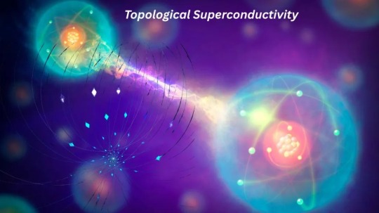
Error-Free, Low-Energy Spintronic Devices Made Possible by Topological Superconductivity
A quantum research breakthrough was the discovery of shielded, non-local transport mediated by edge modes in an iron-based molecule. Topological superconductivity could revolutionise spintronics and quantum computing, according to this study.
Wenyao Liu, Gabriel Natale, and colleagues published “Weyl-Superconductivity revealed by Edge Mode mediated Nonlocal Transport” about their findings. The research examined the iron-based superconductor FeTe₀.₅₅Se₀.₄₅.
Topological superconductivity?
Technically, topological superconductivity is a state of matter with zero resistance and topological properties. Its edge modes or Majorana zero modes are disorder-resistant, non-dissipating electronic states. These Majorana fermions, predicted to exist in topological superconductors, are quasiparticles with half the degrees of freedom of conventional fermions and are their own antiparticles. Topological superconductors have robust, localised edge states within the superconducting gap, unlike ordinary ones.
Key Findings and Method:
The researchers devised a novel technique to prove topological superconductivity through ballistic charge transfer via topologically protected edge states. Ballistic electrons don't scatter. This differs from traditional electrical conduction. Edge mode resonant charge injection and extraction allowed researchers to do this.
Gate-modulated scanning tunnelling spectroscopy and gate-modulated differential conductance were regularly utilised to detect edge modes. These investigations showed how edge modes respond to environmental inputs and relate to material properties.
Superconductivity Signature: The observation and persistence of a zero-bias conductance peak (ZBCP) at zero voltage, strongly associated with the superconducting state up to a critical temperature.
Unique Coexistence: Only when topological, superconducting, and magnetic phases coexisted in the material did a unique conductance plateau appear, defining a parameter space for seeing and manipulating these exotic states.
Non-local Transport: A study showed how these edges coupled drain contacts. After moving the drain contact to the bulk of the material, the transport mechanism became a local Andreev reflection process, which creates an electron and a hole at an interface. This caused edge-specific phenomena and a zero-bias conductance peak.
Robustness and Future Use:
This discovery is important since these edge modes are topologically protected. Before the material's spontaneous magnetisation was significantly reduced, they were unaffected by increasing temperatures or magnetic fields. The robustness of the zero-bias conductance peak to temperature and magnetic field fluctuations supports topological protection.
For practical applications, fault-tolerant quantum computing and spintronics, which processes information using electron spin, require durability. Majorana fermions are intrinsically decoherent-free, making topological superconductors ideal for quantum computer qubits.
The temperature dependence of the zero-bias conductance peak width and the polar Kerr effect, a magnetism-induced shift in reflected light polarisation, revealed more about the material. It implies a sophisticated connection between bulk superconducting properties and topological edge states, deepening our understanding of this unusual form of matter.
Finally
Topological superconductivity in the iron-based FeTe₀.₅₅Se₀.₄₅ has now experimentally shown. This state of matter combines durable, dissipationless edge states (Majorana zero modes) with ordinary superconductivity, as shown by the first observation of shielded, non-local ballistic charge transfer via these modes. Most notably, these edge modes exhibit topological protection irrespective of magnetic fields and temperature. Due to Majorana fermions' natural decoherence defence, topological superconductivity can be used to create fault-tolerant qubits in quantum computers and low-energy, error-free spintronic devices.
#Topologicalsuperconductivity#Majoranazeromodes#Majorana#zerobiasconductancepeak#spintronics#faulttolerantqubits#technology#technews#technologynews#news#technologytrends#govindhtech
0 notes
Video
youtube
(via New form of magnetism could revolutionize spintronics)
0 notes
Text
« Altermagnets consist of magnetic moments that point antiparallel to their neighbours. However, each part of the crystal hosting these tiny moments is rotated with respect to its neighbours. This is like antiferromagnetism with a twist! But this subtle difference has huge ramifications. »
0 notes
Text
Spintronics Market - Forecast(2025 - 2031)
𝐔𝐧𝐥𝐨𝐜𝐤𝐢𝐧𝐠 𝐭𝐡𝐞 𝐏𝐨𝐭𝐞𝐧𝐭𝐢𝐚𝐥 𝐨𝐟 𝐒𝐩𝐢𝐧𝐭𝐫𝐨𝐧𝐢𝐜𝐬: 𝐋𝐚𝐭𝐞𝐬𝐭 𝐌𝐚𝐫𝐤𝐞𝐭 𝐔𝐩𝐝𝐚𝐭𝐞𝐬 | IndustryARC™
Spintronics Market Size is forecast to reach $8200.0 Million by 2030, at a CAGR of 36.2% during forecast period 2024–2030.
👉 𝑫𝒐𝒘𝒏𝒍𝒐𝒂𝒅 𝑺𝒂𝒎𝒑𝒍𝒆 𝑹𝒆𝒑𝒐𝒓𝒕 @
The spintronics market (short for “spin-based electronics”) refers to the industry focused on the development, manufacturing, and application of technologies that utilize the intrinsic spin of electrons, in addition to their charge, for information processing and storage.
𝐊𝐞𝐲 𝐓𝐫𝐞𝐧𝐝𝐬
🔹𝐀𝐝𝐯𝐚𝐧𝐜𝐞𝐦𝐞𝐧𝐭𝐬 𝐢𝐧 𝐒𝐩𝐢𝐧𝐭𝐫𝐨𝐧𝐢𝐜𝐬-𝐛𝐚𝐬𝐞𝐝 𝐌𝐞𝐦𝐨𝐫𝐲:
Technologies like Spin-Transfer Torque Magnetic Random-Access Memory (STT-MRAM) offer faster write speeds and lower power consumption compared to traditional memory technologies.
👉 𝑭𝒐𝒓 𝑴𝒐𝒓𝒆 𝑰𝒏𝒇𝒐𝒓𝒎𝒂𝒕𝒊𝒐𝒏 @
🔹𝐄𝐱𝐩𝐚𝐧𝐬𝐢𝐨𝐧 𝐢𝐧 𝐀𝐮𝐭𝐨𝐦𝐨𝐭𝐢𝐯𝐞 𝐚𝐧𝐝 𝐈𝐧𝐝𝐮𝐬𝐭𝐫𝐢𝐚𝐥 𝐀𝐩𝐩𝐥𝐢𝐜𝐚𝐭𝐢𝐨𝐧𝐬:
Spintronic sensors are increasingly utilized in electric vehicles for battery management systems and in industrial motors and robotics, offering enhanced performance and reliability.
𝐊𝐞𝐲 𝐌𝐚𝐫𝐤𝐞𝐭 𝐃𝐫𝐢𝐯𝐞𝐫𝐬
🔹𝐃𝐚𝐭𝐚 𝐒𝐭𝐨𝐫𝐚𝐠𝐞 𝐃𝐞𝐦𝐚𝐧𝐝:The exponential increase in data generation across industries necessitates more efficient and scalable storage solutions. Spintronic technologies offer high-density, high-speed storage options to meet these growing demands.
🔹𝐄𝐧𝐞𝐫𝐠𝐲 𝐄𝐟𝐟𝐢𝐜𝐢𝐞𝐧𝐜𝐲:
The global emphasis on energy efficiency has led to the adoption of spintronic devices, which consume less power compared to traditional charge-based electronics.
Get this Report on discount of $1000 on purchase of Credit Card
➡️ 𝐤𝐞𝐲 𝐏𝐥𝐚𝐲𝐞𝐫𝐬 : NVE Corporation | Everspin Technologies | Allegro MicroSystems | Synopsys Inc | Avalanche Technology Inc. | IBM | Plures Air | Quantum | Organic Spintronics Srl | Micro-Measurements — Advanced Sensors Technology (Vishay Precision Group) |
#Spintronics#TechnologyTrends#QuantumComputing#MRAM#DataStorage#EnergyEfficiency#Innovation#TechGrowth#SmartDevices#FutureElectronics
0 notes
Text
Study shows robotic third thumb enhances dexterity across diverse users, highlights need for inclusive design

- By Nuadox Crew -
Researchers at the University of Cambridge (UK) demonstrated that the Third Thumb, a robotic prosthetic, can be quickly mastered by a diverse range of people, enhancing manual dexterity.
Their study emphasizes the importance of inclusive design to ensure that new technologies benefit everyone, including marginalized communities.
The Third Thumb, controlled by foot pressure sensors, was tested on 596 participants aged 3 to 96, showing that nearly all could use it effectively within a minute.
Performance varied but showed no gender or handedness bias. The study underscores the need for early-stage inclusivity in developing wearable technologies to ensure accessibility and functionality for a wide range of users.
youtube
Video: "Testing the Third Thumb" by University of Cambridge, YouTube.
Read more at University of Cambridge
Header image credit: Dani Clode Design & The Plasticity Lab.
Scientific paper: Clode, D & Dowdall, L et al. Assessing First Time Usability of a Hand Augmentation Device in a Large Sample of Diverse Users. Science Robotics; 29 May 2024; DOI: 10.1126/scirobotics.adk5183
--
Other recent news:
Spintronics Advancements: Researchers have made a new milestone in spintronics, which could revolutionize electronics by better predicting and controlling spin currents, studying magnetic properties, and temperature effects on materials.
Tandem Solar Cells: Tandem solar cells have achieved over 20% efficiency, marking a significant step forward in solar technology.
NASA’s X-59 Quiet Supersonic Aircraft: NASA’s X-59 quiet supersonic aircraft project has passed a critical milestone, setting the stage for future flight tests.
Lithium Batteries: Korean researchers have developed a revolutionary new lightweight structure for lithium batteries, enhancing ion transport and battery performance.
“Metaholograms”: Scientists have developed a new type of hologram that could transform AR/VR technologies by enabling crosstalk-free, high-fidelity image projection with increased information capacity.
Memristors Mimic Neural Timekeeping: An AI chip breakthrough has occurred with memristors that can mimic the timekeeping of neurons.
#robotics#hand#spintronics#solar energy#energy#nasa#space#x59#lithium#batteries#vr#ar#metaholograms#memristors#ai#semiconductors
0 notes
Text


🐔 or 🥚❓


#filtration#air filter#big tech#technology#tech#spintronics#infrastructure#architecture#cityscape#industrial#development
1 note
·
View note
Text

Currents Control Spiral Spin Structures
The demonstration that helical spin arrangements can be manipulated using electric currents holds promise for spin-based electronics. [...] In so-called spintronic devices, which have applications in communications and computing, information is encoded in patterns formed by electron spins. For efficient device operation, these spin patterns typically need to be manipulated using electric currents. Such electrical control has been demonstrated for certain spin patterns but not for helix-shaped ones, which have potentially useful features including chirality and collective dynamics. Now Je-Geun Park at Seoul National University, South Korea, and his colleagues have achieved electrical control of helical spin patterns and uncovered the mechanism behind this control [1].
Read more.
14 notes
·
View notes
Text
Interestingly, even Edwin Hall, the greatest scientists of all, who discovered the Hall effect, attempted to measure his effect using a beam of light with no success. He summarizes in the closing sentence of his notable paper from 1881: “I think that, if the action of silver had been one tenth as strong as that of iron, the effect would have been detected. No such effect was observed.” (E. Hall, 1881). By tuning in to the right frequency—and knowing where to look—researchers found a way to measure what was once thought invisible.
6 notes
·
View notes
Text

𝐍𝐚𝐧𝐨𝐦𝐚𝐭𝐞𝐫𝐢𝐚𝐥𝐬: Nanoscience focuses on understanding the properties and behavior of nanomaterials, which can exhibit unique properties due to their small size and high surface area.
𝐈𝐧𝐭𝐞𝐫𝐝𝐢𝐬𝐜𝐢𝐩𝐥𝐢𝐧𝐚𝐫𝐲 𝐍𝐚𝐭𝐮𝐫𝐞: Nanoscience and nanotechnology draw from multiple disciplines, including physics, chemistry, biology, engineering, and materials science, to explore phenomena at the nanoscale.
Visit @ https://symbiosisonlinepublishing.com/nanoscience-technology/
#nanoscience#technology#nanosciencetech#nanostructures#nanometerscales#transmissionelectronmicroscopy#nanoscalematerials#nanomedicine#carbondots#nanofabrication#nanolithography#photonics#Macroscope#spintronics#nanomotor#insulintherapy#molecularmachine#nanodevices#journal#journals#pubmed#peerreview#peerreviewed#OpenAccess#openaccessjournal#symbiosisonlinepublishing
1 note
·
View note
Text


Had a great week at Diamond Light Source during my summer studentship.
#student#physics student#physics studyblr#physics#Diamond Light Source#Harwell#Syncatron#PEEM#XMLD#XMCD#Spintronics
1 note
·
View note
Text
Aluminium-20 shatters nuclear norms with explosive triple-proton breakup
Radioactive decay is a fundamental process in nature by which an unstable atomic nucleus loses energy by radiation. Studying nuclear decay modes is crucial for understanding properties of atomic nuclei. In particular, exotic decay modes like proton emission provide essential spectroscopic tools for probing the structure of nuclei far from the valley of stability — the region containing stable…
0 notes
Text
Spintronics Technology: Reshaping the Market Landscape
The spintronics market is projected to reach a value of US$ 687.1 million in 2023, with a forecasted compound annual growth rate (CAGR) of 7.3% leading to a market size of US$ 1,394.2 million by 2033.
The introduction of spintronics technology has revolutionized the storage and processing of massive data, leading to increased market share. Further, the demand for spintronics is driven by its applications in hard drives, digital electronics, sensors, and more.
Spintronics utilizes the spin of electrons rather than their charges, enabling energy-efficient chips and memory-storage devices. Magnetic RAM (MRAM) has emerged as a prominent spintronics technology, offering large storage space and potentially replacing conventional RAMs.
Accelerate Your Success: Unlock the Secrets of the Spintronics Market – Download the Sample Report @ https://www.futuremarketinsights.com/reports/sample/rep-gb-5912
Spintronics enables increased data storage and is considered a rising nanotechnology trend. The adoption of spintronics devices, driven by their superior performance and low power consumption, is predicted to expand the market, particularly in smart devices, IoT, and memory components.
Cost savings in manufacturing and continual research and initiatives are key drivers for market growth. However, challenges such as a lack of awareness among end users and an incomplete understanding of the technology, as well as the need for control over spin from a distance, may restrain the market.
Key Takeaways:
North America holds a 28.9% global share in the spintronics market, driven by its advanced technological infrastructure and strong investment in research and development.
Germany has emerged as a leading player, with government support and prominent companies involved in spintronics technologies.
India, with a CAGR of 10.4%, showcases potential for spintronics adoption, particularly in the automotive industry.
The United Kingdom exhibits a growth trajectory of 8.1% with its innovative startups, research institutions, and spintronic companies driving advancements.
Semiconductor-based spintronics holds a market share of 44.5%, benefiting from advancements in materials and device designs.
Hard disks and MRAMs account for a significant share of 29.8%, enabling high storage densities and improved energy efficiency.
Ask an Analyst @ https://www.futuremarketinsights.com/ask-the-analyst/rep-gb-5912
These trends highlight the global growth and applications of spintronics across various regions and categories.
Competitive Landscape
The spintronics market is distinguished by increasing product penetration, limited product differentiation, and intense rivalry. Also, innovation is critical to gaining a competitive advantage. In recent years, certain important market participants, such as Avalanche Technology and Crocus Technologies, have obtained investment to further their product innovation. As a result, competitive rivalry is intense.
Renesas Electronic Corporation announced the development of circuit technology for an integrated spin-transfer torque magnetoresistive random-access memory (STT-MRAM) test chip with read and write operations produced on a 22-nm process in June 2022.
February 20, 2022 – The spin transport properties of nanoscale graphene-based electrical devices have been enhanced by researchers at the University of Manchester. The National Graphene Institute researchers created an extraordinarily high-quality graphene channel in partnership with Japan and internationally supported students from Ecuador and Mexico, eliminating interference or electronic doping by standard 2D tunnel interactions.
In September 2022, Avalanche Technology announced the availability of new High-Reliability Persistent SRAM (P-SRAM) memory devices manufactured on the 22nm manufacturing technology of UMC. Using Avalanche’s newest Spin Transfer Torque Magnetoresistive RAM technology, the third-generation product platform outperforms previous non-volatile solutions in terms of density, durability, reliability, and power.
Segmentation Analysis of the Spintronics Market
By Device Type:
Semiconductor Based Spintronics
Metallic Based Spintronics
Alloy Based Spintronics
By Application:
Magnetic Sensors
Hard Disks and MRAMs
Electric Vehicles
Quantum Computing
Others
By Region:
North America
Latin America
Europe
East Asia
South Asia
Oceania
The Middle East & Africa
0 notes