#Types of RF Diodes
Explore tagged Tumblr posts
Visit Tumblr Blog
Explore Tumblr blogs with no restrictions, modern design and the best experience.
Last Seen Tumblr Blogs


Fun Fact
Tumblr was created by web developers David Karp and Marco Arment.
Text
What is a Schottky Diode, Types of RF Diodes, hot carrier diode, diode
BAT54SW Series 30 V 600 mA Surface Mount Schottky Barrier Diode - SOT-323
#Diodes Incorporated#BAT54SWQ-7-F#Diodes#Schottky Diodes#Fast switching#manufacturers#RF diode#Schottky barrier diodes#Types of RF Diodes#hot carrier diode#Schottky diode chip#higher switching speed#Schottky diode voltage drop
1 note
·
View note
Text
RF diode, Schottky diode voltage drop, fast switching Types of RF Diodes
NSR0320MW2T1 Series 20 V 50 uA Surface Mount Schottky Barrier Diode - SOD-323
0 notes
Text
https://www.futureelectronics.com/p/semiconductors--discretes--diodes--schottky-diodes/zhcs1000ta-diodes-incorporated-8003485
What is a Schottky Diode, Types of RF diode, higher switching speed
ZHCS1000 Series 1000 mA 40 V 100 uA High Current Schottky Barrier Diode - SOT-23
#Diodes Incorporated#ZHCS1000TA#Diodes#Schottky Diodes#Types of RF diode#higher switching speed#chip#voltage drop#Semiconductor diode#RF Diodes#Schottky barrier diodes#hot carrier diode#Schottky diode manufacturers
1 note
·
View note
Text
https://www.futureelectronics.com/p/semiconductors--discretes--diodes--schottky-diodes/bat54sw-7-f-diodes-incorporated-4009812
Diodes Incorporated, BAT54SW-7-F, Diodes, Schottky Diodes
BAT54SW Series 30 V 600 mA Surface Mount Schottky Barrier Diode - SOT-323
#Diodes Incorporated#BAT54SW-7-F#Diodes#Schottky Diodes#Schottky diode voltage drop#hot carrier diode#RF Diodes#Schottky diode chip#higher switching speed Schottky barrier diodes#manufacturers#Types of RF diode#switching#Semiconductor diode
1 note
·
View note
Text
AM-Detection -the not easy way
Sometimes quite simple things can be a real nightmare if you take a closer look. One of those is AM detection. Your worst enemies are distortion and fading (the latter results in the first). The AM-Detector is only one little part in a receiver, exactly that kind of part usually no one thinks about. "It works, so what should be wrong with?" -a lot and sometimes there's more wrong than right.
A good part of that distinctive AM-Sound we all know is because of the Detector, even under the best conditions. If you're listen to shortwave or the broadcast band during the night then you also have to cope with Fading. Shouldn't be that problem, the automatic gain control takes care of that, right? Ehmmm... Yes. Sometimes. Why the sound gets so distorted when the signal goes down? Just because it's very often 'Selective Fading' and not just Fading -and your Detector doesn't like it.
Really good AM-Reception has a lot in common with High-End-Audio: if it shall work well EVERYTHING has to be well. So let's just talk a bit about Detectors...
Basically the Detector just splits the Audio Signal from the received and amplified Signal. Sounds easy and in fact it is -up to some degree. If you want more than this things getting complicated -really complicated. In at least 999 out of 1000 AM-Receivers for the Detector a small circuitry called 'Envelope Detector' is used, it's just a small Diode (Tube or Semiconductor), a few Resistors and small Capacitors. So, from the view of the Development Engineer: just put half a dozen cheap Components together and Bob's your Uncle. To tell the Truth: compared to the expense that thingy works surprisingly well. Because of this it's the 'Gold Standart' for this task since at least the mid 30s. But as good as it is, it absolutely has it's Limitations. Up to about 15...30% Distortion at a 100% Modulation Level is one, the inability to detect a signal with different sidebands (>selective Fading!) properly another.
To overcome these Limitations a thing named 'Synchronous Detector' was developed many Decades ago. This kind of Circuit has many advantages over the Envelope Detector, but to make one the complexity and the component count of those is just hilarious compared to the Envelope Detector. If only the result counts and nothing else: that's the way to go. We'll talking later how this exactly works, but before this you have to know that in a receiver with a Synchronous Detector also an Envelope Detector is needed: just for tuning in. So first we'll have a closer look how we can get the most ideal Envelope Detector.
Basically it's quite simple: want to have low overall Distortion? Feed it with at least 'a few' volts RF at it's input for having a high ratio between the input voltage and the 'forward voltage' of the Diode. Want low Distortion at low modulation levels? Use a Diode with low Impedance and a load Resistor with a value as low as possible. Want low Distortion at high modulation levels? Just make the input Impedance of the following Stage as high as possible for having the highest possible Ratio between the Resistance of the Load Resistor and the input Impedance of the following Stage.

The Receiver i wanted to use (R+S EK07) has an IF output, meant for exactly such things, the IF Level there's about 250mVpp @ 300kHz. So having everything above in mind -and just adding a 700mVpp IF output for the Synchronous Detector and an additional AGC-Circuitry, then we're coming to this:

The EK07 is a fully tube equipped receiver, so i also want to use tubes as far as possible and -like in the EK07- in a way which guarantees 10k's of Service hours. If at one point a Semiconductor may perform muuuch better -ok, so then. First of all i want high performance. So what tubes may perform optimal here?
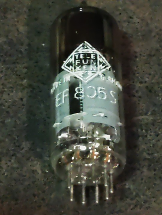
For the first IF-Amp (IF1) not much is needed, the Gain is only about 3, the output voltage low and besides that it has to be an remote-controlled type. Selectivity isn't needed or desired, so no IF-Can, only a Broad-Band setup. Nearly every IF-Tube with a Transconductance of at least about 3000mhos (3mA/V) would do that job. To have better performance i took the EF805s, which is a Special Quality Version of the EF85 -or 6BY7.
Transconductance is about twice what's needed, so we'll have Gain to spare, anyway, it's getting controlled with the AGC so it will work with less current which adds greatly to the service life. So no problems here.
For the second IF-Amp (IF2), things aren't exactly that easy. First: the output for the Synchronous Detector is placed between both Amps and has to deliver a constant voltage, so for the 2nd IF we need an Amplifier with an fixed Gain. A STABLE fixed Gain over long time periods. Further we want to have a relatively high and undistorted output voltage which calls for quite a bit of gain. Wait: there was also that thing with the low-value Load Resistor in the detector itself -so we also need a quite reasonable amount of output power from this stage. In Addition we want to have a stable gain for a time as long as possible. A IF-Tube like the EF805s could also handle this, but then we have to 'beat the crap' out of this thing. Not a good start for a long and stable service life, also not with Special Quality Tubes.
Because of all that my choice was a kinda 'special'-Special-Quality type: the E81L.

The datasheet calls this a 'Long range, Special Quality Tube for the use in Telephone Equipment'. Telephone Equipment? Like an answering machine?? Nope, by far not. Back in these days telephone companies needed to have Amplifiers for pushing the calls through loooong cables for long range service. But: this was all multiplex service, so they pushed dozens and dozens of calls simultaneously through one pair of wires or a Coax. The same way like for cable TV. THIS was these bulbs were meant for. For this task every company employed tens of thousands of such tubes 24/7/365. If a single one failed -most likely somewhere in nowhere of course- they had a problem. So they absolutely had to last.
These little bulbs are designed for about 4.5W plate dissipation at 20mA, the Transconductance is 11000mhos (11mA/V)-so it's about twice an usual IF Tube in every respect. So that's exactly what's needed here: a tube especially designed to last, quite powerful, so we can drive it with comfortable low settings, enhancing service life and stability much further.
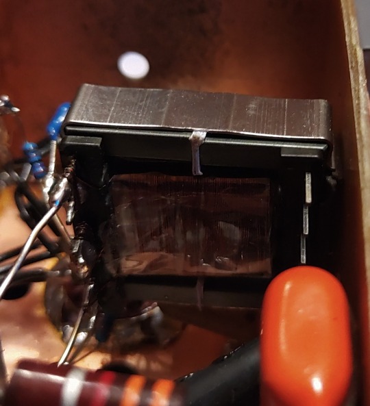
Because we need some amount of power the usual Broad-Band Amplifier arrangement (still: selectivity is not wanted or desired) with just a plate Resistor isn't good here, a suitable inductor works way better here. This has the further advantage that we can build it with a Tab like an Autotransformer -we don't need that much voltage it could deliver with that inductor by far, so this adds further to a good SNR and lower output Impedance. 300kHz trough a transformer? Yep, no problem. Just use the right core. Here it's not a laminated iron core but a ferrite one instead. Cause it's a single-A Amplifier of course we must add an air-gap, preventing saturation.
In a penthode stage the gain depends nearly exclusively on the Transconductance of the tube used, have to much just cut it down. The E81L has a quite high transconductance, about 3 times more than needed -and in the same order than big output tubes like the 6550, EL34 or 6CA7. For cutting that down to the desired level just put a Resistor or Pot in series to the bypass cap of the cathode Resistor. This acts as an series feedback so it also enhances linearity and long time stability greatly. Yap, i thought quite a while about which tube i should use here.
So after all Amplification is done now, we need a Diode for the Envelope Detector. Back in the Octal-Days this was the 6H6 / EB34, later in the Miniature-Days the 6AL5 / EAA91, both with two separate diodes in one bottle (or Can for the 6H6). These were not A DIODE, these were THE DIODE, so there's not much to choose from. Both are kinda close to each other, but are these ideal for what we want? They both can handle a reverse voltage of several hundreds of volts, so waaaay more than we need here. Both having a Plate Resistance of 600-something Ohms per System which is quite low -could be lower, even with both Systems in parallel. Of course these would be work well, no doubt about. But still.... Hey, this should be High-end so we're whining here at a very high level!
Basically we can use EVERY TUBE as a diode: just take the control grid as Anode, the Cathode as what it is and everything else as Shielding. We don't need hundreds of Volts reverse Voltage, nor high current, so also no big Cathode. We only want to have an internal Resistance as low as possible, so a close spacing between the Grid and the Cathode. This calls for a small Tube with a high Gm (or Transconductance) -like the 6AK5 / EF95. Can it handle the reverse voltage we need? Datasheet says 50V, so at least twice of what's needed. So just take one, put some current trough and take the voltage drop. Result: 210 ohms -way less than that what one of the double-diodes would provide, even with both Systems in parallel. Fits very well!

This is the soviet-military version of the 6AK5W / E95F. Special Quality. See these 'trenches' in the bulb? And the microscopic rivets holding the Plate together? The Soviets literally ruggedized the heck out of this tube! Why? Just because they used it widely in their Fighter Planes, ICBM's, Tanks and so on. Doubts about the soviet built quality? Hey, they wanted to win WWIII with them -so: nope. If you ever saw a ruggedized tube: this it is.
After the Detector itself is done, we come to last part of our little contraption: the buffer Amplifier. At the output of the Detector we have the AF as well with the overlayed AGC-Voltage and we want to have an input Impedance as high as possible for the Buffer Amp. Voltage Gain isn't needed -we have plenty of both from the Detector- so we just can use a Cathode Follower for the buffer. Ideally the Buffer should handle both voltages simultaneously, but then the output will be negative with respect to Ground. How to....? Simple: just put that thing between a positive and a negative supply rail. Then the output can swing freely between every positive or negative Potential as desired. Further: we don't need a Grid Resistor! The Grid just follows any voltage swing of the Detector, this also adds to a high input Impedance.
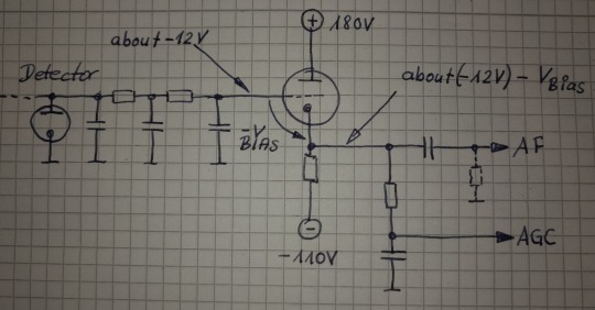
This Circuit will provide us a very high input Impedance, but this is High-End! So: what tube will be the best for? Because of the lack of any Grid Resistor the input Impedance depends now largely on the contact potential of the grid. So we want a tube with low contact potential which calls for a tube with a low Transconductance. Further we want a tube which needs only a low bias voltage for it's Grid, 'cause we'll loose any bias-volt in our AGC-Output voltage. This calls for a tube with an high Gain. Low contact potential and low Transconductance? High Gain?? That's the 12AX7 / ECC83! Ok, it's of course a double Triode, but we still can use the second system for something else -like for the Line-Output Amp. In that Stage there's not much needed so it also will perform well enough there -we're still talking about AM!
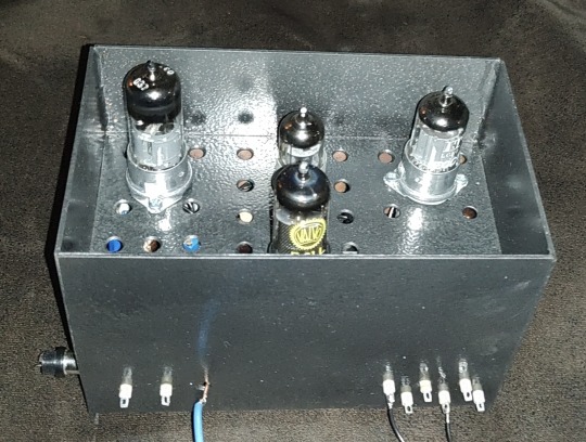
So let's put everything neatly together, adding adequate shielding and so on -and we get this:
So now it's time to have a closer look we did everything right. Just put a 300kHz-Carrier in, 100% modulated with a triangle-signal. We should get a perfect Triangle at the AF-Output -if physics are with us. Due to the Triangle Signal any Distortion can easily be spotted on the Scope.
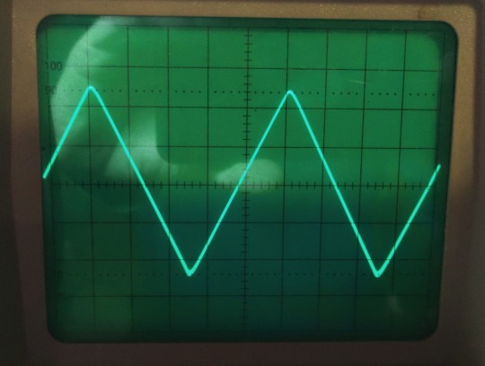
Looks promising! But somehow... Is the beam defocused? Let's take a very close look:

No, it's not. Those are just the very small remnants of the Carrier, so we actually have a look how the Detector works on a nearly 'microscopic' Level. I could take a measurement how much distortion we have left, but the Flanks of the Triangle are perfectly straight, so the Distortion will be really small -like 1% or so worst case. At least for the moment it's not worth the Effort. Compared to the usual 15...30% Distortion at a 100%-Modulation level this works really well, there's no doubt about.
So finally: we wanted to have a Envelope-Detector as good as possible and here we are. Ok, tbh it's better than needed, cause finally the REAL Detector will be a synchronous one. So why i took this that far? Easy: because of mental peace. Now i never have to think about if that part of the whole final thing could work better. As i said before: it's High-End.
Will update you if the next module is ready. But i fear this here was just the more easy part of the whole thing. From now on things may get a bit more tricky...
3 notes
·
View notes
Text
High Linearity Radio Frequency Switches Market - Trends, Growth, including COVID19 Impact, Forecast
High Linearity Radio Frequency Switches Market, Trends, Business Strategies 2025-2032
The global High Linearity Radio Frequency Switches Market size was valued at US$ 456 million in 2024 and is projected to reach US$ 934 million by 2032, at a CAGR of 10.9% during the forecast period 2025-2032. While North America currently dominates with a 38% market share, Asia-Pacific is expected to witness the fastest growth due to increasing 5G deployments.
High linearity RF switches are critical components in modern wireless communication systems, designed to minimize signal distortion while routing high-frequency signals. The High Linearity Radio Frequency Switches market plays a vital role in enabling the coexistence of multiple wireless technologies (such as Wi-Fi 6 and 5G cellular networks) by reducing interference in adjacent frequency bands. The market comprises two primary types: electromechanical switches known for their high power handling and solid-state switches preferred for their compact size and faster switching speeds.
The High Linearity Radio Frequency Switches market growth is primarily driven by escalating demand for high-performance RF components in 5G infrastructure, which requires switches with exceptional linearity to maintain signal integrity. Furthermore, emerging applications in aerospace and defense systems are creating new opportunities, with the aerospace segment projected to grow at 8.2% CAGR through 2032. The High Linearity Radio Frequency Switches market forecast 2025 suggests strong expansion due to increasing investments in 5G, IoT, and satellite communication.
Key High Linearity Radio Frequency Switches market companies, including Qorvo, Skyworks Solutions, and Analog Devices, are actively developing advanced switch solutions to address these evolving requirements. These High Linearity Radio Frequency Switches manufacturers market share leaders have recently launched products featuring improved insertion loss and power handling capabilities. The semiconductor High Linearity Radio Frequency Switches market is further boosted by the rising demand in aerospace, defense, and telecommunications.
Additionally, factors such as the High Linearity Radio Frequency Switches market price, innovations in solar High Linearity Radio Frequency Switches market applications, and opportunities in the High Linearity Radio Frequency Switches reclaim market are shaping future industry dynamics. Overall, the High Linearity Radio Frequency Switches market size, market trends, and adoption across various sectors highlight its growing significance in next-generation wireless systems.
Our comprehensive Market report is ready with the latest trends, growth opportunities, and strategic analysis. https://semiconductorinsight.com/download-sample-report/?product_id=108139
Segment Analysis:
By Type
Solid-State Switches Segment Leads the Market Owing to Superior Performance in High-Frequency Applications
The market is segmented based on type into:
Electromechanical RF switches
Subtypes: Coaxial relays, waveguide switches
Solid-state RF switches
Subtypes: PIN diode switches, GaAs switches, MEMS switches
Hybrid RF switches
By Application
Communication Applications Dominate Market Share Due to 5G Network Expansion
The market is segmented based on application into:
Communication systems
Aerospace and defense
Medical equipment
Test and measurement instruments
Others
By Frequency Range
6-18 GHz Segment Shows Strong Growth Potential for Satellite Communication Applications
The market is segmented based on frequency range into:
DC to 6 GHz
6-18 GHz
18-40 GHz
Above 40 GHz
By End-User
Telecom Infrastructure Providers Lead Market Adoption Due to 5G Deployment
The market is segmented based on end-user into:
Telecom infrastructure providers
Defense contractors
Electronics manufacturers
Research institutions
Regional Analysis: High Linearity Radio Frequency Switches Market
North America The North American market leads in high linearity RF switch adoption due to strong demand from aerospace, defense, and advanced communication sectors. The U.S. accounts for over 80% of regional revenue, driven by substantial investments in 5G infrastructure and next-generation radar systems. Major players like Skyworks Solutions and Qorvo dominate the supply chain, leveraging their technological expertise in GaAs and SOI-based RF switch designs. While the market is mature, ongoing military modernization programs and commercial 5G deployments continue to create opportunities for high-performance RF switching solutions.
Europe Europe maintains a strong position in the high linearity RF switch market, supported by robust industrial standards and innovation in automotive radar applications. Germany and the UK are key markets, hosting leading semiconductor manufacturers including Infineon Technologies. Strict EMC regulations and growing adoption of IoT devices are accelerating demand for interference-resistant RF switching solutions, particularly in the 24-80 GHz frequency bands. However, the market faces challenges from economic uncertainties and competition from Asian manufacturers offering cost-competitive alternatives.
Asia-Pacific The Asia-Pacific region is experiencing the fastest growth in high linearity RF switch adoption, with China accounting for nearly 50% of regional demand. Rapid 5G network expansion, coupled with government initiatives like China’s “New Infrastructure” project, is driving substantial investments in RF components. Japan and South Korea remain technology leaders in miniaturized RF switch designs, while emerging markets such as India present opportunities due to expanding telecommunications infrastructure. Cost pressures remain intense in the region, prompting suppliers to optimize production efficiency while maintaining signal integrity specifications.
South America South America’s high linearity RF switch market is developing gradually, with Brazil representing the largest potential market. Limited local manufacturing capacity creates heavy dependence on imports, though recent economic stabilization is encouraging telecommunications infrastructure upgrades. The region’s focus remains primarily on cost-effective solutions for commercial applications, with specialized high-performance RF switching mainly confined to military and satellite communication systems. Currency volatility and regulatory inconsistencies continue to restrain more robust market growth.
Middle East & Africa The MEA region is witnessing increasing demand for high linearity RF switches, driven by smart city initiatives in the Gulf Cooperation Council countries and expanding mobile networks across Africa. The United Arab Emirates and Saudi Arabia are investing heavily in 5G and aerospace applications, creating opportunities for high-end RF components. However, technical sophistication requirements and limited local technical expertise pose challenges for market penetration. Infrastructure development in Sub-Saharan Africa remains constrained by funding limitations, prioritizing basic connectivity solutions over premium RF components.
List of Leading High Linearity RF Switch Manufacturers
PSemi (U.S.)
Renesas Electronics Corporation (Japan)
Analog Devices, Inc (U.S.)
Skyworks Solutions Inc (U.S.)
MACOM Technology Solutions (U.S.)
Nisshinbo Micro Devices Inc (Japan)
Qorvo (U.S.)
JFW Industries (U.S.)
Microwave Photonic Systems, Inc (U.S.)
QuinStar Technology, Inc (U.S.)
Infineon Technology (Germany)
The global rollout of 5G infrastructure is creating significant demand for high linearity radio frequency switches. These components are critical for managing signal routing in base stations and mobile devices, where multiple frequency bands must coexist without interference. With telecom operators investing approximately $200 billion annually in 5G deployments worldwide, the market for supporting RF components is experiencing robust growth. High linearity switches enable better signal integrity and lower insertion loss, which are essential for maintaining 5G network performance in dense urban environments and high-frequency millimeter wave applications.
Modern wireless devices now incorporate multiple radios (cellular, Wi-Fi, Bluetooth, GPS) that must operate concurrently, creating substantial demand for advanced RF switching solutions. The average smartphone today contains 30-40 RF switches, compared to just 10-15 devices a decade ago. This exponential growth in RF content per device, combined with annual smartphone shipments exceeding 1.2 billion units globally, creates a substantial and growing market for high performance switching components. Recent advancements in switch linearity (IP3 figures exceeding +70 dBm) are enabling device manufacturers to meet increasingly stringent coexistence specifications while reducing power consumption.
Defense modernization programs worldwide are creating opportunities for high reliability RF switches in radar, electronic warfare, and satellite communication systems. The global defense electronics market, valued at over $150 billion, is increasingly adopting solid-state switches with MIL-STD-883 compliance for their superior linearity and switching speed compared to electromechanical alternatives. Modern phased array radar systems may incorporate hundreds of high linearity switches per array, while next-generation satellite constellations are driving demand for radiation-hardened switching solutions capable of operating in harsh environments.
The rapid development of connected vehicle technologies presents significant opportunities for high linearity RF switches. Modern automobiles now incorporate multiple wireless systems including cellular V2X, GPS, satellite radio, and multiple Wi-Fi/Bluetooth connections. Electric vehicles with autonomous driving capabilities are expected to require even more sophisticated RF switching solutions to manage this growing complexity. With over 80 million vehicles produced annually worldwide, the automotive sector represents a substantial expansion opportunity for switch manufacturers who can meet the industry’s rigorous quality and reliability standards.
Emerging artificial intelligence applications in RF system management are creating demand for intelligent switching solutions. AI algorithms can optimize signal paths in real-time based on network conditions, requiring switches that can respond dynamically while maintaining linearity. This evolution from passive to smart RF front ends is driving innovation in digitally controlled switch architectures, with several leading manufacturers already introducing products featuring integrated control logic and programmable performance parameters. The combination of high linearity switching with AI-driven optimization promises significant improvements in spectral efficiency and power consumption.
The rapid development of LEO and MEO satellite constellations for global broadband connectivity is creating robust demand for space-qualified RF switching solutions. Each satellite in these constellations may require dozens of high linearity switches for beamforming and signal routing applications. With thousands of satellites planned for deployment in the coming years, this vertical represents one of the fastest growing segments for specialist RF component manufacturers. The space market also offers attractive margins compared to commoditized consumer applications, though it requires substantial investment in reliability engineering and radiation-hardened technologies.
The market is highly fragmented, with a mix of global and regional players competing for market share. To Learn More About the Global Trends Impacting the Future of Top 10 Companies https://semiconductorinsight.com/download-sample-report/?product_id=108139
Key Questions Answered by the High Linearity Radio Frequency Switches Market Report:
What is the current market size of Global High Linearity Radio Frequency Switches Market?
Which key companies operate in Global High Linearity Radio Frequency Switches Market?
What are the key growth drivers?
Which region dominates the market?
What are the emerging trends?
Browse More Reports:
CONTACT US:
City vista, 203A, Fountain Road, Ashoka Nagar, Kharadi, Pune, Maharashtra 411014
[+91 8087992013]
0 notes
Text
AlGaAs Epitaxial Wafer Market, Trends, Business Strategies 2025-2032
Global AlGaAs Epitaxial Wafer Market size was valued at US$ 1.12 billion in 2024 and is projected to reach US$ 1.56 billion by 2032, at a CAGR of 4.2% during the forecast period 2025-2032.
AlGaAs (Aluminum Gallium Arsenide) epitaxial wafers are semiconductor materials widely used in optoelectronic and radio frequency (RF) applications. These wafers are fabricated by depositing thin layers of AlGaAs on GaAs substrates using epitaxial growth techniques like molecular beam epitaxy (MBE) or metal-organic chemical vapor deposition (MOCVD). Their unique properties, such as high electron mobility and direct bandgap, make them essential for manufacturing LEDs, laser diodes, and high-frequency transistors.
The market is driven by increasing demand for optoelectronic devices in telecommunications, data centers, and consumer electronics. Additionally, advancements in 5G infrastructure are fueling the adoption of AlGaAs wafers for RF applications. However, supply chain disruptions and the rising cost of raw materials pose challenges. Key players like IQE Corporate and II-VI Incorporated are investing in R&D to enhance wafer performance, while the Asia-Pacific region dominates production due to strong semiconductor manufacturing capabilities.
Get Full Report with trend analysis, growth forecasts, and Future strategies : https://semiconductorinsight.com/report/algaas-epitaxial-wafer-market/
Segment Analysis:
By Type
6 Inch Wafers Dominate the Market Due to High Demand in High-Performance Optoelectronics
The market is segmented based on type into:
2 Inch
3 Inch
4 Inch
6 Inch
Others
By Application
Optoelectronic Devices Segment Leads with Widespread Use in LED and Laser Technologies
The market is segmented based on application into:
RF Field
Optoelectronic Devices
Others
By End User
Semiconductor Manufacturers Account for Major Adoption of AlGaAs Epitaxial Wafers
The market is segmented based on end user into:
LED Manufacturers
Semiconductor Fabrication Plants
Research Institutions
Telecommunication Equipment Producers
Regional Analysis: AlGaAs Epitaxial Wafer Market
North America The North American AlGaAs epitaxial wafer market benefits from robust semiconductor R&D investments and strong demand for optoelectronic devices in defense, telecommunications, and aerospace applications. The region accounts for approximately 28% of the global market share, driven by technological leadership from firms like II-VI Incorporated and IQE Corporate. While the US government’s CHIPS Act allocation of $52.7 billion for semiconductor research and production indirectly supports the compound semiconductor sector, focus remains primarily on silicon-based solutions. However, niche applications in high-frequency RF devices and specialized optoelectronics maintain steady demand for AlGaAs wafers. Strict environmental regulations on semiconductor manufacturing have led some production to shift overseas, creating supply chain complexities.
Europe Europe’s market demonstrates stability with a focus on quality-driven applications, particularly in automotive LiDAR systems and industrial sensors. Countries like Germany and the UK host advanced research facilities for III-V semiconductor materials, with the European Commission allocating €43 billion through the Chips Act to strengthen semiconductor sovereignty. Local players like Masimo Semiconductor emphasize low-defect crystalline structures for medical device applications. While volume consumption lags behind Asia, the region maintains premium positioning in specialty wafers for aerospace and scientific instrumentation. Recent supply chain reconfigurations post-pandemic have prompted more localized sourcing strategies among European OEMs.
Asia-Pacific Dominating the global landscape with over 60% market share, Asia-Pacific’s growth stems from massive LED production in China and compound semiconductor fabs in Taiwan and South Korea. China’s 14th Five-Year Plan prioritizes domestic semiconductor self-sufficiency, accelerating local AlGaAs wafer production capabilities. However, the region faces pricing pressures as Chinese manufacturers expand capacity using older-generation LPE (Liquid Phase Epitaxy) technology. Japan’s vertically integrated supply chain, led by SHOWA DENKO and SCIOCS, focuses on high-purity wafers for automotive applications. While South Asian nations are emerging as assembly hubs, material quality inconsistencies remain a challenge for advanced applications requiring strict epitaxial layer uniformity.
South America South America represents a developing market primarily dependent on imports for semiconductor materials. Brazil shows potential as an assembly base for consumer electronics incorporating AlGaAs-based components, though local wafer production remains negligible. Economic instability and currency fluctuations discourage significant capital investments in semiconductor materials infrastructure. Most regional demand stems from telecommunications infrastructure upgrades, with extended replacement cycles limiting market growth. Recent trade agreements with Asian suppliers are reducing procurement costs, but technical support limitations hinder adoption in cutting-edge applications.
Middle East & Africa The region exhibits nascent demand focused on telecommunications infrastructure and oil/gas sensing applications. Strategic investments from sovereign wealth funds are creating technology hubs in the UAE and Saudi Arabia, with potential future demand for compound semiconductor materials. Limited local expertise in epitaxial growth technologies necessitates reliance on foreign suppliers. While current market penetration remains below 5% globally, planned smart city developments and 5G deployments could stimulate specialized wafer requirements. The absence of localized testing facilities and technical certification bodies creates adoption barriers for mission-critical applications requiring rigorous material validation.
MARKET OPPORTUNITIES
Emerging Quantum Technology Applications Open New Markets
The rapidly developing field of quantum technologies presents significant growth opportunities for AlGaAs wafer manufacturers. These materials are increasingly recognized as ideal platforms for quantum dot fabrication and spintronic devices, driven by their tunable bandgap and spin coherence properties. With global investment in quantum technologies surpassing $35 billion in 2023, the demand for specialized semiconductor substrates compatible with quantum applications is expected to grow exponentially. Leading research institutions and technology companies are actively developing AlGaAs-based quantum devices for computing, sensing, and secure communications applications, creating new high-value market segments for wafer suppliers.
Medical Device Innovation Drives Specialized Wafer Demand
Advancements in medical diagnostics and minimally invasive surgical technologies are creating strong demand for customized AlGaAs epitaxial wafers. These materials enable the development of compact, high-performance laser systems used in precision surgical instruments and advanced imaging technologies. The global medical laser market, projected to reach $7.5 billion by 2028, increasingly relies on AlGaAs-based diode lasers for their superior reliability and wavelength flexibility. Manufacturers who can provide wafers specifically optimized for medical-grade semiconductor lasers stand to benefit from this growing application space, particularly as healthcare systems worldwide continue to adopt more advanced treatment modalities.
Next-Generation Data Center Investments Create Expansion Opportunities
The ongoing expansion of hyperscale data centers and high-performance computing infrastructure presents significant opportunities for AlGaAs wafer suppliers. These materials are essential for manufacturing high-speed optical transceivers and interconnects that enable energy-efficient data transmission in modern data centers. With annual investments in data center infrastructure exceeding $200 billion globally, the demand for advanced optoelectronic components continues to grow. AlGaAs-based vertical-cavity surface-emitting lasers (VCSELs) in particular are gaining traction for short-reach optical links, benefiting wafer manufacturers who can deliver high-quality substrates optimized for these emerging applications.
AlGaAs EPITAXIAL WAFER MARKET TRENDS
Expanding Applications in Optoelectronics Driving Market Growth
The growing demand for high-performance optoelectronic devices is significantly boosting the AlGaAs (Aluminum Gallium Arsenide) epitaxial wafer market. These wafers are critical for manufacturing advanced semiconductor components, particularly in applications such as laser diodes, photodetectors, and high-efficiency solar cells. The global optoelectronics market is projected to expand at a compound annual growth rate (CAGR) of over 8% during the forecast period, creating substantial demand for AlGaAs wafers. Recent developments in 5G infrastructure and fiber-optic communications have further accelerated adoption, as these wafers enable superior wavelength performance in optical communication systems.
Other Trends
RF and Microwave Device Innovations
AlGaAs epitaxial wafers play a pivotal role in radio frequency (RF) and microwave applications, where their high electron mobility and thermal stability are critical. The increasing demand for wireless communication technologies, including 5G networks, has propelled the need for efficient RF semiconductors. Industry reports suggest that the global 5G infrastructure market size is expected to surpass $47 billion by 2025, thereby driving investments in AlGaAs-based components. Additionally, advancements in satellite communication and radar systems are contributing to market expansion, as defense and aerospace sectors prioritize high-frequency and low-noise semiconductor solutions.
Technological Advancements in Epitaxial Growth Techniques
The continuous refinement of epitaxial growth techniques, such as molecular beam epitaxy (MBE) and metal-organic chemical vapor deposition (MOCVD), is enhancing the quality and efficiency of AlGaAs wafers. Manufacturers are focusing on reducing defect densities and improving layer uniformity to meet the stringent requirements of high-end semiconductor devices. Recent breakthroughs in atomic layer deposition (ALD) have also enabled more precise doping control, which is crucial for developing next-generation photonic and electronic components. The rising adoption of AI-driven process optimization tools in wafer fabrication is further improving yield rates, reducing production costs, and shortening development cycles.
COMPETITIVE LANDSCAPE
Key Industry Players
Semiconductor Giants and Niche Specialists Compete for AlGaAs Wafer Market Leadership
The AlGaAs epitaxial wafer market features a dynamic mix of global semiconductor leaders and specialized manufacturers. With the market projected to grow steadily through 2032, competition is intensifying as companies expand production capabilities and develop advanced wafer technologies. The landscape remains semi-consolidated, with top players controlling significant market share while smaller specialists focus on high-value niche applications.
II-VI Incorporated (now Coherent Corp.) currently dominates the market segment, leveraging its vertically integrated manufacturing capabilities and strong relationships with optoelectronic device manufacturers. The company’s 2021 acquisition of Coherent significantly strengthened its position in compound semiconductor technologies. Meanwhile, IQE plc maintains a robust market presence through its leadership in epitaxial growth technologies and strategic partnerships with major foundries.
Japanese materials specialist SHOWA DENKO continues to be a formidable competitor, particularly in the Asian market where demand for AlGaAs wafers in optoelectronic applications remains strong. The company’s advanced liquid phase epitaxy (LPE) capabilities give it an edge in producing high-quality wafers for specialized applications. SCIOCS, another key Japanese player, has been gaining market share through its focus on high-precision wafer production for RF applications.
Strategic investments in next-generation production technologies are reshaping the competitive dynamics. Several leading players have recently announced capacity expansions to meet growing demand from 5G infrastructure and advanced optoelectronic applications. This includes GIGA ELECTRONIC TECHNOLOGY‘s new production facility in Taiwan and Masimo Semiconductor‘s upgraded cleanroom facilities in South Korea.
The market is also seeing increased competition from Chinese wafer producers like MeGa SM, who are rapidly improving their technology capabilities to serve domestic semiconductor manufacturers. While these emerging players currently hold smaller market shares, their aggressive pricing strategies and government support make them formidable competitors in regional markets.
List of Key AlGaAs Epitaxial Wafer Manufacturers
II-VI Incorporated (U.S.)
IQE Corporate (UK)
SHOWA DENKO (Japan)
SCIOCS (Japan)
MeGa SM (Taiwan)
Masimo Semiconductor (South Korea)
Semiconductor Wafer, Inc. (U.S.)
GIGA ELECTRONIC TECHNOLOGY (Taiwan)
NTT Advanced Technology Corporation (Japan)
Learn more about Competitive Analysis, and Forecast of Global AlGaAs Epitaxial Wafer Market : https://semiconductorinsight.com/download-sample-report/?product_id=103117
FREQUENTLY ASKED QUESTIONS:
What is the current market size of Global AlGaAs Epitaxial Wafer Market?
-> AlGaAs Epitaxial Wafer Market size was valued at US$ 1.12 billion in 2024 and is projected to reach US$ 1.56 billion by 2032, at a CAGR of 4.2% during the forecast period 2025-2032.
Which key companies operate in this market?
-> Key players include SHOWA DENKO, II-VI Incorporated, IQE Corporate, SCIOCS, and GIGA ELECTRONIC TECHNOLOGY.
What are the key growth drivers?
-> Growth is driven by increasing demand for optoelectronic devices, 5G infrastructure development, and semiconductor industry expansion.
Which region dominates the market?
-> Asia-Pacific leads in production and consumption, with Japan and China as major manufacturing hubs.
What are the emerging trends?
-> Emerging trends include advancements in epitaxial growth techniques and increasing adoption in photonic applications.
Browse Related Reports :
https://semiconductorinsight.com/report/global-elevator-travel-cables-market/
https://semiconductorinsight.com/report/global-smart-pos-machine-market/
https://semiconductorinsight.com/report/global-circuit-breakers-and-fuses-market/
https://semiconductorinsight.com/report/global-carbon-brush-holder-market/
https://dineshsemiconductorsinsightspr.blogspot.com/2025/07/3d-through-glass-via-substrates-market.html
https://dineshsemiconductorsinsightspr.blogspot.com/2025/07/global-suspension-ride-height-sensor.html
https://dineshsemiconductorsinsightspr.blogspot.com/2025/07/smd-magnetic-buzzer-market-trends.html
https://dineshsemiconductorsinsightspr.blogspot.com/2025/07/optics-transceiver-module-market-global.html
https://dineshsemiconductorsinsightspr.blogspot.com/2025/07/flexible-temperature-sensitive-patch.html
https://dineshsemiconductorsinsightspr.blogspot.com/2025/07/low-voltage-disconnect-with-recessed.html
https://dineshsemiconductorsinsightspr.blogspot.com/2025/07/wireless-motion-capture-sensor-market.html
https://dineshsemiconductorsinsightspr.blogspot.com/2025/07/high-voltage-isolated-interface-market.html
https://dineshsemiconductorsinsightspr.blogspot.com/2025/07/thermomagnetic-overcurrent-circuit.html
CONTACT US:
City vista, 203A, Fountain Road, Ashoka Nagar, Kharadi, Pune, Maharashtra 411014 +91 8087992013 [email protected]
0 notes
Text
GaAs Wafer Foundry Market: Supply Chain Analysis and Future Roadmap 2025-2032
GaAs Wafer Foundry Market, Trends, Business Strategies 2025-2032
GaAs Wafer Foundry Market size was valued at US$ 2.34 billion in 2024 and is projected to reach US$ 3.23 billion by 2032, at a CAGR of 4.1% during the forecast period 2025-2032
Our comprehensive Market report is ready with the latest trends, growth opportunities, and strategic analysis https://semiconductorinsight.com/download-sample-report/?product_id=103065
MARKET INSIGHTS
The global GaAs Wafer Foundry Market size was valued at US$ 2.34 billion in 2024 and is projected to reach US$ 3.23 billion by 2032, at a CAGR of 4.1% during the forecast period 2025-2032.
GaAs (Gallium Arsenide) wafers are semiconductor substrates essential for high-frequency, high-power, and optoelectronic applications. These wafers offer superior electron mobility compared to silicon, making them ideal for radio frequency (RF) devices, LEDs, laser diodes, and solar cells. The market comprises two primary foundry models: pure-play foundries that focus solely on manufacturing and IDM (Integrated Device Manufacturer) foundries that handle both design and production.
The market growth is driven by accelerating 5G network deployments, which increased 38% year-over-year in 2023 according to industry reports. While demand remains strong for smartphone and WiFi applications, emerging sectors like automotive radar systems (projected to grow at 12.3% CAGR) and satellite communications are creating new opportunities. However, supply chain constraints and the high cost of GaAs substrates compared to silicon pose challenges. Key players like WIN Semiconductor and Advanced Wireless Semiconductor Company dominate the market, collectively holding over 45% share in 2024 through advanced epitaxial growth technologies.
List of Key GaAs Wafer Foundry Companies Profiled
WIN Semiconductor (Taiwan)
Advanced Wireless Semiconductor Company (Taiwan)
Visual Photonics Epitaxy (Taiwan)
SANAN Optoelectronics (China)
TriQuint Semiconductor (U.S.)
GCS Holdings (U.S.)
United Microelectronics Corporation (Taiwan)
Market competition intensifies as 5G infrastructure deployment accelerates and automotive radar adoption grows. While pure-play foundries focus on specialty processes, IDMs leverage their system-level expertise to offer complete RF solutions. The industry sees gradual consolidation as smaller players struggle with the capital intensity of advanced GaAs manufacturing.
Segment Analysis:
By Type
Pure-play Foundry Segment Leads Owing to Specialized Manufacturing Capabilities for GaAs Wafers
The market is segmented based on type into:
Pure-play Foundry
Subtypes: 4-inch wafers, 6-inch wafers, and others
IDM Foundry
By Application
Cell Phone Segment Dominates Market Share Due to Rising Demand for 5G-enabled Smartphones
The market is segmented based on application into:
Cell Phone
WiFi
Satellite
Automotive Radar System
Others
By End User
Telecom Sector Holds Largest Share with Increasing Deployment of 5G Infrastructure
The market is segmented based on end user into:
Telecom
Automotive
Aerospace & Defense
Consumer Electronics
Others
By Wafer Size
6-inch Wafers Gain Preference for Cost-efficiency in RF Applications
The market is segmented based on wafer size into:
4-inch wafers
6-inch wafers
Others
Regional Analysis: GaAs Wafer Foundry Market
North America The North American GaAs wafer foundry market benefits from robust demand in defense, aerospace, and 5G infrastructure sectors, fueled by substantial R&D investments. As of 2022, the semiconductor market in the Americas grew by 17% YoY, reaching $142.1 billion. Key players like TriQuint and WIN Semiconductor support the production of GaAs wafers for high-frequency applications, particularly in automotive radar systems and satellite communications. However, stringent export controls and trade policies regarding advanced semiconductor technologies create operational complexities for market participants. The US CHIPS Act, allocating $52 billion for domestic semiconductor production, could further boost local GaAs manufacturing capabilities, though implementation challenges remain.
Europe Europe’s GaAs wafer foundry market exhibits steady growth, driven by increasing adoption in automotive electronics and IoT devices. The region’s 12.6% semiconductor market growth in 2022 highlights consistent demand. Companies like UMC leverage Europe’s strong fabless ecosystem, collaborating with RF and photonics designers. Unlike other regions, Europe emphasizes R&D partnerships between universities and corporations, particularly in GaAs-based power amplifiers for 5G applications. However, higher operational costs and reliance on Asian raw material suppliers limit production scalability. The EU Chips Act aims to strengthen semiconductor sovereignty, potentially benefiting GaAs foundries through targeted investments in compound semiconductors.
Asia-Pacific Asia-Pacific dominates global GaAs wafer production, accounting for over 60% of market share. While the broader semiconductor market declined by 2% in 2022, GaAs foundries in Taiwan (WIN Semiconductors), China (SANAN), and South Korea maintained stable output. China’s focus on semiconductor self-sufficiency through initiatives like ‘Made in China 2025’ has significantly expanded domestic GaAs capacity. The region benefits from mature supply chains and cost-efficient manufacturing, though export restrictions on gallium (critical GaAs raw material) create supply chain uncertainties. Growing 5G deployment across India and Southeast Asia further drives demand for GaAs-based RF components, with foundries adapting to accommodate higher-volume, lower-margin production models.
South America South America represents a nascent but strategically emerging market for GaAs wafers, primarily serving local telecom infrastructure needs. Brazil leads regional adoption through partnerships with global IDMs for automotive radar and satellite communication systems. However, limited local expertise in compound semiconductor fabrication results in heavy reliance on imports. Economic instability and underdeveloped semiconductor policies hinder large-scale investments in GaAs foundries. Recent free trade agreements with Asian manufacturers could facilitate technology transfer, but progress remains slow compared to more mature markets. The region shows potential for growth in test and assembly operations rather than front-end manufacturing.
Middle East & Africa This region demonstrates incremental growth in GaAs wafer applications, primarily in defense and oil/gas sensor markets. While lacking significant local foundry capabilities, countries like Israel and UAE import GaAs components for specialized military and aerospace applications. The absence of comprehensive semiconductor ecosystems and limited technical workforce pose barriers to establishing local GaAs production facilities. However, sovereign wealth funds in Gulf nations have shown interest in investing in semiconductor technologies as part of broader economic diversification plans. Partnerships with established foundries for knowledge transfer could create niche opportunities, particularly for high-reliability GaAs devices used in extreme environments.
MARKET DYNAMICS
The rapid evolution of advanced driver assistance systems (ADAS) and autonomous vehicle technologies is creating substantial opportunities for GaAs foundries. Modern automotive radar systems operating at 77-79 GHz frequencies increasingly utilize GaAs-based components for their superior performance in object detection and collision avoidance. With projections indicating over 60 million automotive radar units will ship annually by 2027, this application presents a significant growth opportunity for the GaAs foundry market.
Additionally, the development of next-generation LiDAR systems for autonomous vehicles is creating demand for high-performance optoelectronic components where GaAs technology offers distinct advantages. These emerging applications are expected to complement traditional cellular and satellite communication markets, providing diversified revenue streams for GaAs foundry providers.
The integration of GaAs technology with other compound semiconductors like gallium nitride (GaN) is creating new opportunities for hybrid solutions that leverage the strengths of both materials. Foundries developing these integrated processes are well-positioned to capitalize on emerging applications in 6G communications, quantum computing, and advanced sensing technologies.
The market is highly fragmented, with a mix of global and regional players competing for market share. To Learn More About the Global Trends Impacting the Future of Top 10 Companies https://semiconductorinsight.com/download-sample-report/?product_id=103065
FREQUENTLY ASKED QUESTIONS:
What is the current market size of Global GaAs Wafer Foundry Market?
Which key companies operate in Global GaAs Wafer Foundry Market?
What are the key growth drivers?
Which region dominates the market?
CONTACT US: City vista, 203A, Fountain Road, Ashoka Nagar, Kharadi, Pune, Maharashtra 411014 [+91 8087992013] [email protected]
0 notes
Text
Introduction to 5V Ultra-Low Capacitance ESD Protection Diodes with Snapback in DFN1006 and DFN0603 Packages Shanghai Leiditech has launched two 5V
Shanghai Leiditech has launched two 5V ESD protection diodes with small packages (DFN1006 and DFN0603) and snapback characteristics, offering low clamping voltage (VCmax): ULC0521CLV and ULC0542CLV.
The following diagram illustrates the electrical parameters of standard ESD and snapback ESD diodes.
As we can see, for ordinary ESD (Electrostatic Discharge) protection devices, the clamping voltage (VC) gradually increases with the rise of peak pulse current (IPP). In contrast, snapback ESD devices exhibit a voltage reversal after breakdown: VC drops to a lower baseline first and then rises slowly. Therefore, the VC of snapback ESD diodes is significantly lower than that of ordinary ESD diodes. For specific parameter comparisons, please refer to the table below.
Parameter Definitions
VRWM : The maximum reverse voltage the TVS diode can withstand without conduction.
VBR: The voltage at which ESD protection activates, typically measured at 1 mA test current.
VC : The voltage clamped by the TVS diode during ESD events.
VCmax@A: Clamping voltage at peak pulse current (IPP) under 8/20μs waveform.
Cj : Parasitic capacitance in the TVS diode, affecting signal integrity.
For the two snapback models ULC0521CLV and ULC0542CLV in the upper rows of the table, the clamping voltage (VC) is 8V at an IPP of 6A.
For the two standard ESD diodes in the lower part, the clamping voltage (VC) is 25V at an IPP of 4A or 5A, which is much higher than that of the snapback types.
For the integrated circuits (ICs) to be protected, a lower clamping voltage of the ESD diode provides better protection for the IC and enhances its electrostatic resistance. Therefore, design engineers prefer to select snapback-type ESD diodes.
With ultra-low capacitance and low VC, ULC0521CLV and ULC0542CLV are ideal choices for ESD protection of high-speed signals, such as USB 3.0, RF signals, etc.
Leiditech Electronics is committed to becoming a leading brand in electromagnetic compatibility (EMC) solutions and component supply. We offer a wide range of products, including ESD, TVS, TSS, GDT, MOV, MOSFET, Zener diodes, and inductors. With an experienced R&D team, we provide personalized customization services to deliver the highest quality EMC solutions tailored to our customers' needs.
contact Doreen [email protected]
【Contact】 Doreen Xu
【Company】 Shanghai Leiditech Electronic Technology Co., Ltd.
【Sales Company】 HongKong Leiditech Technology Co., Ltd.
【Mobile Phone | Wechat】+86–18616228909
【Tel.】+86–21 50828806
【Email】[email protected]
【Web】en.leiditech.com
【Web search】leiditech
【Address】2nd Floor, Building A, №518 Kangshan Road,
Kangqiao Town, Pudong New District, Shanghai, China 201315
【Advantage】Our Products have been certified by Rohs,Reach, ISO9001
Products comply with IEC61000–4–2, ISO10605, 16949, ISO763–2, ISO17650–2, GB21437–2 standard.
Reliable quality, Reasonable price, Delivery fast.
【Supply】 ESD/TVS/GDT /TSS/SKY/MOS/DIODES/MOV
0 notes
Text
Top Dermatologist in Chandigarh Providing Expert Care

In today’s fast-paced world, maintaining healthy skin isn’t just about aesthetics — it’s about health, confidence, and well-being. The skin is the body's largest organ, and it deserves expert care. Whether you're facing issues like acne, pigmentation, eczema, or simply want to rejuvenate your skin, finding the top dermatologist in Chandigarh is the first and most important step.
Why See a Dermatologist?
A qualified dermatologist does much more than treat breakouts. Skin specialists handle a wide range of conditions including rashes, infections, allergies, aging concerns, and even skin cancers. A visit to a skin doctor in Chandigarh can help you address both medical and cosmetic issues with scientifically backed solutions tailored to your skin type and lifestyle.
The Importance of Choosing the Right Skin Specialist
Choosing the best skin specialist in Chandigarh means you're opting for a combination of experience, advanced technology, and personalized care. A good dermatologist listens to your concerns, provides a thorough diagnosis, and creates a treatment plan that is effective and safe. With the advancement in skincare science, top dermatologists now offer everything from laser therapy and chemical peels to minimally invasive cosmetic procedures and long-term skin maintenance plans.
What Makes a Top Dermatologist Stand Out?
When searching for the top dermatologist in Chandigarh, here are a few qualities to look for:
Experience and Credentials: Board-certified dermatologists with years of experience provide reliable care.
Advanced Technology: The best clinics are equipped with state-of-the-art tools like laser machines, dermatoscopes, and digital imaging systems.
Range of Services: From treating acne to offering anti-aging treatments, a wide portfolio ensures you get all the solutions under one roof.
Patient-Centric Approach: The best dermatologists spend time understanding your skin concerns and goals before starting treatment.
Common Skin Issues Treated by Dermatologists
Whether you’re a teen, a working professional, or a senior adult, skin issues can affect anyone. Some of the most commonly treated concerns include:
1. Acne and Acne Scars
Acne is one of the most common skin problems, especially in adolescents and young adults. A skilled skin doctor in Chandigarh will not only treat active acne but also offer solutions like chemical peels, microneedling, and laser therapy to reduce scars.
2. Hyperpigmentation and Uneven Skin Tone
Pigmentation issues, melasma, and dull skin can be frustrating. Top dermatologists use treatments like laser toning, medical-grade facials, and glutathione therapy to improve skin tone and brightness.
3. Aging and Wrinkles
As we age, collagen production reduces, leading to fine lines, sagging, and wrinkles. Treatments like Botox, fillers, thread lifts, and RF microneedling offered by the best skin specialist in Chandigarh help restore youthful skin without surgery.
4. Hair Loss and Scalp Conditions
Hair thinning, baldness, and scalp issues are addressed using PRP therapy, mesotherapy, and customized medication plans.
5. Allergies, Eczema, Psoriasis
Chronic skin conditions can significantly impact quality of life. An experienced skin doctor in Chandigarh will diagnose the condition properly and offer both medication and lifestyle advice for long-term management.
Advanced Treatments Offered by Top Dermatologists
Modern dermatology goes beyond creams and ointments. Here are some advanced treatments commonly offered by leading skin specialists:
Laser Hair Removal – Painless, long-lasting hair reduction using diode or Nd:YAG lasers.
Chemical Peels – Target acne, pigmentation, and dull skin by removing dead skin layers.
HydraFacials – Deep cleansing, hydration, and nourishment for glowing skin.
Botox and Fillers – Non-surgical options to reduce wrinkles and restore volume.
PRP for Face and Hair – Platelet-rich plasma stimulates natural healing and regeneration.
Tattoo Removal – Safe and effective methods using advanced Q-switched lasers.
These treatments are generally safe, quick, and offer visible results with minimal downtime when performed by qualified professionals.
Benefits of Visiting a Skin Doctor in Chandigarh
Chandigarh has emerged as a hub for dermatological care in North India. Here’s why people from across the region choose to consult the top dermatologist in Chandigarh:
Well-equipped Clinics: Many skin clinics in Chandigarh are furnished with international-standard machines and sterile environments.
Trained Professionals: Dermatologists here often attend international conferences and follow global treatment protocols.
Affordable Yet Quality Care: Compared to metro cities, Chandigarh offers excellent care at relatively lower costs.
Easy Accessibility: With great connectivity and infrastructure, scheduling consultations and follow-ups is convenient.
How to Choose the Best Skin Specialist in Chandigarh
With so many options available, it’s important to select the right dermatologist for your specific needs. Here are some practical tips:
Check Qualifications: Ensure the doctor has an MD or DNB in Dermatology.
Look for Specializations: Some dermatologists specialize in cosmetic procedures, while others are experts in treating chronic skin conditions.
Read Reviews: Online platforms often have real patient feedback that can help you make an informed decision.
Visit the Clinic: A physical visit can help you judge hygiene, staff behavior, and overall professionalism.
At-Home Skin Care vs. Professional Care
While over-the-counter products and home remedies may provide temporary relief, they often don’t address the root cause of skin issues. Professional dermatological care ensures that your skin is examined thoroughly, and treatment is targeted and results-driven.
A skin doctor in Chandigarh will not only treat the current problem but also guide you in establishing a proper skincare routine, recommend suitable products, and help prevent future issues.
Conclusion
Your skin deserves more than guesswork. Whether you're facing a long-term skin condition or just looking to enhance your natural glow, consulting the best skin specialist in Chandigarh is a smart investment in your health and appearance.
Chandigarh offers a wide range of expert dermatological services with professionals who are skilled, experienced, and up-to-date with the latest skin science. From acne to anti-aging, from scars to scalp conditions — there's a tailored solution waiting for you.
Don’t wait for your skin issues to worsen. Book a consultation with a top dermatologist in Chandigarh today and take the first step toward clear, healthy, and confident skin.
#best dermatologist in chandigarh#best skin specialist in chandigarh#top dermatologist in chandigarh#skin doctor in chandigarh
0 notes
Text
DC-to-DC converters and their Types

Introduction
In the rapidly changing electronics industry, where dependability, energy efficiency, and downsizing are critical factors, DC-to-DC converters have become essential parts. The foundation of contemporary commercial, industrial, and consumer electronic systems is made up of these converters. They guarantee that electrical devices run at the ideal voltage and current levels, whether in renewable energy installations, electric cars, or medical equipment.
We at Dorleco recognize the value of effective power management solutions. The basic ideas of DC-to-DC converters, their various varieties, and how to select the best one for your needs will all be covered in this blog. With this information, you’ll be able to make wise choices that maximize the dependability and performance of your system.
1.What is a converter that converts DC to DC?

An electronic circuit that changes the level of direct current (DC) voltage is called a DC-to-DC converter. DC-to-DC converters use switching regulators to achieve voltage regulation, usually without the usage of large transformers, in contrast to AC transformers, which run on alternating current.
Regardless of variations or variations in the power source, the primary purpose of these converters is to guarantee that devices receive the appropriate voltage level. This is crucial for preserving the converter’s and the linked electronic components’ longevity, effectiveness, and safety.
2.Why Do We Need DC-to-DC Converters?
DC-to-DC converters are important because they can:
Optimize Power Efficiency: By balancing the supply and demand of voltage, power losses can be minimized.
Stabilize Voltage Levels: Guard against voltage swings that could harm delicate electronics.
Increase System Flexibility: Make it possible for a variety of parts to run off of a single power source.
Reduce Heat Generation: Excess heat is reduced via high-efficiency conversion, which eliminates the need for large cooling systems.
Increase Battery Life: Especially helpful for battery-powered devices like mobile robotics, drones, and EVs.
These advantages directly translate into reduced operating costs and improved system reliability for companies that depend on automation, renewable energy, or smart electronics.
3. DC-to-DC Converter Types
To make sure your design satisfies performance requirements, it is crucial to comprehend the distinctions between the primary kinds of DC-to-DC converters. The three main categories are:
A. Step-Down Converter, or Buck Converter
Function: Lowers an output voltage by reducing a greater input voltage.
Principle of Operation:
uses an inductor, diode, and high-speed switching element.
Energy is stored when the switch is closed because current passes through the inductor.
The inductor’s stored energy is released to the load at a lower voltage when the switch opens.
Uses:
Systems for industrial automation
Circuits for LED lighting
EV auxiliary systems (e.g., 12V subsystems powered by a 48V battery)
Benefits:
High effectiveness (up to 95 percent)
Low production of heat
Simple and dependable circuit design
B. Step-Up Converter (Boost Converter)
A lower input voltage is raised to a greater output voltage using this function.
Principle of Operation:
The inductor stores energy when the switch is closed.
A diode that has a greater voltage than the input transfers energy to the load when the switch is opened.
Uses:
Devices that run on batteries (such as 3.7V lithium-ion batteries that can be increased to 5V)
Renewable energy systems (such as increasing the production of solar panels)
RF and communication systems
Benefits:
permits low-voltage sources to power high-voltage devices.
Effective power transmission in low-voltage settings
C. Step-Up/Step-Down Converter, or Buck-Boost Converter
Function: Depending on the needs, the input voltage can be increased or decreased.
Principle of Operation:
Uses an inductor to store energy during the switches on phase and release it at a variable voltage during its off phase.
Depending on the application, it is possible for the input and output voltages to differ.
Uses:
Electronics that are portable
Systems for cars with variable battery voltages
Medical supplies
Benefits:
Adaptable in controlling voltage
Perfect for systems with fluctuating input voltages
Small and versatile
3. Selecting an Appropriate DC-to-DC Converter
Ultimately, your system’s performance, dependability, and efficiency all rely on the DC-to-DC converter you choose. Therefore, the primary considerations are as follows:
A. Requirements for Input and Load
Range of Input Voltage: Verify that the converter can manage the variations in your power supply.
Output Voltage & Current: Comply with the operating standards of your device.
B. Thermal Management and Efficiency
Therefore, to effectively minimize energy loss and consequently reduce heat output, it is crucial to select converters with high efficiency.
Because thermal performance is crucial for small systems, seek out features such as synchronous rectification or spread spectrum modulation to enhance heat management and efficiency.
C. The Form and Size Factor
Modern electronic designs sometimes demand smaller, surface-mount converters due to space constraints.
Additionally, assess the converter’s mechanical compatibility with your existing hardware to ensure seamless integration.
D. Aspects of the Environment
For instance, imagine operating in conditions with constant vibrations, moisture, dust, and fluctuating temperatures.
Therefore, for outdoor or industrial applications, it is important to select ruggedized converters that feature protective coatings or enclosures to ensure durability and reliable performance.
E. Security and Compliance
Additionally, ensure adherence to safety regulations such as ISO, RoHS, or UL to guarantee compliance and maintain product reliability.
Moreover, system safety relies on features such as thermal shutdown, under-voltage lockout (UVLO), and over-voltage protection (OVP) to prevent damage and ensure reliable operation.
4. DC-to-DC Converters in Real-World Applications;

Electric Vehicles (EVs)
400V or 800V traction batteries power motors in EVs, while auxiliary systems like lights and entertainment need 12V.
Buck converters securely reduce the voltage.
Systems for Solar Power
Since solar panels produce variable voltage, boost converters are essential for raising and stabilizing this voltage — especially for applications involving grid integration or battery storage.
In the realm of industrial automation, precise voltage levels are essential for control circuits and PLCs. Therefore, to maintain these levels, buck or buck-boost converters are employed, as they enhance precision and improve system uptime by ensuring consistent voltage stability.
Equipment for Telecommunication
In telecom base stations, dependable voltage management is essential; consequently, DC-to-DC converters play a crucial role by consistently powering signal processing devices.
6. The Function of Dorleco in Power Conversion Products
Our specialty at Dorleco is offering both off-the-shelf and custom DC-to-DC converters that adhere to strict industry standards. Whether you want to include power electronics into a new design or improve your current systems, we provide:
Technical Consultation: Our professionals assist you in choosing the ideal converter for your requirements.
High-Performance Products: Sturdy, effective converters for use in automotive and industrial settings.
Scalable Solutions: From applications on a single device to extensive implementation in automation systems and EVs.
Additionally, we offer CAN Keypads, VCUs, and CAN Displays — all essential parts that work well with sophisticated power regulation systems.
7. New Developments in DC-to-DC Converters

A. Management of Digital Power
Moreover, the integration of microcontrollers allows for dynamic performance adjustments in DC converters, enabling greater adaptability and control.
B. Silicon carbide (SiC) and gallium nitride (GaN)
As a result of their improved thermal performance and faster switching speed, these materials enable the development of smaller and more efficient converters.
C. Energy Harvesting
IoT devices may now operate continuously on ambient energy sources including heat, vibration, and light thanks to ultra-low power converters.
Conclusion
Building dependable, effective electronic systems requires an understanding of the types and functions of DC-to-DC converters. Converters that are buck, boost, or buck-boost each have certain benefits and are appropriate for particular uses. When choosing the best converter, you must carefully take into account voltage levels, system requirements, efficiency requirements, and environmental factors.
Our goal at Dorleco is to assist you in achieving power system excellence. We offer the resources and know-how you require, whether you’re an engineer developing the next electric vehicle or a site manager modernizing industrial controls.
Explore our diverse selection of products and technical resources to enhance the robustness, efficiency, and intelligence of your power solutions. Whether you’re aiming to improve system reliability, boost performance, or integrate smarter technologies, we design our offerings to meet your evolving needs.
Get in touch with us at [email protected] right now to order VCUs, CAN Keypads, CAN Displays, and more, or to discuss your application.
Entrust your inventions to Dorleco’s dependable and effective power.
#PowerManagement#DCtoDCConverter#ElectricVehicles#IndustrialAutomation#RenewableEnergy#Dorleco#SmartPower#Efficiency#TechInnovation
0 notes
Text
Low Insertion Loss Radio Frequency Switches Market : Analysis by Product Types, Application, Region and Country
Low Insertion Loss Radio Frequency Switches Market, Trends, Business Strategies 2025-2032
The global Low Insertion Loss Radio Frequency Switches Market size was valued at US$ 623 million in 2024 and is projected to reach US$ 1.34 billion by 2032, at a CAGR of 11.7% during the forecast period 2025-2032. The U.S. market accounted for 35% of global revenue share in 2024, while China’s market is expected to grow at a faster CAGR of 9.2% through 2032.
Low-insertion-loss RF switches are critical components designed to minimize signal attenuation when routing high-frequency signals in electronic circuits. These specialized switches maintain signal integrity by reducing energy loss, typically measured in decibels (dB) – with premium products achieving insertion losses below 0.5 dB across frequency ranges up to 40 GHz. The Low Insertion Loss Radio Frequency Switches market is witnessing strong growth as these components play a vital role in telecom infrastructure, defense systems, and satellite communications where signal fidelity is paramount. The overall Low Insertion Loss Radio Frequency Switches market size is expanding due to the rapid adoption of 5G and emerging 6G technologies, while the Low Insertion Loss Radio Frequency Switches market forecast 2025 indicates significant opportunities for manufacturers.
Market growth is being driven by the rapid expansion of 5G networks requiring high-performance RF components, coupled with increasing defense spending on electronic warfare systems worldwide. The Single Pole Single Throw (SPST) segment currently dominates with 62% Low Insertion Loss Radio Frequency Switches market share due to its widespread use in base station equipment. With the semiconductor industry advancing, semiconductor Low Insertion Loss Radio Frequency Switches market solutions are gaining popularity. Additionally, Low Insertion Loss Radio Frequency Switches manufacturers market share is increasing for key players like Skyworks Solutions and Qorvo, who are investing heavily in GaN-on-SiC switch technologies to achieve breakthrough performance metrics.
The Low Insertion Loss Radio Frequency Switches market growth is further supported by rising demand in both defense and satellite applications, while the Low Insertion Loss Radio Frequency Switches market price trend remains competitive due to new innovations. Emerging opportunities are also arising in areas like solar Low Insertion Loss Radio Frequency Switches market and Low Insertion Loss Radio Frequency Switches reclaim market as sustainability and recycling gain importance. The industry is characterized by continuous innovation, with Low Insertion Loss Radio Frequency Switches market trends focusing on ultra-low-loss switching solutions for next-generation wireless infrastructure. Leading Low Insertion Loss Radio Frequency Switches market companies are strategically positioning themselves to leverage these opportunities.
Our comprehensive Market report is ready with the latest trends, growth opportunities, and strategic analysis. https://semiconductorinsight.com/download-sample-report/?product_id=108137
Segment Analysis:
By Type
Single Pole Single Throw (SPST) Type Segment Leads Due to High Demand in Compact Circuit Designs
The market is segmented based on type into:
Single Pole Single Throw (SPST) Type
Subtypes: Mechanical RF switches, Solid-state RF switches, and others
Single Pole Multi Throw (SPMT) Type
Subtypes: SPDT, SP3T, SP4T, and others
By Application
Civil Communication Segment Dominates with Expanding 5G Infrastructure Needs
The market is segmented based on application into:
Civil Communication
Military Use
Aerospace
Other
By Technology
Solid-State RF Switches Gain Traction for High Reliability Applications
The market is segmented based on technology into:
Electromechanical RF switches
Solid-state RF switches
Subtypes: PIN diode switches, GaAs switches, MEMS switches
Hybrid RF switches
By Frequency Range
Sub-6 GHz Segment Holds Strong Position with Mainstream Wireless Applications
The market is segmented based on frequency range into:
Sub-6 GHz
6-60 GHz
Above 60 GHz
Regional Analysis: Low Insertion Loss Radio Frequency Switches Market
North America The North American market for low insertion loss RF switches is driven by strong demand from aerospace, defense, and 5G telecommunications sectors. The U.S. accounts for the largest regional share, with defense budgets exceeding $800 billion in 2024 creating sustained demand for high-performance RF components. Key manufacturers like Qorvo and Skyworks Solutions dominate the supply chain, focusing on ultra-low-loss switches for satellite communications and radar systems. However, export controls on advanced RF technologies present challenges for global market access.
Europe Europe’s market growth is propelled by stringent electromagnetic compatibility (EMC) regulations and investments in 6G research initiatives. Countries like Germany and France lead in adopting GaN-based RF switches for industrial IoT applications, with the automotive sector emerging as a key growth area for vehicle-to-everything (V2X) communication systems. The region faces supply chain bottlenecks for semiconductor materials, prompting local manufacturers like Infineon to expand production capacity. Collaborative R&D projects between academia and industry are accelerating innovations in millimeter-wave switching technologies.
Asia-Pacific As the fastest-growing regional market, Asia-Pacific benefits from massive 5G infrastructure deployments and satellite navigation system expansions. China’s Single Pole Multi Throw (SPMT) switch segment is projected to grow at 12% CAGR through 2032, fueled by Huawei’s base station deployments. India’s space program and Japan’s automotive radar requirements are creating additional demand vectors. While cost competition is intense, regional players like Nisshinbo Micro Devices are gaining market share through localized manufacturing strategies. The proliferation of IoT devices and smart city initiatives across Southeast Asia presents long-term growth opportunities.
South America The South American market shows gradual growth, primarily driven by Brazil’s telecommunications infrastructure upgrades and Argentina’s satellite programs. Limited local manufacturing capabilities result in heavy import reliance, with price sensitivity favoring Chinese suppliers. Recent spectrum auctions for 5G services are stimulating demand, though economic instability and currency fluctuations remain key challenges. Emerging applications in mineral resource exploration and environmental monitoring systems are creating niche opportunities for specialized RF switch solutions.
Middle East & Africa This region demonstrates polarized development, with Gulf Cooperation Council (GCC) countries investing heavily in military-grade RF components while sub-Saharan Africa focuses on basic telecom infrastructure. The UAE’s space program and Saudi Arabia’s smart city projects are driving premium product demand, though the broader market remains constrained by limited technical expertise and financing options. North African nations are witnessing growth in cellular backhaul applications, with Egyptian and Moroccan telecom operators upgrading network switching equipment. The region’s strategic location for satellite ground stations presents untapped potential for low-loss RF switching solutions.
List of Key Low Insertion Loss RF Switch Manufacturers
Skyworks Solutions Inc. (U.S.)
Qorvo, Inc. (U.S.)
Analog Devices, Inc. (U.S.)
Renesas Electronics Corporation (Japan)
PSemi Corporation (U.S.)
MACOM Technology Solutions (U.S.)
Nisshinbo Micro Devices Inc. (Japan)
JFW Industries (U.S.)
Microwave Photonic Systems, Inc. (U.S.)
QuinStar Technology, Inc. (U.S.)
The global rollout of 5G infrastructure has created unprecedented demand for low insertion loss RF switches. With over 300 commercial 5G networks deployed worldwide as of 2024, telecom operators require components that minimize signal degradation in millimeter-wave frequencies. These switches play a critical role in beamforming antennas and massive MIMO systems where signal integrity is paramount. Their ability to maintain less than 0.5 dB insertion loss at frequencies up to 60 GHz makes them ideal for next-generation wireless applications.
Military modernization initiatives globally are significantly increasing adoption of advanced RF switching solutions. Defense sectors now account for over 30% of the market share as nations upgrade radar systems, electronic warfare platforms, and satellite communication networks. Low insertion loss switches are particularly valued in these applications where power efficiency and signal fidelity directly impact system performance. The growing defense budgets across major economies, particularly the United States and China, continue to fuel investments in these critical RF components.
The rapid expansion of IoT networks and advanced driver assistance systems (ADAS) presents compelling growth opportunities. Smart city deployments and industrial IoT applications increasingly require RF switches that can handle multiple frequency bands with minimal signal degradation. In the automotive sector, the transition to 77 GHz radar systems for autonomous driving features is driving demand for switches that maintain less than 1 dB insertion loss across wide temperature ranges.
Furthermore, the development of 6G research prototypes is already creating early demand for switches that can operate in the D-band (110-170 GHz). Several leading manufacturers have announced development programs targeting these ultra-high frequency applications, positioning themselves for the next wave of wireless innovation. These initiatives, combined with sustained growth in traditional markets, create a robust outlook for the industry.
The market is highly fragmented, with a mix of global and regional players competing for market share. To Learn More About the Global Trends Impacting the Future of Top 10 Companies https://semiconductorinsight.com/download-sample-report/?product_id=108137
Key Questions Answered by the Low Insertion Loss Radio Frequency Switches Market Report:
What is the current market size of Global Low Insertion Loss Radio Frequency Switches Market?
Which key companies operate in Global Low Insertion Loss Radio Frequency Switches Market?
What are the key growth drivers?
Which region dominates the market?
What are the emerging trends?
Browse More Reports:
CONTACT US:
City vista, 203A, Fountain Road, Ashoka Nagar, Kharadi, Pune, Maharashtra 411014
[+91 8087992013]
0 notes
Text
AlGaInP Epitaxial Wafers Market Outlook (2025–2032): Trends, Opportunities & Strategic Forecast
The global AlGaInP Epitaxial Wafers Market size was valued at US$ 987 million in 2024 and is projected to reach US$ 1.34 billion by 2032, at a CAGR of 3.9% during the forecast period 2025-2032.
AlGaInP epitaxial wafers are semiconductor materials grown through molecular beam epitaxy (MBE) or metal-organic chemical vapor deposition (MOCVD) techniques. These compound semiconductor wafers are primarily used in high-performance optoelectronic applications, particularly for red, orange, and yellow light-emitting diodes (LEDs) and laser diodes. The material’s ability to operate efficiently in the visible spectrum makes it indispensable for display technologies, automotive lighting, and optical communication systems.
Market growth is driven by increasing demand for energy-efficient lighting solutions and the expansion of visible light communication applications. While the semiconductor industry faced challenges in 2022 with only 4.4% global growth (down from 26.2% in 2021), the optoelectronics segment maintained stable demand. Key players like Sumitomo Electric and Epistar continue to innovate, with recent developments focusing on improving wafer uniformity and defect density to enhance device performance and yield rates.
Get Full Report with trend analysis, growth forecasts, and Future strategies : https://semiconductorinsight.com/report/algainp-epitaxial-wafers-market/
Segment Analysis:
By Type
4 Inch Segment Dominates the Market Due to Higher Production Efficiency and Wider Compatibility
The global AlGaInP Epitaxial Wafers market is segmented based on wafer size into:
4 Inch
2 Inch
Others
By Application
Optoelectronic Devices Segment Leads Due to Growing Demand for High-Brightness LEDs
The market is segmented based on application into:
RF Field
Optoelectronic Devices
Others
By End User
Consumer Electronics Industry Accounts for Major Share Due to Rising Adoption of LED Displays
The market is segmented based on end user into:
Consumer Electronics
Telecommunication
Automotive
Industrial
Healthcare
Regional Analysis: AlGaInP Epitaxial Wafers Market
North America North America remains a key player in the AlGaInP epitaxial wafers market, driven by strong demand in optoelectronics and RF applications. The U.S. accounts for the majority of regional demand, supported by substantial investments in semiconductor R&D and the presence of leading manufacturers like II-VI Incorporated and IQE plc. The CHIPS and Science Act of 2022, allocating $52.7 billion for semiconductor manufacturing, further bolsters the market. However, high production costs and stringent environmental regulations on semiconductor fabrication pose challenges for local suppliers. Adoption remains concentrated in high-performance LED and laser diode applications for industries such as aerospace and telecommunications.
Europe Europe’s AlGaInP epitaxial wafer market benefits from strong research initiatives and government-backed semiconductor innovation programs like the EU Chips Act, which aims to mobilize €43 billion in public and private investments. Germany and France lead in advanced optoelectronic applications, particularly for automotive LiDAR and 5G infrastructure. Companies like Infineon Technologies and ams OSRAM drive demand for high-quality wafers, though competition from Asian suppliers presents pricing pressures. Environmental compliance under REACH adds complexity to wafer fabrication, pushing manufacturers toward sustainable production methods. Despite this, the region remains a hub for specialized, high-margin applications.
Asia-Pacific Asia-Pacific dominates the global AlGaInP epitaxial wafers market, accounting for over 60% of demand, fueled by China’s massive semiconductor manufacturing ecosystem. China’s 14th Five-Year Plan prioritizes semiconductor self-sufficiency, driving local wafer production, while Japan and South Korea specialize in high-end RF and LED applications. Taiwan’s Epistar and China’s Xiamen Changelight lead in volume manufacturing, leveraging cost efficiencies. However, geopolitical tensions and export restrictions on advanced semiconductor materials introduce supply chain risks. The region’s growth is further supported by expanding consumer electronics and electric vehicle markets, though price sensitivity remains a barrier for premium wafer adoption.
South America South America represents a nascent but promising market for AlGaInP epitaxial wafers, with Brazil and Argentina showing gradual growth in optoelectronic device manufacturing. Limited local production capacity means reliance on imports, primarily from Asia. Economic instability and underdeveloped semiconductor infrastructure hinder market expansion, though increasing investments in renewable energy and telecommunications create niche opportunities. Local demand is largely met by PAM-XIAMEN and other regional distributors, focusing on low-cost solutions for LED lighting and display applications. The lack of stringent technical standards results in varied product quality, slowing adoption in high-performance sectors.
Middle East & Africa The Middle East & Africa region exhibits slow but steady growth, driven by initiatives like Saudi Arabia’s Vision 2030, which includes semiconductor industry development. The UAE and Israel are emerging as hubs for optoelectronic R&D, with collaborations between academia and global players like Shin-Etsu Chemical. However, limited local expertise and high dependency on imports constrain market scalability. Infrastructure projects in smart cities and telecommunications are creating demand for AlGaInP wafers, though cost barriers prevent widespread adoption. Africa’s market remains underdeveloped, with potential long-term growth tied to urbanization and digital transformation efforts.
MARKET OPPORTUNITIES
Emerging Applications in AR/VR and Microdisplays Present New Growth Avenues
Augmented and virtual reality systems represent a promising growth opportunity for AlGaInP epitaxial wafers. Next-generation AR glasses require ultra-high brightness microdisplays, with many designs incorporating AlGaInP-based micro-LEDs for their superior efficiency and color purity. The AR/VR display market is forecast to surpass 60 million units annually by 2026, creating substantial demand for specialized epitaxial wafers. Additionally, the development of direct-emissive microdisplays for near-to-eye applications provides another avenue for market expansion. Several leading technology companies have already announced products incorporating AlGaInP-based micro-LED arrays, signaling strong future demand.
Advancements in Wafer-Level Packaging Create Additional Value
Recent developments in wafer-level packaging technologies are opening new possibilities for AlGaInP-based devices. Advanced flip-chip and wafer bonding techniques enable higher density integration and improved thermal performance. Some manufacturers are now offering wafer-scale processed devices with integrated optical elements, potentially reducing downstream assembly costs by 30-40%. The growing adoption of these technologies in 3D sensing and LiDAR applications creates additional market opportunities. Furthermore, the development of hybrid integration approaches combining AlGaInP with other material systems presents possibilities for next-generation optoelectronic solutions.
Geographic Expansion and Localization Strategies Drive Growth
The ongoing trend of semiconductor supply chain regionalization presents opportunities for AlGaInP wafer manufacturers. Governments worldwide are implementing policies to strengthen domestic semiconductor capabilities, with several countries offering incentives for local epitaxial wafer production. The global compound semiconductor market is witnessing increased investment in regional manufacturing facilities, with over $5 billion committed to new fabs in the past three years. Companies that can establish local production capabilities while maintaining high quality standards stand to benefit from these macroeconomic trends. Additionally, partnerships with regional device manufacturers can provide stable, long-term demand for specialized epitaxial wafers.
ALGAINP EPITAXIAL WAFERS MARKET TRENDS
Rising Demand for High-Efficiency Optoelectronic Devices Drives Market Growth
The AlGaInP epitaxial wafer market is experiencing significant growth due to the increasing adoption of high-efficiency optoelectronic devices across multiple industries. These wafers are critical in manufacturing advanced LEDs and laser diodes with superior brightness and color purity, particularly in the red, orange, and yellow wavelength spectra. With the global LED market projected to exceed $160 billion by 2030, the demand for AlGaInP wafers in display backlighting, automotive lighting, and general illumination continues to surge. Furthermore, the expansion of 5G networks has accelerated the need for AlGaInP-based photonic components in high-speed data transmission systems, creating additional growth opportunities for wafer manufacturers.
Other Trends
Miniaturization and Performance Enhancements
The semiconductor industry’s push toward miniaturization is driving innovations in AlGaInP wafer technology. Manufacturers are developing thinner, more uniform epitaxial layers with enhanced crystal quality to enable next-generation micro-LED displays and ultra-compact photonic integrated circuits. While 2-inch wafers currently dominate production lines, there’s a growing transition toward 4-inch and larger diameter substrates to improve manufacturing efficiency and reduce per-unit costs. This shift is particularly evident in high-volume applications like smartphone displays, where wafer-scale processing is becoming increasingly critical for cost competitiveness.
Regional Manufacturing Expansion and Supply Chain Diversification
Recent geopolitical tensions and supply chain disruptions have prompted significant changes in the AlGaInP wafer manufacturing landscape. While Asia Pacific currently accounts for approximately 65% of global production capacity, North American and European companies are making strategic investments to establish more geographically diversified supply chains. Several leading manufacturers have announced plans to construct new epitaxial growth facilities in regions with strong government incentives for semiconductor localization. These developments are expected to reduce lead times and improve supply stability for critical applications in defense, aerospace, and medical technology where domestic sourcing is increasingly prioritized.
COMPETITIVE LANDSCAPE
Key Industry Players
Leading Manufacturers Drive Innovation in Optoelectronic Semiconductor Solutions
The global AlGaInP Epitaxial Wafers market exhibits a moderately consolidated structure, dominated by established semiconductor material suppliers and specialty chemical manufacturers. Sumitomo Electric maintains a commanding position in this space, capturing approximately 28% of the market share in 2024 through its vertically integrated production capabilities and strong foothold in high-brightness LED applications.
Shin-Etsu Chemical and Epistar have emerged as formidable competitors, collectively accounting for nearly 35% of the market revenue. Their competitive advantage stems from continuous R&D investments in epitaxial growth technologies, with Shin-Etsu particularly excelling in large-diameter wafer production while Epistar focuses on high-efficiency optoelectronic applications.
Recent strategic movements in the sector include capacity expansions and technological collaborations. PAM-XIAMEN doubled its production capacity in 2023 to meet growing demand from the Asia-Pacific region, while Xiamen Changelight entered a joint development agreement with a major automotive supplier for next-generation micro-LED displays.
The market also features several specialized players making significant strides. Atecom Technology has gained recognition for its custom epitaxial solutions, particularly for aerospace and defense applications, while Shandong Huaguang Optoelectronics has made notable progress in cost-competitive mass production techniques.
List of Key AlGaInP Epitaxial Wafer Manufacturers
Sumitomo Electric (Japan)
Shin-Etsu Chemical (Japan)
Atecom Technology (Taiwan)
Epistar (Taiwan)
PAM-XIAMEN (China)
Shandong Huaguang Optoelectronics (China)
Xiamen Changelight (China)
Learn more about Competitive Analysis, and Forecast of Global AlGaInP Epitaxial Wafers Market : https://semiconductorinsight.com/download-sample-report/?product_id=103118
FREQUENTLY ASKED QUESTIONS:
What is the current market size of Global AlGaInP Epitaxial Wafers Market?
-> AlGaInP Epitaxial Wafers Market size was valued at US$ 987 million in 2024 and is projected to reach US$ 1.34 billion by 2032, at a CAGR of 3.9% during the forecast period 2025-2032.
Which key companies operate in Global AlGaInP Epitaxial Wafers Market?
-> Key players include Sumitomo Electric, Shin-Etsu Chemical, Atecom Technology, Epistar, PAM-XIAMEN, Shandong Huaguang Optoelectronics, and Xiamen Changelight.
What are the key growth drivers?
-> Key growth drivers include increasing demand for high-efficiency LEDs, growth in optoelectronic applications, and advancements in semiconductor manufacturing technologies.
Which region dominates the market?
-> Asia-Pacific dominates the AlGaInP Epitaxial Wafers market, accounting for over 60% of global production, with China, Japan, and South Korea as key manufacturing hubs.
What are the emerging trends?
-> Emerging trends include development of larger wafer sizes (6-inch and above), integration with AI-based quality control systems, and adoption in next-generation photonic devices.
Browse Related Reports :
https://semiconductorinsight.com/report/global-elevator-travel-cables-market/
https://semiconductorinsight.com/report/global-smart-pos-machine-market/
https://semiconductorinsight.com/report/global-circuit-breakers-and-fuses-market/
https://semiconductorinsight.com/report/global-carbon-brush-holder-market/
https://dineshsemiconductorsinsightspr.blogspot.com/2025/07/3d-through-glass-via-substrates-market.html
https://dineshsemiconductorsinsightspr.blogspot.com/2025/07/global-suspension-ride-height-sensor.html
https://dineshsemiconductorsinsightspr.blogspot.com/2025/07/smd-magnetic-buzzer-market-trends.html
https://dineshsemiconductorsinsightspr.blogspot.com/2025/07/optics-transceiver-module-market-global.html
https://dineshsemiconductorsinsightspr.blogspot.com/2025/07/flexible-temperature-sensitive-patch.html
https://dineshsemiconductorsinsightspr.blogspot.com/2025/07/low-voltage-disconnect-with-recessed.html
https://dineshsemiconductorsinsightspr.blogspot.com/2025/07/wireless-motion-capture-sensor-market.html
https://dineshsemiconductorsinsightspr.blogspot.com/2025/07/high-voltage-isolated-interface-market.html
https://dineshsemiconductorsinsightspr.blogspot.com/2025/07/thermomagnetic-overcurrent-circuit.html
CONTACT US:
City vista, 203A, Fountain Road, Ashoka Nagar, Kharadi, Pune, Maharashtra 411014 +91 8087992013 [email protected]
0 notes
Text
From Smartphones to Satellites: The Rise of Compound Semiconductors

In today’s rapidly advancing electronics landscape, semiconductors form the foundation of nearly every modern innovation—from everyday smartphones to cutting-edge satellites and electric vehicles. While silicon has long been the cornerstone of the semiconductor industry, a new class of materials—compound semiconductors—is stepping into the spotlight, offering unique advantages for high-performance and next-generation applications.
This blog explores the world of compound semiconductors: their types, unique properties, applications, challenges, and their immense potential to shape future technologies.
At Orbit & Skyline, we’re helping to accelerate the adoption of compound semiconductors through our specialized Semiconductor FAB Solutions and Semiconductor Material Supply expertise.
What Are Compound Semiconductors?
Unlike elemental semiconductors such as silicon (Si) and germanium (Ge), compound semiconductors are made by combining two or more elements, typically from groups III, V, II, and VI of the periodic table. This combination unlocks specialized electrical, optical, and thermal properties that pure elements cannot achieve.
Some common examples include:
Gallium Arsenide (GaAs)
Indium Phosphide (InP)
Gallium Nitride (GaN)
Silicon Carbide (SiC)
These materials are categorized based on the groups of their constituent elements:
III-V Compounds (e.g., GaAs, InP, GaN)
II-VI Compounds (e.g., CdTe, ZnSe)
IV-IV Compounds (e.g., SiC)
Types of Compound Semiconductors
Compound semiconductors can be further classified into:
III-V Compounds: Known for their excellent electrical properties and direct band gaps, these materials are widely used in high-frequency electronics and optoelectronics.
II-VI Compounds: Efficient in light absorption and emission, they are often used in solar cells and LEDs.
IV-IV Compounds: SiC stands out for its wide band gap and outstanding thermal conductivity, making it ideal for power electronics.
Ternary and Quaternary Compounds: Materials like Aluminum Gallium Arsenide (AlGaAs) and Indium Gallium Nitride (InGaN) allow engineers to "tune" material properties such as band gaps and lattice constants, thanks to advanced Process Engineering techniques.
Key Properties of Compound Semiconductors
Compound semiconductors bring several key advantages over silicon:
High Electron Mobility: Materials like GaAs enable faster electron movement, supporting high-frequency, high-speed devices.
Wide Band Gaps: Materials such as GaN and SiC can handle higher voltages and temperatures—critical for power and harsh-environment applications.
Direct Band Gaps: Unlike silicon, many compound semiconductors efficiently emit and absorb light, making them ideal for optoelectronics.
High Saturation Velocity: Essential for high-frequency and high-speed applications.
Radiation Resistance: Higher tolerance to radiation makes them suitable for space exploration and nuclear environments.
Superior Thermal Conductivity: Especially in SiC, enabling efficient heat dissipation.
Applications of Compound Semiconductors
Due to their exceptional properties, compound semiconductors are vital in a broad range of industries:
Optoelectronics: GaN-based LEDs, laser diodes, and CdTe solar cells.
High-Frequency Electronics: Key components in 5G infrastructure, satellite communications, radar, and microwave systems.
Power Electronics: GaN and SiC power devices revolutionize electric vehicles, renewable energy systems, and efficient power supplies.
RF and Microwave Devices: Critical for wireless communications and defense systems.
Sensors and Detectors: Deployed in medical imaging, environmental monitoring, and industrial sensing.
Challenges and the Road Ahead
Despite their advantages, compound semiconductors come with challenges:
Higher Production Costs: Crystal growth and processing for compound materials remain more expensive than traditional silicon.
Manufacturing Complexity: Precise control overgrowth processes are essential to minimize defects. Orbit & Skyline supports this precision with Equipment Engineering, Process Engineering, and Tool Hook-Up Services.
Scalability Issues: Meeting the growing demand while maintaining high quality remains a challenge.
However, innovation is rapidly overcoming these barriers. Techniques like Molecular Beam Epitaxy (MBE) and Metal-Organic Chemical Vapor Deposition (MOCVD) are enhancing crystal quality while driving down production costs.
The demand for energy-efficient electronics, 5G connectivity, EVs, and renewable energy solutions is fueling heavy investment into compound semiconductor research—positioning them as a cornerstone of future technological advancements.
Conclusion
Compound semiconductors are no longer just a niche innovation—they are transforming industries and enabling the technologies of tomorrow. Their superior electron mobility, wide band gaps, and direct optical transitions are unlocking capabilities that silicon alone cannot achieve.
At Orbit & Skyline, we are proud to be at the forefront of this revolution. Through our integrated Semiconductor FAB Solutions, Global Field Engineering Services, and Material Supply Expertise, we enable faster, scalable, and more efficient compound semiconductor adoption.
With 15+ years of industry leadership and a global network of 500+ skilled engineers, Orbit & Skyline is your trusted partner for semiconductor innovation.
Ready to take the next step? Connect with us at [email protected] to learn more about how we can power your next breakthrough.
#OrbitAndSkyline#SemiconductorSolutions#FABSolutions#MaterialSupply#EngineeringExcellence#ProcessEngineering#ToolHookUpServices
0 notes
Text
Affordable and Effective Laser Hair Removal in Hyderabad
In recent years, Hyderabad has emerged as a leading hub for advanced dermatology and aesthetic treatments. From rejuvenating skin therapies to cutting-edge laser hair removal, the city boasts some of the most sophisticated skincare clinics and hospitals in India. Whether you're dealing with pigmentation, signs of aging, unwanted hair, or simply looking to glow up, Hyderabad offers world-class solutions tailored to your needs.
Best Skin Hospital in Hyderabad
Finding the best skin hospital in Hyderabad is the first step toward achieving flawless, healthy skin. These hospitals are equipped with state-of-the-art facilities and staffed by experienced dermatologists and aesthetic professionals who understand both cosmetic and medical skin concerns.
Leading Skin Care Clinic in Hyderabad
Looking for a more personalized and boutique experience? A skin care clinic in Hyderabad offers exactly that. These clinics specialize in dermatological treatments like chemical peels, facials, microdermabrasion, and hydrafacials, making them ideal for clients seeking regular maintenance and aesthetic care.
Advanced Laser Skin Treatment in Hyderabad
If you're looking for fast, effective solutions to skin imperfections like scars, pigmentation, or uneven texture, laser skin treatment in Hyderabad is a popular and effective option. Laser treatments are minimally invasive, with quick recovery times and long-lasting results.
Laser Hair Removal in Hyderabad
With laser hair removal in Hyderabad, you can wave goodbye to uncomfortable waxing and frequent shaving. Whether it’s your underarms, legs, arms, or even facial hair, laser hair removal offers a safe, efficient, and semi-permanent solution. Hyderabad’s dermatology clinics use the latest diode and Alexandrite lasers suitable for all skin tones and hair types, making the procedure safe and effective for everyone.
Permanent Hair Removal Treatment in Hyderabad
For those looking for a long-term fix, permanent hair removal treatment in Hyderabad is the way to go. Clinics offering these services are staffed by certified dermatologists and laser technicians to ensure maximum safety and efficiency.
Best Skin Tightening Treatment in Hyderabad
Aging, sun exposure, and weight fluctuations can lead to sagging skin. Fortunately, you can find the best skin tightening treatment in Hyderabad that uses modern technologies like radiofrequency (RF), ultrasound, and HIFU (High-Intensity Focused Ultrasound). These non-surgical treatments stimulate collagen production, restore skin elasticity, and give your skin a firmer, more youthful appearance.
Best Anti-Aging Treatment in Hyderabad
Looking to reverse the clock? Clinics offering the best anti-aging treatment in Hyderabad provide comprehensive solutions including Botox, fillers, PRP therapy, thread lifts, and mesotherapy. These treatments are performed by skilled professionals to help reduce wrinkles, fine lines, and age spots while restoring lost volume and radiance.
Anti-Aging Treatment Doctors in Hyderabad
When it comes to age-defying treatments, the expertise of the provider matters. Anti-aging treatment doctors in Hyderabad are highly qualified, many with international certifications and years of experience in dermatology and aesthetic medicine.
Final Thoughts
Whether you're searching for the best skin hospital in Hyderabad, a trusted skin care clinic, or high-end treatments like laser skin treatment, skin tightening, or anti-aging solutions, Hyderabad is home to some of the finest skin experts and clinics in the country.
#laser skin treatment in hyderabad#best skin hospital in hyderabad#skin care clinic in hyderabad#permanent hair removal treatment in hyderabad#laser hair removal in hyderabad#best skin tightening treatment in hyderabad#anti aging treatment doctors in hyderabad#best anti aging treatment in hyderabad
0 notes
Text
Find the Best Dermatologist in Chandigarh: Your Guide to Flawless Skin

Chandigarh, often called “The City Beautiful,” stands out not only for its well-planned architecture and clean environment but also for its rapidly advancing healthcare facilities. Among its most sought-after specialties is dermatology, a field essential to skincare, aesthetic enhancements, and treating a range of skin, hair, and nail conditions.
In a time where your appearance and skin health are closely tied to personal and professional confidence, finding the best dermatologist in Chandigarh is not a luxury but a necessity. Whether you are battling acne, aging signs, pigmentation, hair loss, or simply wish to pamper your skin with the latest non-invasive treatments, Chandigarh offers outstanding options.
Why You Need the Best Skin Specialist in Chandigarh
Skin is the body’s largest organ and also the most exposed to environmental damage, pollution, and lifestyle-related stress. While many rely on over-the-counter solutions, only a trained and certified skin specialist can offer safe, customized, and lasting treatments. Choosing the best skin specialist in Chandigarh ensures that you receive:
Accurate diagnosis of skin, hair, or nail conditions
Personalized treatment plans tailored to your skin type and goals
Access to the latest, research-backed dermatological procedures
Long-term results with minimal side effects or risks
A good dermatologist is not just someone who treats diseases—they help you achieve overall skin wellness.
What Makes a Skin Clinic the Best?
When looking for the best skin clinic in Chandigarh, it’s important to consider more than just the reputation. A top-notch clinic is distinguished by a combination of advanced technology, trained professionals, hygienic infrastructure, and patient-centric care. Here's what to look for:
1. Advanced Equipment & Treatments
The best clinics are equipped with FDA-approved devices for laser treatments, microneedling, radio-frequency tightening, and more. These allow for safe and effective procedures ranging from acne scar reduction to anti-aging therapies.
2. Comprehensive Services
From clinical dermatology (eczema, psoriasis, fungal infections) to aesthetic treatments (chemical peels, Botox, fillers), the best skin clinics offer a full spectrum of services. This ensures continuity of care and personalized treatment under one roof.
3. Qualified Experts
Staffed by experienced dermatologists and trained support staff, a high-quality clinic ensures you are always in expert hands.
4. Clean and Safe Environment
Sterilized tools, clean surroundings, and adherence to health protocols are non-negotiable in the best clinics.
5. Transparent Pricing & Consultation
Reputed clinics provide detailed consultation, educate patients on their options, and maintain complete transparency in costs and expected outcomes.
Popular Skin Concerns Treated at Top Clinics
Whether it’s a medical issue or a cosmetic concern, the best dermatologist in Chandigarh will likely treat some of the following conditions:
Acne and Acne Scarring
Customized treatments like chemical peels, LED therapy, and microneedling are commonly used to reduce breakouts and scars effectively.
Pigmentation and Dark Spots
Top dermatologists use laser treatments, peels, and topical regimes to lighten dark patches and even out skin tone.
Anti-Aging Solutions
Treatments such as Botox, dermal fillers, thread lifts, and RF skin tightening are popular for reducing fine lines and maintaining youthful skin.
Hair Loss
PRP therapy, mesotherapy, and hair transplants are widely offered by Chandigarh’s best clinics to address male and female pattern baldness.
Laser Hair Removal
Clinics offer long-lasting solutions for unwanted hair using state-of-the-art diode and IPL lasers.
Skin Allergies and Chronic Conditions
Experienced dermatologists diagnose and manage conditions like eczema, psoriasis, vitiligo, and rosacea with precision and care.
What to Expect During Your Visit
Your first consultation at the best skin clinic in Chandigarh will typically include:
A detailed skin analysis and medical history
Discussion of your concerns and goals
Diagnosis and explanation of your condition
A personalized treatment plan
An overview of cost, duration, and aftercare
Follow-up visits ensure you’re on the right track and allow your dermatologist to adjust your regimen if necessary.
Tips for Choosing the Best Dermatologist in Chandigarh
If you’re searching for the right expert, here are some tips to guide you:
Check Qualifications: Ensure the dermatologist is certified and registered with recognized medical boards.
Look at Reviews: Genuine testimonials offer insight into patient satisfaction and the quality of care.
Visit the Clinic: The clinic’s hygiene, staff behavior, and consultation process will speak volumes about its credibility.
Ask Questions: Don’t hesitate to ask about technology used, product ingredients, side effects, or downtime.
Compare Services and Pricing: High prices don’t always mean high quality. Look for value rather than just cost.
Why Chandigarh is a Skin-Care Destination
Chandigarh’s dermatological services have evolved to match global standards. The city is home to well-trained professionals and well-equipped clinics offering the latest in aesthetic medicine. It's no wonder people from surrounding cities like Panchkula, Mohali, and even Delhi travel here to consult the best skin specialists in Chandigarh.
Furthermore, Chandigarh clinics often combine scientific treatments with luxury spa-like services, making the patient experience comfortable, premium, and effective.
Conclusion
Your skin deserves the best care, and in a city like Chandigarh, there’s no shortage of options. Whether you're seeking solutions for chronic skin conditions or exploring aesthetic enhancements, rest assured that you’re in the right place to find the best dermatologist in Chandigarh.
Choosing the best skin clinic in Chandigarh is more than just a cosmetic decision—it's an investment in your health, confidence, and overall well-being. Don’t settle for temporary fixes or unverified home remedies. Instead, place your trust in professionals who offer science-backed treatments and personalized care.
By consulting the best skin specialist in Chandigarh, you ensure that your skin receives expert attention, whether you’re dealing with medical concerns or simply striving for radiant, youthful skin. Prioritize your skincare journey with the right guidance—and let your skin reflect the beauty and health you deserve.
#best dermatologist in panchkula#skin doctor in chandigarh#best skin clinic in chandigarh#best dermatologist in chandigarh#best skin specialist in chandigarh
0 notes