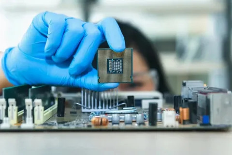
#semiconductor assembly testing
Explore tagged Tumblr posts
Visit Tumblr Blog
Explore Tumblr blogs with no restrictions, modern design and the best experience.
Last Seen Tumblr Blogs


Fun Fact
Tumblr’s website traffic is steadily declining.
Text
Semiconductor Assembly and Testing Services (SATS) Market Growth Driven by AI, IoT, and 5G Technologies
The Semiconductor Assembly and Testing Services (SATS) market is witnessing remarkable growth, driven by the increasing demand for advanced semiconductor packaging and testing solutions. As industries such as artificial intelligence, 5G connectivity, automotive electronics, and the Internet of Things (IoT) expand, the need for efficient and high-performance chips is surging. This has led to the rapid adoption of outsourcing models, where semiconductor manufacturers rely on SATS providers for cost-effective and technologically advanced solutions.
Rising Demand for Advanced Semiconductor Packaging
With the growing complexity of semiconductor designs, traditional packaging methods are no longer sufficient to meet modern performance requirements. Advanced packaging technologies such as fan-out wafer-level packaging (FOWLP), system-in-package (SiP), and 2.5D/3D packaging are gaining traction. These innovations enhance chip functionality while reducing size and power consumption, making them essential for next-generation applications like AI processors and autonomous vehicles. SATS providers are investing heavily in these technologies to remain competitive in the evolving market.
Impact of 5G and IoT on Market Expansion
The global rollout of 5G networks and the proliferation of IoT devices are significant drivers of the SATS market. 5G technology demands high-frequency semiconductor components that require precise assembly and testing. Similarly, IoT applications, from smart homes to industrial automation, rely on efficient and reliable semiconductor solutions. SATS companies are focusing on developing new testing methodologies to ensure these devices meet stringent performance and reliability standards.
Automotive Electronics and the Need for Rigorous Testing
As automotive technology advances, semiconductor components play a crucial role in electric vehicles (EVs), autonomous driving systems, and advanced driver-assistance systems (ADAS). These applications require highly reliable and durable chips that can withstand harsh environmental conditions. SATS providers are enhancing their testing capabilities to address the automotive industry's stringent safety and performance standards. The growing adoption of electric and autonomous vehicles is expected to drive further demand for specialized semiconductor testing services.
Outsourcing Trends and Cost-Effective Solutions
Many semiconductor companies are increasingly outsourcing their assembly and testing processes to SATS providers to optimize costs and streamline production. This trend is particularly prevalent among fabless semiconductor firms that focus on chip design while relying on external partners for manufacturing and testing. Outsourcing enables semiconductor companies to scale operations quickly, access advanced technologies, and reduce capital expenditures, making it a preferred strategy in the industry.
Challenges and Opportunities in the SATS Market
Despite the promising growth of the SATS market, challenges such as supply chain disruptions, rising production costs, and geopolitical uncertainties impact market stability. However, these challenges also create opportunities for innovation and strategic partnerships. Companies that invest in automation, artificial intelligence-driven testing, and sustainable manufacturing practices are likely to gain a competitive edge. Additionally, the shift towards localized semiconductor production in regions like the U.S. and Europe is expected to reshape the global SATS landscape.
Conclusion
The Semiconductor Assembly and Testing Services (SATS) market is at the forefront of technological advancements, driven by increasing demand for high-performance and energy-efficient chips. With continuous innovation in packaging, testing, and automation, SATS providers are playing a crucial role in shaping the semiconductor industry's future. As emerging applications like AI, 5G, and electric vehicles continue to expand, the market is poised for sustained growth, offering significant opportunities for both established players and new entrants.
1 note
·
View note
Text
https://introspectivemarketresearch.com/reports/outsourced-semiconductor-assembly-and-test-services-market/
#Outsourced Semiconductor Assembly and Test Services Market Size#Outsourced Semiconductor Assembly and Test Services Market Share#Outsourced Semiconductor Assembly and Test Services Market Growth#Outsourced Semiconductor Assembly and Test Services Market Trends#Outsourced Semiconductor Assembly and Test Services Market Forecast Analysis#Outsourced Semiconductor Assembly and Test Services Market Segmentation#Outsourced Semiconductor Assembly and Test Services Market 2024#Outsourced Semiconductor Assembly and Test Services Market CAGR#Outsourced Semiconductor Assembly and Test Services Market Analyzer Industry
0 notes
Text
Outsource Semiconductor Assembly and Testing Services (OSAT Services) Market Trends, Growth, Top Companies, Revenue, and Forecast to 2032
Outsource Semiconductor Assembly and Testing Services (OSAT services) have become essential for semiconductor manufacturers aiming to streamline operations and enhance productivity. These services encompass a range of critical functions, including the assembly, packaging, and testing of semiconductor devices, allowing manufacturers to focus on core activities such as design and fabrication. By leveraging the expertise and specialized equipment of OSAT providers, companies can optimize their processes, improve product quality, and reduce time-to-market.
The OSAT sector is experiencing robust growth, driven by increasing demands for sophisticated semiconductor solutions across various industries. As technology advances, devices are becoming more complex, necessitating specialized assembly and testing capabilities. OSAT providers are continuously innovating, offering advanced packaging solutions that meet the performance and reliability requirements of next-generation applications, from consumer electronics to automotive and industrial sectors.
The Outsource Semiconductor Assembly and Testing Services (OSAT services) Market is expanding as semiconductor manufacturers increasingly outsource assembly and testing processes to enhance efficiency, reduce costs, and focus on core competencies amid rising demand for semiconductor products.
Future Scope
The future of OSAT services is promising, with substantial growth anticipated as semiconductor technology continues to evolve. As the industry shifts towards miniaturization and integration, there will be a growing need for advanced packaging solutions that can accommodate high-density designs and complex functionalities. OSAT providers are positioned to play a crucial role in meeting these needs, offering expertise in innovative packaging techniques such as system-in-package (SiP) and 3D packaging.
Moreover, the increasing emphasis on sustainability will influence OSAT services, prompting providers to adopt eco-friendly materials and processes. As manufacturers seek to reduce their environmental impact, OSAT providers will need to innovate in ways that minimize waste and promote recycling within assembly and testing operations. This shift towards sustainability will be essential for compliance with evolving regulations and for meeting consumer expectations for environmentally responsible products.
Trends
Several key trends are shaping the OSAT services market. One significant trend is the increasing adoption of automation in assembly and testing processes. OSAT providers are leveraging advanced robotics and automated systems to enhance efficiency, reduce labor costs, and improve the accuracy of operations. This trend is particularly relevant as manufacturers seek to scale production while maintaining high quality.
Another trend is the growing collaboration between semiconductor manufacturers and OSAT providers. As the semiconductor landscape becomes more competitive, partnerships are forming to leverage complementary strengths in design, assembly, and testing. This collaboration is vital for accelerating product development cycles and ensuring that new technologies are brought to market efficiently.
Application
OSAT services find applications across various sectors, including consumer electronics, automotive, telecommunications, and industrial automation. In consumer electronics, OSAT providers play a critical role in ensuring that devices such as smartphones, tablets, and wearables are assembled and tested to meet rigorous quality standards. This attention to quality is essential for delivering reliable products in a fast-paced market.
In the automotive sector, OSAT services are indispensable for the assembly and testing of semiconductor components used in advanced driver-assistance systems (ADAS), power management, and infotainment systems. The reliability of these components is paramount, as they directly impact vehicle safety and performance.
Telecommunications also relies heavily on OSAT services, with providers ensuring that semiconductor components used in network infrastructure meet stringent performance and reliability standards. As the industry transitions to 5G and beyond, OSAT providers will be instrumental in supporting the development of next-generation communication technologies.
Key Points
Essential for streamlining semiconductor manufacturing operations.
Driven by the increasing complexity of semiconductor devices across industries.
Promising future with growth opportunities in advanced packaging and sustainability.
Trends include automation and collaboration between manufacturers and OSAT providers.
Applied in consumer electronics, automotive, telecommunications, and industrial sectors.
Read More Details: https://www.snsinsider.com/reports/outsourced-semiconductor-assembly-and-test-services-market-4535
Contact Us:
Akash Anand — Head of Business Development & Strategy
Email: [email protected]
Phone: +1–415–230–0044 (US) | +91–7798602273 (IND)
0 notes
Text
#Infineon Technologies#MemorandumofUnderstanding#supplychains#Semiconductor Assembly and Test#electronicsnews#technologynews
0 notes
Text
Vibrant Gujarat: Tata Group's Bold Move with Semiconductor Plant in Dholera
In a significant stride towards technological advancement and industrial growth. Tata Group, under the leadership of Chairman N Chandrasekaran, has unveiled plans to establish. A state-of-the-art semiconductor fabrication plant in Dholera, Gujarat. This ambitious project, slated to commence operations in 2024. Was officially announced during the 10th Vibrant Gujarat Global Summit, marking. A…

View On WordPress
#tata electronics#Tata group plans for a semiconductor factory in Dholera#Tata group plans for a semiconductor factory in Gujarat#Tata group plans for a semiconductor factory in India#Tata group plans for a semiconductor in india#tata semiconductor assembly and test private limited#tata semiconductor investment#tata semiconductor manufacturing company name#tata semiconductor manufacturing company share price#tata semiconductor manufacturing plant in india#tata semiconductor plant location
0 notes
Text
OSAT companies in mainland China lower chip packaging prices
August 25, 2023 /SemiMedia/ — According to industry insiders, OSAT (Outsourced Semiconductor Assembly and Testing) companies in mainland China are lowering prices to win more orders. The utilization rate of mature wire-bonding and mid-to-high-end flip-chip packaging processes in chip packaging has not yet changed significantly, but OSAT companies in mainland China can provide more substantial…
View On WordPress
#electronic components news#Electronic components supplier#Electronic parts supplier#Semiconductor assembly and testing
0 notes
Text
Launch of STS-80 Columbia


"The Space Shuttle Columbia lifts off from the Kennedy Space Center's (KSC) Launch Pad 39B at 2:55:47 p.m. (EST), November 19, 1996. Onboard are astronauts Kenneth D. Cockrell, mission commander; Kent V. Rominger, pilot; along with Story Musgrave, Tamara E. Jernigan and Thomas D. Jones, all mission specialists. The two primary payloads for STS-80 stowed in Columbia's cargo bay for later deployment and testing are the Wake Shield Facility (WSF-3) and the Orbiting and Retrievable Far and Extreme Ultraviolet Spectrometer (ORFEUS) with its associated Shuttle Pallet Satellite (SPAS)."

Columbia inflight

"This mission patch for mission STS-80 depicts the Space Shuttle Columbia and the two research satellites its crew deployed into the blue field of space. The uppermost satellite is the Orbiting Retrievable Far and Extreme Ultraviolet Spectrograph-Shuttle Pallet Satellite (ORFEUS-SPAS), a telescope aimed at unraveling the life cycles of stars and understanding the gases that drift between them. The lower satellite is the Wake Shield Facility (WSF), flying for the third time. It will use the vacuum of space to create advanced semiconductors for the nation's electronics industry. ORFEUS and WSF are joined by the symbol of the Astronaut Corps, representing the human contribution to scientific progress in space. The two bright blue stars represent the mission's Extravehicular Activities (EVA), final rehearsals for techniques and tools to be used in assembly of the International Space Station (ISS). Surrounding Columbia is a constellation of 16 stars, one for each day of the mission, representing the stellar talents of the ground and flight teams that share the goal of expanding knowledge through a permanent human presence in space."
Date: November 19, 1996
NASA ID: KSC-96PC-1290, KSC-96PC-1292, KSC-96PC-1285, KSC-96PC-1284, KSC-96PC-1292, KSC-96PC-1293, STS080-S-003, KSC-96PC-1288, KSC-96PC-1286, KSC-96PC-1287, MSFC-9611692
#STS-80#Space Shuttle#Space Shuttle Columbia#Columbia#OV-102#Orbiter#NASA#Space Shuttle Program#Launch#LC-39B#Kennedy Space Center#KSC#Florida#November#1996#my post
106 notes
·
View notes
Text

Nature-inspired solar lasers could sustainably power space missions
International scientists, including a team from Heriot-Watt University, has announced plans to develop a revolutionary new way of harvesting solar energy in space.
The new technology would directly convert sunlight into laser beams, facilitating the transmission of power over vast distances, such as between satellites, from satellites to lunar bases, or even back to Earth. The approach is inspired by the way bacteria and other plants and organisms convert light energy into chemical energy—a process known as photosynthesis. Repurposing natural photosynthetic structures from nature will form a key component in the new laser technology.
If successful, their innovative technology could help global space agencies to power future endeavors such as lunar bases or missions to Mars, as well as open new pathways for terrestrial wireless power transmission and sustainable energy solutions globally.
The APACE project brings together researchers from the U.K., Italy, Germany and Poland to create the new type of solar-powered lasers, which will provide reliable, efficient power for the growing number of satellites and future space missions.
The system will repurpose light harvesting antennas of certain photosynthetic bacteria, which are highly efficient at absorbing ambient solar light and channeling its energy to a desired target location as part of their photosynthetic cycle.
The team plans to realize their idea under laboratory conditions first, before testing and refining its suitability for deployment into the space environment.
The researchers will begin by extracting and studying the natural light-harvesting machinery from specific types of bacteria that have evolved to survive in extremely low light conditions. These bacteria have specialized molecular antenna structures that can capture and channel almost every photon of light they receive—making them nature's most efficient solar collectors.
In parallel, the team will develop artificial versions of these structures and new laser materials that can work with both natural and artificial light-harvesters. These components will then be combined into a new type of laser material and tested in increasingly larger systems.
Unlike conventional semiconductor solar panels, which convert sunlight into electricity, their bio-inspired system builds on a sustainable organic platform with the potential for replication in space. It would then allow for the direct distribution of power without relying on an electric intermediary.
Professor Erik Gauger from the Institute of Photonics and Quantum Sciences at Heriot-Watt University is leading the theoretical modeling aspects of the project.
He explains, "Sustainable generation of power in space, without relying on perishable components sent from Earth represents a big challenge. Yet, living organisms are experts at being self-sufficient and harnessing self-assembly. Our project not only takes biological inspiration but goes one step beyond by piggybacking on functionality that already exists in the photosynthetic machinery of bacteria to achieve a breakthrough in space power.
"Our APACE project aims to create a new type of laser powered by sunlight. Regular sunlight is usually too weak to power a laser directly, but these special bacteria are incredibly efficient at collecting and channeling sunlight through their intricately designed light harvesting structures, which can effectively amplify the energy flux from sunlight to the reaction center by several orders of magnitude. Our project will make use of this level of amplification to convert sunlight into a laser beam without relying on electrical components.
"We already know it is possible to grow bacteria in space, for example through studies on the International Space Station. Some tough bacteria have even survived exposure to open space! If our new technology can be built and used on space stations, it could help to generate power locally and even offer a route to sending power to satellites or back to Earth using infrared laser beams.
"This technology has the potential to revolutionize how we power space operations, making exploration more sustainable while also advancing clean energy technology here on Earth. All major space agencies have lunar or Mars missions in their plans and we hope to help power them."
The research team expects to have its first prototype ready for testing within three years.
7 notes
·
View notes
Text
Ratan Tata's Business Strategy

In a strategic move, the Ratan Tata-led Tata Group has partnered with Nasdaq-listed American chip maker Analog Devices (ADI) to explore semiconductor manufacturing opportunities in India. This collaboration, announced last week, marks a significant milestone in India’s push towards self-reliance in semiconductor production.
Tata and ADI’s Major Partnership
Tata Electronics, Tata Motors, and Tejas Networks signed a Memorandum of Understanding (MoU) with Analog Devices to enhance their strategic and business cooperation. The goal of the partnership is to explore the potential for semiconductor manufacturing within India. ADI’s semiconductor products are expected to be utilized across Tata Group’s key applications, including electric vehicles (EVs) and network infrastructure.
This collaboration aligns with India’s ambitions to strengthen its semiconductor industry and make a significant contribution to the global supply chain. The Tata Group had already received approval from the Indian government to establish semiconductor assembly, testing, and fabrication facilities within the nation.
Tata’s $14 billion semiconductor investment
Tata Group, a 156-year-old conglomerate with a diverse business portfolio, has committed a massive $14 billion to establish India’s first semiconductor fabrication plant in Gujarat along with a chip assembly and testing plant in Assam. This investment reflects Tata’s dedication to building a strong domestic semiconductor ecosystem.
The construction of these plants, approved by the government earlier this year, is a key step in reducing India’s dependence on semiconductor imports while positioning the country as a significant player in the global tech industry.Read More-https://voiceofentrepreneur.life/
2 notes
·
View notes
Text
US launches $1.6B bid to outpace Asia in packaging tech
New Post has been published on https://thedigitalinsider.com/us-launches-1-6b-bid-to-outpace-asia-in-packaging-tech/
US launches $1.6B bid to outpace Asia in packaging tech
.pp-multiple-authors-boxes-wrapper display:none; img width:100%;
The US is betting big on the future of semiconductor technology, launching a $1.6 billion competition to revolutionise chip packaging and challenge Asia’s longstanding dominance in the field. On July 9, 2024, the US Department of Commerce unveiled its ambitious plan to turbocharge domestic advanced packaging capabilities, a critical yet often overlooked aspect of semiconductor manufacturing.
This move, part of the Biden-Harris Administration’s CHIPS for America program, comes as the US seeks to revitalise its semiconductor industry and reduce dependence on foreign suppliers. Advanced packaging, a crucial step in semiconductor production, has long been dominated by Asian countries like Taiwan and South Korea. By investing heavily in this area, the US aims to reshape the global semiconductor landscape and position itself at the forefront of next-generation chip technology, marking a significant shift in the industry’s balance of power.
US Secretary of Commerce Gina Raimondo emphasised the importance of this move, stating, “President Biden was clear that we need to build a vibrant domestic semiconductor ecosystem here in the US, and advanced packaging is a huge part of that. Thanks to the Biden-Harris Administration’s commitment to investing in America, the US will have multiple advanced packaging options across the country and push the envelope in new packaging technologies.”
The competition will focus on five key R&D areas: equipment and process integration, power delivery and thermal management, connector technology, chiplets ecosystem, and co-design/electronic design automation. The Department of Commerce anticipates making several awards of approximately $150 million each in federal funding per research area, leveraging additional investments from industry and academia.
This strategic investment comes at a crucial time, as emerging AI applications are pushing the boundaries of current technologies. Advanced packaging allows for improvements in system performance, reduced physical footprint, lower power consumption, and decreased costs – all critical factors in maintaining technological leadership.
The Biden-Harris Administration’s push to revitalise American semiconductor manufacturing comes as the global chip shortage has highlighted the risks of overreliance on foreign suppliers. Asia, particularly Taiwan, currently dominates the advanced packaging market. According to a 2021 report by the Semiconductor Industry Association, the US accounts for only 3% of global packaging, testing, and assembly capacity, while Taiwan holds a 54% share, followed by China at 16%.
Under Secretary of Commerce for Standards and Technology and National Institute of Standards and Technology (NIST) Director Laurie E. Locascio outlined an ambitious vision for the program: “Within a decade, through R&D funded by CHIPS for America, we will create a domestic packaging industry where advanced node chips manufactured in the US and abroad can be packaged within the States and where innovative designs and architectures are enabled through leading-edge packaging capabilities.”
The announcement builds on previous efforts by the CHIPS for America program. In February 2024, the program released its first funding opportunity for the National Advanced Packaging Manufacturing Program (NAPMP), focusing on advanced packaging substrates and substrate materials. That initiative garnered significant interest, with over 100 concept papers submitted from 28 states. On May 22, 2024, eight teams were selected to submit complete applications for funding of up to $100 million each over five years.
According to Laurie, the goal is to create multiple high-volume packaging facilities by the decade’s end and reduce reliance on Asian supply lines that pose a security risk that the US “just can’t accept.” In short, the government is prioritising ensuring America’s leadership in all elements of semiconductor manufacturing, “of which advanced packaging is one of the most exciting and critical areas,” White House spokeswoman Robyn Patterson said.
The latest competition is expected to attract significant interest from the US semiconductor ecosystem and shift that balance. It promises substantial federal funding and the opportunity to shape the future of American chip manufacturing. As the global demand for advanced semiconductors continues to grow, driven by AI, 5G, and other emerging technologies, the stakes for technological leadership have never been higher.
As the US embarks on this ambitious endeavour, the world will see if this $1.6 billion bet can challenge Asia’s stronghold on advanced chip packaging and restore America’s position at the forefront of semiconductor innovation.
(Photo by Braden Collum)
See also: Global semiconductor shortage: How the US plans to close the talent gap
Want to learn more about AI and big data from industry leaders? Check out AI & Big Data Expo taking place in Amsterdam, California, and London. The comprehensive event is co-located with other leading events including Intelligent Automation Conference, BlockX, Digital Transformation Week, and Cyber Security & Cloud Expo.
Explore other upcoming enterprise technology events and webinars powered by TechForge here.
Tags: ai, AI semiconductor, artificial intelligence, chips act, law, legal, Legislation, Politics, semiconductor, usa
#2024#5G#Accounts#Administration#ai#ai & big data expo#AI semiconductor#America#amp#applications#Art#artificial#Artificial Intelligence#Asia#automation#betting#biden#Big Data#billion#Business#challenge#China#chip#chip shortage#chips#chips act#Cloud#Commerce#competition#comprehensive
3 notes
·
View notes
Text
Semiconductor Capital Equipment Market Size Booms with Rising Demand for Advanced Chip Manufacturing
The Semiconductor Capital Equipment Market is witnessing significant expansion, driven by the global surge in demand for semiconductors across industries such as consumer electronics, automotive, healthcare, telecommunications, and industrial automation. As chip complexity and miniaturization evolve, manufacturers increasingly rely on advanced capital equipment to enhance precision, scale, and cost-efficiency in production.
This sector includes the essential tools, machines, and infrastructure used in every phase of semiconductor fabrication—lithography, deposition, etching, testing, and packaging. The industry's strategic importance has only grown with the rise of artificial intelligence (AI), 5G, electric vehicles (EVs), and edge computing.
Key Growth Drivers of the Semiconductor Capital Equipment Market
1. Soaring Chip Demand Across Verticals From smartphones and laptops to automotive sensors and medical imaging devices, semiconductors are now deeply embedded in modern life. As a result, foundries and integrated device manufacturers (IDMs) are expanding their fabrication capabilities—pushing capital equipment investments to new highs.
2. Rise of Advanced Nodes and 3D Structures With the transition to sub-5nm nodes and technologies like FinFETs and Gate-All-Around (GAA), manufacturers need next-generation tools capable of ultra-precise etching, inspection, and photolithography. EUV (Extreme Ultraviolet) lithography, in particular, is reshaping capital equipment demands.
3. Government Support and National Chip Strategies The semiconductor supply chain has become a national security priority. Governments across the U.S., Europe, South Korea, Taiwan, and China are offering subsidies and grants to boost domestic chip production—fueling equipment procurement and R&D investment.
4. Shift Toward Smart Manufacturing (Industry 4.0) Automation, AI-driven predictive maintenance, and real-time monitoring are redefining how fabs operate. Capital equipment now integrates advanced software, robotics, and sensor systems—enabling higher yield, lower downtime, and better cost control.
Market Segmentation Snapshot
The Semiconductor Capital Equipment Market can be categorized by:
Equipment Type: Front-end (lithography, etching, doping), Back-end (assembly, packaging, testing)
Application: Foundry, IDM, OSAT (Outsourced Semiconductor Assembly and Testing)
End Use: Consumer Electronics, Automotive, Healthcare, Industrial, IT & Telecommunication
The front-end equipment segment dominates due to the high cost and technological intensity of lithography and wafer fabrication tools.
Leading Market Players
Top companies shaping the landscape include:
ASML
Applied Materials
Lam Research
Tokyo Electron Limited
KLA Corporation
Teradyne
Advantest
These companies are not only innovating hardware but also enhancing software capabilities for defect detection, process control, and yield optimization.
Challenges in the Market
Despite high demand, the market faces a few hurdles:
Global chip supply chain disruptions
High capital expenditure and long ROI periods
Skilled labor shortages in advanced tool operation
Geopolitical tensions impacting export regulations
However, the long-term outlook remains strong, with strategic partnerships and regional diversification emerging as solutions to mitigate these risks.
Regional Insights
Asia-Pacific holds the largest share, with Taiwan, South Korea, Japan, and China leading in both manufacturing and consumption.
North America is a hub for R&D and fab expansion—especially in the U.S., driven by the CHIPS and Science Act.
Europe is investing heavily in semiconductor sovereignty through initiatives like the EU Chips Act.
Future Outlook: Building the Backbone of Tomorrow’s Tech
The semiconductor capital equipment industry is not just a subset of tech—it’s the enabler of all future innovations. From powering AI algorithms to enabling quantum computing and 6G networks, these machines form the backbone of digital transformation.
With continuous advancements in EUV lithography, metrology tools, and wafer inspection, this market will remain one of the most strategically vital and innovation-intensive sectors globally.
Trending Report Highlights
Explore cutting-edge tech markets driving the future of digital infrastructure:
Power Amplifier Market
Speech Recognition Market
Intelligent Railway Transport System (IRTS) Market
Intelligent Airways Transportation System (IATS) Market
Robotic Process Automation (RPA) Market
Touch Screen Controllers Market
Industry 4.0 Market
Hardware Security Modules (HSM) Market
Personal Service Robotics Market
3D XPoint Technology Market
Conclusion
The Semiconductor Capital Equipment Market is at the heart of the global technology race. As demand for smarter, faster, and smaller electronics grows, capital equipment will remain the silent powerhouse behind every chip that shapes our connected world.
0 notes
Text
#Outsourced Semiconductor Assembly and Test Services Market Size#Outsourced Semiconductor Assembly and Test Services Market Share#Outsourced Semiconductor Assembly and Test Services Market Growth#Outsourced Semiconductor Assembly and Test Services Market Trends#Outsourced Semiconductor Assembly and Test Services Market Forecast Analysis#Outsourced Semiconductor Assembly and Test Services Market Segmentation#Outsourced Semiconductor Assembly and Test Services Market 2024#Outsourced Semiconductor Assembly and Test Services Market CAGR#Outsourced Semiconductor Assembly and Test Services Market Analyzer Industry
0 notes
Text
Top Semiconductor Stocks in India to Watch in 2025 – Finowings
Explore the top semiconductor stocks in India for 2025 with Finowings. Discover key companies driving India's chip industry growth and investment potential in the semiconductor sector.

Semiconductor Stocks in India: Key Picks for 2025
India's push toward becoming a global semiconductor hub has opened exciting investment opportunities. With strong government support through initiatives like the PLI scheme and the India Semiconductor Mission, domestic companies are stepping up their presence in chip design, packaging, and electronic manufacturing. While India is still building its semiconductor manufacturing base, several listed companies are already contributing significantly to the ecosystem. For investors looking to benefit from this trend, keeping an eye on semiconductor stocks in India can be a smart move.
One of the top names in this space is Tata Elxsi, which is deeply involved in chip design and embedded systems. The company serves clients across the automotive, healthcare, and electronics industries, and its consistent financial performance makes it a preferred choice for long-term investors.
Another key player is Dixon Technologies, known for its stronghold in electronics manufacturing services. With growing interest in semiconductor assembly and packaging, Dixon’s expansion into this space is backed by government incentives and a clear growth roadmap.
MosChip Technologies is a lesser-known name but holds potential. It works on custom chip design (ASICs) and mixed-signal IPs, which are essential in IoT, consumer electronics, and industrial automation. As the market for smart devices grows, MosChip stands to benefit from increased demand.
Among the pure semiconductor-focused companies, SPEL Semiconductor deserves mention. It is India’s only listed firm offering outsourced semiconductor assembly and testing (OSAT). Though smaller in scale, it occupies a niche with limited competition, and its relevance is expected to grow as India builds more fabless and fab-support infrastructure.
Also worth watching is RIR Power Electronics, which deals in power semiconductor components such as rectifiers and modules. These are crucial in renewable energy, electric vehicles, and industrial automation sectors that are expanding rapidly and will require localized semiconductor solutions.
Why Consider Semiconductor Stocks in India?
India’s electronics demand is skyrocketing—from mobile phones and electric vehicles to defense equipment and AI-enabled devices. The country aims to reduce dependence on imports and promote domestic manufacturing. This shift is already reflected in investor interest and company earnings.
While large-scale chip fabrication units are still under development, companies involved in design, testing, and packaging are gaining momentum. They require lower capital, scale faster, and often serve international clients, giving them an edge.
Final Thoughts from Finowings
If you're an investor looking for exposure to one of the most promising sectors of the future, semiconductor stocks in India offer a strategic entry point. Companies like Tata Elxsi, Dixon Technologies, MosChip, SPEL, and RIR Power are shaping India's semiconductor journey in their own ways. With strong policy support and rising demand, this sector is expected to generate strong returns over the coming years. However, it's wise to evaluate the business model, scalability, and financials of each stock before investing.
0 notes
Text
3D Machine Vision Market Size, Share, Trends, Forecast & Growth Analysis 2034

3D Machine Vision Market is on a promising growth trajectory, expected to rise from $2.2 billion in 2024 to $4.0 billion by 2034, expanding at a CAGR of 5.8%. This market revolves around cutting-edge systems that enable machines to “see” and interpret the world in three dimensions, a technological leap that is transforming industrial operations. From high-precision inspections in automotive manufacturing to quality control in food packaging, 3D machine vision systems are helping businesses enhance accuracy, reduce defects, and automate complex tasks.
By merging high-resolution cameras, smart sensors, and intelligent software, 3D machine vision brings the power of depth perception and object recognition into industrial environments. As factories adopt Industry 4.0 and smart automation principles, the relevance of 3D vision systems is only expected to increase.
Click to Request a Sample of this Report for Additional Market Insights: https://www.globalinsightservices.com/request-sample/?id=GIS33034
Market Dynamics
The market’s momentum is largely driven by the rising need for industrial automation, quality assurance, and defect detection. The hardware segment dominates with cameras, sensors, and lighting systems, essential for capturing clear and precise images. Meanwhile, the software component — particularly AI-powered analytics — is gaining ground rapidly, enabling real-time decision-making and predictive maintenance.
Several industries are adopting these systems for different functions: automotive for inspection and assembly, electronics for circuit testing, logistics for vision-guided robotics, and healthcare for precise diagnostics and device manufacturing. However, the market does face challenges like high initial setup costs, integration complexity, and a shortage of skilled professionals, especially for small and medium enterprises.
Key Players Analysis
The competitive landscape of the 3D machine vision market features some of the world’s leading automation and imaging companies. Cognex Corporation, Basler AG, and Keyence Corporation are at the forefront, continuously innovating to improve resolution, processing speed, and system compatibility. These giants invest heavily in R&D to stay ahead in a market where performance and precision are key.
Alongside them, emerging players such as Opto Engineering, Matrix Vision, and Micro-Epsilon are making significant strides by offering specialized and scalable solutions tailored to evolving customer needs. These companies are carving out their niches by focusing on affordability, customization, and integration capabilities.
Regional Analysis
Asia Pacific leads the global 3D machine vision market, fueled by massive industrialization and technological investments in China, Japan, and South Korea. These nations are investing in smart manufacturing initiatives that rely heavily on 3D vision technologies. Government-backed programs in these countries support automation in industries like automotive and semiconductors, further strengthening the region’s dominance.
North America, especially the United States, is another stronghold, owing to its advanced industrial base and robust investment in emerging technologies. Companies here are early adopters of AI-integrated 3D vision, with major applications in logistics and medical equipment manufacturing.
Europe, led by Germany and the UK, is also making significant progress. The region’s strong focus on Industry 4.0, sustainability, and product precision has made 3D vision systems a staple in high-tech factories. The automotive and electronics sectors, in particular, are key users driving innovation and adoption across the continent.
Recent News & Developments
The past few months have seen several notable moves in the industry. Cognex Corporation partnered with a leading robotics firm to integrate 3D vision into fully automated manufacturing cells, boosting productivity and inspection accuracy. Keyence Corporation unveiled a next-generation 3D vision system capable of detecting micro-defects in ultra-high-speed environments.
Additionally, a prominent European firm was acquired by a global automation leader in a move to expand their vision tech portfolio. In the U.S., new regulations aim to standardize safety protocols for industrial machine vision, which could influence adoption across sectors. Investment in startups focused on AI-driven 3D vision solutions is also ramping up, indicating a strong future pipeline of innovations.
Browse Full Report : https://www.globalinsightservices.com/reports/3d-machine-vision-market/
Scope of the Report
Looking forward, the 3D machine vision market is poised for expansive growth. As businesses increasingly lean into automation, the demand for intelligent, adaptive, and highly accurate vision systems will continue to climb. Key opportunities lie in the expansion of vision-guided robotics, automated quality control, and smart logistics.
With AI and machine learning becoming core components of industrial technologies, vision systems are evolving from basic imaging tools to decision-making enablers. Companies that invest in smart, scalable, and sustainable solutions will be best positioned to lead in this rapidly evolving landscape.
#3dmachinevision #industrialautomation #smartmanufacturing #aiintegration #visiontechnology #qualityinspection #automatedsystems #roboticvision #industry40 #manufacturinginnovation
Discover Additional Market Insights from Global Insight Services:
Mosquito Repellent Market ; https://linkewire.com/2025/05/23/mosquito-repellent-market-2/
Oilfield Chemicals Market : https://linkewire.com/2025/05/23/oilfield-chemicals-market/
Aseptic Packaging Market : https://linkewire.com/2025/05/23/aseptic-packaging-market/
Ceiling Tiles Market : https://linkewire.com/2025/05/23/ceiling-tiles-market/
Compressor Oil Market ;https://linkewire.com/2025/05/23/compressor-oil-market-2/
About Us:
Global Insight Services (GIS) is a leading multi-industry market research firm headquartered in Delaware, US. We are committed to providing our clients with highest quality data, analysis, and tools to meet all their market research needs. With GIS, you can be assured of the quality of the deliverables, robust & transparent research methodology, and superior service.
Contact Us:
Global Insight Services LLC 16192, Coastal Highway, Lewes DE 19958 E-mail: [email protected] Phone: +1–833–761–1700 Website: https://www.globalinsightservices.com/
0 notes
Text
The Advantages of Fanless Industrial PCs in Clean Room Settings
Clean room environments are critical in industries where airborne contaminants can compromise product quality or safety. Whether in semiconductor fabrication, pharmaceutical manufacturing, biotechnology labs, or aerospace component assembly, the integrity of the environment is paramount. One often overlooked yet essential component in maintaining this integrity is the computing hardware used in these spaces. Traditional PCs with fans introduce risks that can undermine the sterile or particle-controlled nature of clean rooms. Enter fanless industrial PCs—a revolutionary solution tailored for such sensitive applications.
The Nature of Clean Room Requirements
Clean rooms operate under stringent regulations to control particulate matter, humidity, temperature, and other variables. Classification systems like ISO 14644-1 define how many particles are permitted per cubic meter of air. Even a minor fluctuation can lead to contamination that disrupts operations or damages products. Equipment introduced into these environments must therefore be designed to minimize any particle emissions, vibrations, or thermal disruptions. Standard computers, with their mechanical cooling systems, are ill-suited for such settings.
Most conventional PCs rely on fans to dissipate heat generated by internal components. While effective at cooling, these fans can become liabilities in clean rooms. They draw in ambient air, which may contain microscopic contaminants, and then circulate it within and beyond the chassis. Over time, this airflow can stir up settled particles or introduce new contaminants into the sterile environment. Additionally, fan motors generate vibration and noise, both of which can interfere with precision equipment or testing. One way to avoid this issue is by using a Fanless Industrial PC, which eliminates the need for airflow while enhancing system stability and cleanliness.
Why Fanless Design Matters
Fanless industrial PCs address these challenges by utilizing passive cooling systems. These designs often involve heatsinks, conductive chassis materials, and optimized internal layouts to manage thermal loads without requiring airflow. The result is a completely sealed system that does not move air—and, by extension, does not move particles. This inherently reduces the risk of contamination, making fanless PCs ideal for use in clean rooms where every particle counts.
Beyond eliminating airborne contaminants, fanless PCs are typically housed in sealed enclosures that offer additional protections. These enclosures are resistant to dust, moisture, and chemical exposure, which are not uncommon in clean room processes. The lack of vents and moving parts means these systems can be sterilized or wiped down more easily without compromising internal components. This adds a layer of hygiene and reliability that traditional systems simply can't match. Among the most advanced solutions available today is the BEDROCK R8000, which delivers exceptional thermal performance in a fully enclosed, fanless chassis.
Enhanced Reliability and Longevity
One of the most compelling benefits of fanless industrial PCs is their durability. Without fans, there are fewer moving parts that can fail. This translates to longer operational lifespans and reduced maintenance needs—an essential advantage in environments where downtime is costly or logistically difficult. Sealed designs also prevent dust and debris from accumulating on internal components, preserving performance and minimizing thermal degradation over time.
When integrated into clean room workflows, fanless PCs contribute significantly to operational efficiency. Their silent operation ensures that they do not interfere with acoustic-sensitive equipment or create auditory distractions. Their thermal efficiency supports consistent performance even under continuous load. For industries where data acquisition, process control, and environmental monitoring are crucial, these PCs provide a dependable backbone without introducing new variables.
Many modern clean room facilities are now choosing fanless systems specifically designed for such environments. For instance, a high-quality fanless industrial PC offers not just fanless design but also a compact form factor, wide operating temperature range, and industrial-grade components. These features make them suitable for wall or panel mounting, freeing up workspace and further reducing contamination risks. They also support industrial protocols and real-time operating systems essential for precision control. Another excellent option for such requirements is the BEDROCK R8000, which combines ruggedness and computing power in one reliable platform.
Modular Efficiency Using i.MX8 SOM
The integration of modular components like the i.MX8 SOM brings additional versatility. This system-on-module platform allows for custom configurations that meet specific clean room demands, from processing power to connectivity. It also supports advanced graphical interfaces and machine learning applications, which are increasingly prevalent in automated lab environments. Its low power consumption and passive cooling features align perfectly with clean room standards.
Conclusion
Fanless industrial PCs are transforming the way sensitive industries approach computing within clean room environments. Their passive cooling systems, sealed enclosures, and robust performance make them an indispensable part of contamination-sensitive operations. These systems don't just improve environmental safety—they also enhance operational efficiency, reduce maintenance costs, and extend the lifespan of critical infrastructure.
Moreover, the flexibility of integrating components like the i.MX8 SOM allows industries to tailor computing solutions to highly specific clean room applications. Whether it's controlling laboratory automation, facilitating real-time data acquisition, or supporting machine learning models for diagnostics, fanless systems are more than up to the task.
As technologies like the BEDROCK R8000 and i.MX8 SOM continue to evolve, we can expect even more tailored solutions that marry high performance with environmental integrity. The growing demands of clean room industries—from semiconductor fabrication to biotechnology—require nothing less than uncompromised reliability and innovation. For industries where cleanliness isn't just preferred but mandatory, fanless PCs aren't just a smart choice—they're the only choice.
0 notes