#turnkey PCB Assembly
Explore tagged Tumblr posts
Visit Tumblr Blog
Explore Tumblr blogs with no restrictions, modern design and the best experience.
Last Seen Tumblr Blogs


Fun Fact
Users from the US are the majority of Tumblr visitors.
Text
Learn everything you need to know about turnkey PCB assembly. Discover the benefits, process, and how Viasion provides complete PCB solutions for your projects.
0 notes
Text
PCB Manufacturing in Toronto: Expertise, Services, and Local Industry Insights
Discover PCB manufacturing in Toronto, a hub of innovation and quality in electronic manufacturing services. Learn about the specialized capabilities, technological advancements, and diverse offerings of PCB manufacturers Toronto. Explore how local expertise and cutting-edge facilities contribute to producing high-quality printed circuit boards for various industries and applications worldwide. For more details visit our website www.crimpcircuits.com
#pcb manufacturing toronto#printed circuit board design#metal clad pcb#printed circuits#rigid flex pcb#full turnkey pcb services#turnkey pcb services#pcb parts#eagle software#pcb designing#flexible pcb#pcb assembly#printed circuit board manufacturers#pcb manufacturers in canada#circuit board manufacturers in canada#pcb quote#pcb prototype services in canada
2 notes
·
View notes
Text
Full-Turn Key PCB Manufacturing: Superior Quality, Unmatched Speed, and complete Flexibility
Bringing a PCB design to life requires efficiency, precision, and reliability. That’s where full turnkey PCB manufacturing comes in, offering a seamless process from design and component sourcing to quick turn PCB assembly and final production.
At Bay Area Circuits, we specialize in full turnkey PCB solutions that provide superior quality, unmatched speed, and complete flexibility. Whether you're developing a prototype or preparing for high-volume production, our quick turn PCB assembly ensures rapid turnaround without compromising on quality. By handling everything from procurement to manufacturing, we help reduce costs, minimize errors, and accelerate time to market.
In our latest blog—"Full-Turn Key PCB Manufacturing: Superior Quality, Unmatched Speed, and Complete Flexibility"—we explore how full turnkey PCB services streamline production while guaranteeing top-tier performance. If you’re looking for a hassle-free PCB manufacturing experience, this is a must-read! Read the full blog here: https://67d7ed103fe91.site123.me/blog/full-turn-key-pcb-manufacturing-superior-quality-unmatched-speed-and-complete-flexibility
0 notes
Text
https://www.bloglovin.com/@mefrontechnologies/what-is-turnkey-pcb-assembly-its-benefits
What is Turnkey PCB Assembly and its Benefits
Turnkey PCB assembly is a game-changer for businesses looking for efficiency, reliability, and cost savings in their PCB manufacturing process. By outsourcing to an experienced turnkey provider, companies can eliminate supply chain hassles, improve quality control, and speed up production cycles.
0 notes
Text

Heavy Copper PCB Manufacturing
Over 15 years experiences of thick copper PCB
What is Heavy Copper PCB?
Heavy copper PCB is a circuit board with a copper thickness that is ≥ 3oz per sq. ft in its outer and inner layers. What makes a circuit board classified as a heavy copper PCB is its thicker plating. During the production of heavy copper PCB, copper thickness is enhanced through plated holes and sidewalls. For instance, when a PCB has 2 ounces of copper per sq. ft thickness, it is a standard PCB. However, if it has more than 3oz of copper, it is a heavy copper PCB. Heavy copper PCB is considered a reliable wiring option. Heavy copper PCB is different from extreme copper PCB which features within 20 oz to 200 oz per sq. ft.
What does Heavy Copper PCB offer?
Heavy copper PCB has a lot to offer. It has got some unique features that make it an ideal option for high-end applications. Let’s discuss some of the benefits of this PCB; Great thermal distribution: Due to its copper-plated vias, this PCB offers high thermal resistance. Heavy copper PCB are used in applications that demand high speed and high frequency. You can also use this PCB at harsh temperatures. Mechanical strength: Heavy copper PCB feature great mechanical strength. When this PCB is used, it makes the electrical system durable and robust. Good conductor: Heavy copper circuit boards are a good conductor. They are utilized in the production of electronics due to this feature. They help to link various boards together. These boards can transfer current.
How is Heavy Copper PCB Fabricated?
For the fabrication of heavy copper PCB, plating or etching is often used. The main aim is to add copper thickness to sidewalls and plated holes. The methods used in fabricating heavy copper PCB aren’t far-fetched. Heavy copper PCBs need special etching and plating methods to ensure the extra thickness of copper. Using the normal etching techniques for the fabrication of heavy copper PCBs isn’t ideal. Normal etching methods produce over-etched margins and edge lines that are uneven. PCB producers now use advanced etching and plating methods to achieve straight edges.
Heavy copper PCBs are produced via etching and plating methods. The major aim in the production of this PCB is to add copper thickness through sidewalls and plated-through holes. Heavy copper PCBs have several benefits which make them in high demand. Due to their outstanding features and benefits, they can meet your electrical requirements. These circuit boards will always dissipate heat generated due to heavy currents conduction. Electronics using heavy copper boards have been in use for a long time. Heavy copper can carry high currents. These boards will continue to meet the needs of various applications. High power circuit wirings can be developed using Heavy Copper PCBs. Such a wiring mechanism offers more reliable thermal stress handling and offers fine finishing while incorporating multiple channels on a single layer of a compact board.
Printed circuit boards (PCBs) are usually bonded with a layer of copper foil on a glass epoxy substrate. The thickness of the copper foil is usually 18μm, 35μm, 55μm, and 70μm. The most commonly used copper foil thickness is 35μm. Domestic copper foil thickness is generally 35 ~ 50μm, there are thinner than this such as 10μm, 18μm; And thicker than that like 70μm. The thickness of composite copper foil on 1~ 3mm thick substrate is about 35μm. The thickness of the composite copper foil on the substrate less than 1 mm thick is about 18μm, and the thickness of the cladding copper foil on the substrate thicker than 5mm is about 55μm. If the PCB copper foil thickness is 35μm, printed line width is 1mm, then every 10mm long, its resistance value is about 5mΩ, its inductance is about 4nH. When the di/dt of the digital integrated circuit chip on the PCB is 6mA/ns and the working current is 30mA, the noise voltage generated by each part of the circuit is estimated to be 0.15mV and 24mV according to the resistance value and inductance value of each 10mm printed line. Heavy Copper PCB boards can be made simply by combining two main processes: electroplating and etching. Compared to other PCBs, the circuit is made of a thin layer of copper foil. The copper plates are uniformly laminated with FR4 or other epoxy-based substances. The average weight of a Heavy Copper PCB can be 4 oz. (140μm), which is a better ratio than a copper-shared PCB. Let's look at the benefits.
Heavy Copper PCB Manufacturer & Circuit board Assembly – One-stop service Printed Circuit Boards (PCB) are usually coated with thick copper foil on a glass epoxy substrates commonly thickness of copper foil are 18μm, 35μm, 55μm, and 70μm. The most common copper foil is 35μm. The heavy copper PCB boards can simply be manufactured by two main processes plating and etching in the combine. As compared to other PCBs, the circuit is made of a thin layer of the Copper foil sheet. The plates of copper are laminated uniformly with FR4 or other epoxy-based substance. The average weight of the thick copper PCB weight could be 4oz (140μm), and this ratio is better as compared to another type of PCBs who have copper in common. Let’s check out the benefits of it.
Benefits of Heavy copper PCB Fabrication
Here are some of the advantages of heavy copper PCB, let’s follow them:
1. Favorable circumstances of Heavy Copper PCB
2. Plating innovation in overwhelming copper permitted a mix of plating and carving which causes in straight sidewalls and immaterial undercut.
3. The substantial copper plating creates high-current circuits and control circuits that watches the profoundly thick and straightforward whiskers’ structure.
4. This empowers the board fabricator to build the measure of copper thickness in plated gaps and by means of sidewalls.
5. The blend of substantial copper results on a solitary board called PowerLink.
6. The substantial copper in the PCB likewise encourages in associating with the standard circuits.
7. This lessens layer tally, low impedance control conveyance, littler impressions, and potential cost investment funds.
8. For development purposes, it expands the continuance to warm strains.
9. It has expanded the current conveying limit.
10. Overwhelming copper plating brings higher current through the board and moves the warmth to the outside heat sink
Application and advantage of Heavy Copper PCB in Electronic manufacturing
Heavy Copper PCB is a special PCB, its main characteristic is that the copper thickness is greater than or equal to 2oz. Compared with traditional PCB, Heavy Copper PCB has many advantages in electronic manufacturing. For example, they can withstand higher currents, have better heat dissipation capacity, better mechanical strength and better electrical properties. These characteristics make Heavy Copper PCBs widely used in high power equipment, such as electric vehicles, industrial robots, aerospace, mobile phones, microwave, satellite communications, network base station and other fields.
Take electric vehicle electronic control system as an example, electric vehicle electronic control system is one of the core components of the vehicle, has a very important role. In this kind of high-power electronic equipment, the range of current and voltage changes is very large, and the Heavy Copper PCB has better load capacity and heat dissipation capacity, which can ensure the stability and reliability of the electronic control system. Our customers use Heavy Copper PCBs in the production of electric vehicle electronic control systems to ensure the stability and reliability of the system under high power operating conditions.
When you decide to use a Heavy Copper PCB, you need to choose the right PCB manufacturer, Hitech Circuits will be able to offer copper plates in a variety of thicknesses and specifications to suit your needs. At the same time, you should ensure that your design meets the specifications and requirements of Heavy Copper PCB, including the wiring specifications of Heavy Copper PCB, welding pad specifications, etc. Finally, the right manufacturing process is also key, such as the selection of appropriate drilling, sheet laying and other processing steps to ensure quality.
In short, Heavy Copper PCB plays an irreplaceable role in the production and application of PCB industry, with high power, high current and high cooling effect. Heavy Copper PCB manufacturing process and materials have higher requirements than standard PCB. Hitech Circuits has advanced equipment and professional engineers to supply high quality Heavy Copper PCBs to domestic and international customers.
Heavy Copper circuit board technology introduction
(1) Preparation and plating treatment before plating
The main purpose of thickening copper plating is to ensure that there is enough Heavy Copper coating in the hole to ensure that the resistance value is within the range required by the process. As an insert is fixed position and ensure the connection strength; As surface-packaged devices, some holes only act as conduction holes, which conduct electricity on both sides.
Check item
a. Mainly check the metallization quality status of the hole, and ensure that there is no residue, burr, black hole, hole, etc.;
b. Check whether there is dirt or other residue on the surface of the substrate;
c. Check the number, drawing number, process document and process description of the substrate;
d. Make clear the installation and hanging position, installation and hanging requirements and the plating area that the plating tank can withstand;
e. Plating area and process parameters should be clear to ensure the stability and feasibility of plating process parameters;
f. Clean and prepare the conductive parts, and first energize the solution to make it appear active;
g. Determine whether the composition of the tank is qualified and the status of the surface area of the plate; If the cylindrical anode is used, the consumption must be checked;
h. Check the firmness of the contact parts and the fluctuation range of voltage and current.
(2) Quality control of thickened copper plating
a. Accurately calculate the plating area and refer to the effect of actual production process on current, correctly determine the required value of current, master the change of current in electroplating process, and ensure the stability of plating process parameters;
b. Before electroplating, the commissioning plate is used for test plating, so that the bath is in the activated state;
c. Determine the direction of the total current flow, and then determine the order of the hanging plate. In principle, it should be from far to near; Ensure the uniform distribution of current to any surface;
d. To ensure the uniformity of the coating and the consistency of the coating thickness in the hole, in addition to the technical measures of mixing and filtering, the impact current should be used;
e. Constantly monitor the change of current in the electroplating process to ensure the reliability and stability of current values;
f. Test whether the thickness of the copper plating layer in the hole meets the technical requirements.
(3) copper plating process
In the process of thickening copper plating, the process parameters must be monitored regularly, which often causes unnecessary losses due to subjective and objective reasons. To do a good job of thickening copper plating process, we must do the following aspects:
a. Add a certain value according to the area value calculated by the computer and the empirical constant accumulated in the actual production;
b. According to the calculated current value, in order to ensure the integrity of the coating in the hole, a certain value must be added to the original current value, namely, the impact current, and then return to the original value in a short time;
c. When the electroplating of the circuit board reaches 5 minutes, take out the substrate and observe whether the copper layer on the surface and the inner wall of the hole is complete, and the metal luster in all holes is preferable;
d. A certain distance must be kept between the substrate and the substrate;
e. When the thickened copper plating has reached the required plating time, a certain amount of current should be maintained during the removal of the substrate to ensure that no blackening or darkening will occur on the surface of the substrate or in the hole.
Note:
a. Check process documents, read process requirements and get familiar with lamina chart of substrate machining;
b. Check the surface of the substrate for scratches, indentation, copper exposure and other phenomena;
c. According to the mechanical processing floppy disk test processing, the first part of the pre-inspection, meet the technical requirements before all the workpiece processing;
d. Prepare measuring tools and other tools to be used for monitoring substrate geometry;
e. Select the appropriate milling tool (milling cutter) according to the raw material nature of the machining substrate.
Quality control
a. Strictly implement the first-part inspection system to ensure that the product size meets the design requirements;
b. Select milling processing parameters reasonably according to the raw materials of the circuit board;
c. When fixing the position of the circuit board, it should be carefully clamped to avoid damaging the solder layer and solder resistance layer on the surface of the circuit board;
d. To ensure the consistency of the overall dimension of the substrate, the position accuracy must be strictly controlled;
e. When disassembling and assembling, special attention should be paid to the layer of the substrate to pad the paper, so as to avoid damaging the plating layer on the circuit board surface.
The three characteristics of Heavy Copper PCB
1, bearing large current
When the line width is certain, increasing the copper thickness is equivalent to increasing the section area of the circuit, so the thickening of copper foil can make the circuit board carry more current.
2. Reduce thermal strain
Copper foil has a small conductivity (also known as resistivity, 1.72*10-8ΩΩ·m) through high current condition temperature rise is small, so it can reduce heat, thereby reducing thermal strain.
The conductivity is the resistivity. Metal "conductors" are divided into:
Silver → Copper → gold → aluminum → tungsten → nickel → iron.
3, Good heat dissipation
Copper foil has high thermal conductivity (thermal conductivity of 401W/mK), which can play an important role in improving heat dissipation performance, so it has good heat dissipation;
Thermal conductivity refers to the heat transferred through an area of 1m2 within 1H for a 1m thick material with a surface temperature difference of 1°C under stable heat transfer conditions. The unit is W/m·K.
Based on the above characteristics, it can be seen that Heavy Copper PCB is very suitable for high-current products. It has different characteristics and can better achieve circuit functions.
Application of Heavy Copper PCB
Heavy Copper PCBs have a number of benefits over standard PCBs. In addition, they offer excellent features that make them ideal for specific applications. For example, Heavy Copper PCBs are ideal for defense and military applications, medical devices, and many other fields. As a result, the demand for Heavy Copper PCB is increasing.
Here are some applications of Heavy Copper PCBs:
Solar energy converter
Track traction system
Nuclear power industry
Automobile industry
UPS system
Protective relay
Torque control
Safety and signal system
Welding equipment
Power line motor
Military equipment
What can Heavy Copper PCBs provide?
Heavy Copper PCBs have a lot to offer. It has some unique features that make it ideal for high-end applications. Let's discuss some of the benefits of this PCB;
• Great heat distribution: This PCB provides high thermal resistance due to its copper-plated through-hole. Heavy Copper PCBs are used in applications requiring high speed and high frequency. You can also use this PCB in harsh temperatures.
• Mechanical strength: Heavy Copper PCBs have very high mechanical strength. When used, this PCB makes the electrical system durable and rugged.
• Good conductor: Heavy Copper circuit boards are good conductors. Because of this property, they are used in the production of electronic products. They help hold the various plates together. These plates can transmit electricity.
• Onboard radiators: Heavy Copper PCB provide onboard radiators. Using these plates, you can achieve an effective radiator on a Mosaic surface.
• Large dissipation coefficient: Heavy Copper PCBs are ideal for large components with high power consumption. These PCBs prevent the electrical system from overheating. They dissipate heat effectively.
Hitech Circuits is a professional PCB manufacturer with extensive experience in manufacturing Heavy Copper PCBs, as well as your other product requirements. We support sample and mass production, welcome to your inquiry.
0 notes
Text
“Like a master conductor leading an orchestra, Avalon Technologies harmonizes design, engineering, and production to create the symphony of electronics manufacturing.”
#electronic manufacturing services#EMS#electronic assembly#PCB manufacturing#electronics design services#electronic component manufacturing#OEM services#electronics production#custom electronics#PCB assembly#electronic engineering services#EMS provider#electronic product manufacturing#turnkey manufacturing services#electronics supply chain.
0 notes
Text
PCB Manufacturing-PCB Assembly-Hitech Circuits
Hitech Circuits is a lеаding PCB Manufacturing & PCB Assembly company with more than 20 years experience in the electronics manufacturing industry. We focus on PCB Design, PCB Layout, Circuit board fabrication, Turnkey PCB assembly, and electronic parts sourcing services.
With mature supply chain, talented design team, advanced manufacturing techniques and quality control systems, Hitech is able to provide one-stop electronics manufacturing services and solution for our customers to help them stand out in the marketplace.
We offer a full range of Electronic manufacturing services.
-LED PCB
-Heavy Copper PCB
-Multilayer PCB
-HDI PCB
-Flexible PCB
-Rigid-Flex PCB
-High Speed PCB
-High Frequency PCB
-PCB Reverse Engineering
7 notes
·
View notes
Text
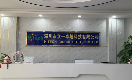
High Volume PCB Assembly by Hitech Circuits Co., Limited in Shenzhen China
Your leading PCB High Volume PCB Assembly supplier in China
With 15 years of experience and high efficiency in PCB assembly and manufacturing, HITECH CIRCUITS is the perfect source for Big Batch PCB assembly on a limited budget. If you are looking for a large PCBA assembly within your budget, we will be your ideal choice. HITECH CIRCUITS has more than 15 years of experience in the OEM/PCBA manufacturing and assembly of printed circuit boards, advanced production technology and equipment, professional engineers and purchasing team to provide our partners with personalized and complete process solutions. HITECH CIRCUITS’s supply chain services deliver supply chain innovation on demand. We offer a bold, yet proven service solution designed to grow market share and profit. Our innovative approach to managing the supply chain offers a complete business model that delivers the talent and transformative tools necessary to create predictability, reliability, and responsiveness across your entire supply chain. Our practitioners are passionate about supply chains. We have spent a generation understanding, refining and building the best in intelligent supply chains. We provide talent on-demand with expertise in data analytics and strategic technologies that can help you predict, plan and respond more effectively.
Some designs require assemblies in small volume, maybe just prototypes, while others require them in high volume. At SMT house, High Volume, Large Volume, or Big Batch PCB Assembly always refers to printed board assembly projects with quantities more than 5K pieces. HitechPCB has the capability to offer high volume PCB assembly services to meet your requirements of high-quality, competitive price, on-time delivery and smooth communication in any manner of full turnkey, consigned and partial turnkey.
Also, if your business is involved in applications that require high-volume PCB assembly, the company to contact is HitechPCB, because we’re a complete turnkey solution for printed circuit boards assembly, we are ideally suited for bulk PCB assembly orders. Our state-of-the-art equipments, large facility and wide range of highly-qualified experts give us the capability of high-volume PCB assembly of up to 9,000,000.
We are also the perfect source if you’re looking for large-order PCB assembly on a budget. Because of our high level of efficiency and more than 10 years of experience with printed circuit board manufacturing and electronics assembly, we offer large printed circuit board orders at surprisingly competitive prices compared to other PCB manufacturers or PCB assembly companies.
Our large order PCB assembly process starts with a tested and practiced set of workflow guidelines for every phase of the process, from pre-order PCB design consultation with professional veteran engineers to PCB fabrication, components sourcing, PCB assembly, PCBA testing, PCBA inspection, PCBA packing and shipping all under the auspices of a highly-skilled production staff. You can be confident that no matter how many circuit boards you order, you will enjoy fast service, low prices and extremely high quality.
With our excellent after-sales service, 24 sales and technical support team, quick response service, we will be your best Big Batch PCB assembly manufacturer inChina. A wide variety of highly qualified experts
Why choose Hitechpcba Big Batch PCB Assembly
Compared to our competitors, Hitechpcba offers large printed circuit board orders at very competitive prices. The risky big batch PCB assembly process begins with a set of tried and tested workflow guidelines. From ordering PCB design to component procurement, manufacturing, testing, assembly, inspection, shipping and packaging. This is all under the guidance of our highly skilled production staff.
No matter how many boards you order, you'll love the fast response service, low cost, and surprisingly high quality.
Whether you are seeking for product designer, electrical engineer, system integrator, manufacturer, or big batch PCB manufacturing and assembly, low cost big batch PCB housing, electronic assembly services, Hitech Circuits PCB Assembly team will be your perfect choice for big batch PCB assembly plant inChina.
Finding Reliable High Volume PCB Assembly Supplier?
When your design passed the prototyping verification after optimization, DFM and DFT check, it’s time to find a manufacturer or a supplier who has ability to perform high volume PCB manufacturing and assembly for you. HITECH CIRCUITS is a one-stop PCB solution provider, no matter which your design stage is located, we always can help in PCB manufacturing, assembly and design. With both design and manufacturing knowledge, we can feedback some suggestions to modify or change your design on the basis of cost-down without sacrificing the quality and performance. What’s more, if choosing our full turnkey PCB assembly service, we will be responsible of BOM sourcing to reduce your workload. Our approach to conducting high volume printed circuit board assembly is founded on a commitment to the highest possible quality, based on IPC standards and our inner quality control processes. In spirit of those high assembly standards, HITECH CIRCUITS developed excellent high-volume assembly capabilities and manufacturing processes relied on our advanced assembly lines in dust-free workshop.
#PCB assembly #Electronic assembly #China PCB manufacturer
1 note
·
View note
Text
Leading PCB Manufacturers in Canada: Quality and Innovation
Discover the top PCB manufacturers in Canada that specialize in providing high-quality printed circuit boards for various industries, including aerospace, automotive, medical, and consumer electronics. These companies offer a range of services, from prototype development to mass production, ensuring precision engineering and compliance with international standards. With state-of-the-art technology and skilled professionals, Canadian PCB manufacturers are committed to delivering innovative solutions, fast turnaround times, and exceptional customer service. Partner with these trusted manufacturers to meet your electronic design and manufacturing needs.
#pcb manufacturing toronto#printed circuit board design#metal clad pcb#printed circuits#rigid flex pcb#full turnkey pcb services#turnkey pcb services#pcb parts#eagle software#pcb designing#flexible pcb#pcb assembly#printed circuit board manufacturers#pcb manufacturers in canada#circuit board manufacturers in canada#pcb quote#pcb prototype services in canada
0 notes
Text

PCB Assembly
Hitech offer turnkey electronics assembly services, including prototype pcb assembly or low & high volume pcb assembly production. Our PCB assembly service always exceed customer’s expectations for quality, price and delivery. We manage the whole process including ordering PCB manufacturing, sourcing components, PCB assembly, and PCBA testing, etc.
What are the Benefits of SMT PCB Assembly?
SMT assembly provides many benefits and some of them are as follows:
It can be used to incorporate small components.
In SMT, the components can be placed on both sides of the board.
It assures high component densities.
Fewer holes need to be drilled for surface mounting than through-hole.
It require low initial costs and time for setting up the mass production.
SMT is the simpler and faster-automated assembly when compared to through-hole.
Errors regarding the component placement can be easily rectified.
Surface mount PCBs feature strong joints, which can easily withstand vibrations.
Circuit Board, PCB assembly & electronics manufacturing service provider from China (hitechcircuits.com)
#pcb design#pcb china#pcb fabrication#pcb board#pcb supplier#pcb manufacturer#pcb factory#aluminum pcb#flex pcb#touhou pcb
1 note
·
View note
Text
Electronics Manufacturing Companies in India: Driving the Future of Tech Production
India is fast becoming a global hub for electronics manufacturing. With increasing demand for digital devices, smart infrastructure, and industrial automation, the country has seen a surge in investments and capacity in this sector. Electronics manufacturing companies in India are now producing high-quality components and complete systems that power everything from smartphones and electric vehicles to medical equipment and defense systems.
Why Electronics Manufacturing Matters Today
In the digital era, electronics are the foundation of nearly every modern device. From the chips in your phone to the control boards in smart homes, electronics manufacturing supports innovation across industries. India’s manufacturing companies are not only meeting domestic demand but are also contributing significantly to global supply chains.
What Electronics Manufacturing Companies in India Offer
The services offered by Indian electronics manufacturers have expanded rapidly in recent years. These include:
PCB design and fabrication
Surface Mount Technology (SMT) assembly
Cable and wire harnessing
Rapid prototyping and NPI (New Product Introduction)
Functional testing and quality assurance
Box build and system-level assembly
Many manufacturers also offer turnkey solutions—from idea to product deployment.
Industries Supported by Electronics Manufacturing
Electronics manufacturing companies in India serve a broad range of sectors, including:
Consumer Electronics – TVs, smartphones, home appliances
Automotive – EV systems, infotainment, ECUs, sensors
Telecommunications – Network equipment, routers, base stations
Industrial Automation – IoT controllers, sensors, embedded systems
Medical Devices – Diagnostic machines, monitoring systems
Aerospace & Defense – Surveillance systems, radar units, navigation components
The ability to adapt to diverse technical needs has made Indian companies global players.
Growth Drivers for Electronics Manufacturing in India
Several factors have accelerated the growth of electronics manufacturing in India:
Government Policies
Initiatives like “Make in India,” PLI (Production Linked Incentive), and EMC 2.0 (Electronics Manufacturing Clusters) have created a fertile ground for domestic and foreign companies to invest in electronics production.
Skilled Workforce
India produces thousands of engineers every year with expertise in electrical, electronics, and embedded systems, supporting high-quality design and production.
Cost-Effective Production
Compared to other countries, India offers competitive production costs without sacrificing quality, making it attractive for long-term manufacturing partnerships.
Manufacturing Hotspots in India
Electronics manufacturing clusters are emerging across the country, each offering specialized capabilities:
Bangalore, Karnataka – Embedded systems and R&D
Noida, Uttar Pradesh – Mobile phone manufacturing
Chennai, Tamil Nadu – EMS and component assembly
Pune, Maharashtra – Automotive electronics and control systems
Hyderabad, Telangana – PCB design, chip testing, and semiconductors
These hubs are supported by industrial parks, logistics infrastructure, and skilled labor.
Advanced Technologies in Use
Modern electronics manufacturing companies in India are leveraging Industry 4.0 practices:
Automated SMT lines
AI-based inspection and testing
Cloud-integrated production systems
IoT-connected assembly equipment
Zero-defect manufacturing goals
These innovations enhance precision, speed, and product reliability while reducing waste and downtime.
Sustainability in Electronics Manufacturing
Environmental responsibility is becoming a key focus area. Many manufacturers are now:
Complying with RoHS and REACH standards
Reducing carbon emissions through green energy adoption
Using recyclable materials in production
Managing e-waste through certified disposal and reuse practices
Sustainable manufacturing isn’t just a trend—it’s an industry standard.
How to Find Electronics Manufacturing Companies in India
Businesses looking for reliable electronics manufacturing partners can turn to platforms like FindingMFG.com. These directories list verified Indian manufacturers with detailed profiles covering services, industries served, certifications, and locations. Using such tools can help you compare, connect, and collaborate with trusted companies that match your project’s requirements.
Conclusion
India’s electronics manufacturing companies are evolving from basic assemblers to full-service tech partners. With the right mix of talent, technology, infrastructure, and policy support, these companies are now capable of delivering complex, high-performance electronics solutions to clients around the world. Whether you're building consumer devices, industrial machines, or aerospace systems, India offers an ideal ecosystem for scalable, reliable, and innovative electronics production.
FAQs
1. What makes electronics manufacturing companies in India globally competitive? India offers a mix of skilled labor, cost-effectiveness, advanced technology adoption, and government support, making its manufacturers globally appealing.
2. What types of products are manufactured by these companies? Products range from PCBs and embedded systems to full electronic assemblies for consumer, automotive, and industrial use.
3. Are electronics manufacturers in India certified to international standards? Yes, many are ISO-certified and comply with global standards such as IPC, RoHS, and REACH.
4. Can small businesses work with electronics manufacturers in India? Absolutely. Many manufacturers offer prototyping, small-batch production, and NPI support for startups and SMEs.
5. How can I contact a reliable electronics manufacturing company in India? B2B platforms like FindingMFG.com help you find and connect with verified, reliable manufacturing companies tailored to your needs.
#electronics manufacturing#electronics manufacturing companies#manufacturing#business#business directory
0 notes
Text
0 notes
Text
The Role of PCB Assembly in Med-Tech and Automotive Sectors

As global industries evolve with smarter, smaller, and more powerful devices, the demand for precision-engineered PCB assembly has skyrocketed — especially in the medical technology (med-tech) and automotive sectors. These industries demand not just high-quality electronics but also speed, reliability, and regulatory compliance. This is where Aimtron Electronics plays a vital role.
Why PCB Assembly Is Critical in Med-Tech
Modern medical devices — from portable ECG machines to imaging systems and wearable diagnostics — rely on compact and high-performance PCBs. In this sector, zero-failure tolerance is a must, as even a minor malfunction can affect patient health and safety.
At Aimtron Electronics, our quick-turn PCB prototyping, BGA assembly expertise, and precision testing services support med-tech innovators in rapidly developing and scaling their products. Our assembly processes are developed in the USA and implemented in India, ensuring global quality standards with local agility.
Automotive Electronics: Reliability Under Pressure
The automotive industry is undergoing a major transformation, driven by electric vehicles (EVs), ADAS (Advanced Driver Assistance Systems), and in-vehicle infotainment. These applications require PCBs that can withstand harsh environments, thermal cycling, and mechanical stress.
Aimtron supports this with:
High-volume SMT and thru-hole PCB assembly
Robust testing procedures to ensure durability and consistency
Electromechanical integration for complete module assembly
Whether it’s battery management systems or advanced lighting controls, Aimtron’s engineering and manufacturing expertise deliver consistent performance for automotive applications.
Global Expertise, Local Execution
With our flagship manufacturing facility in the United States and advanced production lines in Vadodara, Gujarat, Aimtron Electronics offers a seamless global supply chain. Our clients benefit from:
USA-grade quality
Faster development cycles
Cost-effective scalability
Supporting Innovation with Trusted Partnership
Aimtron is more than just a PCB assembly company — we’re your ESDM partner, offering turnkey solutions across product design, manufacturing, and testing. For med-tech and automotive companies looking to bring high-impact electronics to market, Aimtron provides the technical strength, speed, and global reliability you need.
0 notes
Text
“Riding the wave of innovation, Avalon Technologies is not just keeping pace with the electronics manufacturing industry, but setting the rhythm.”
#electronic manufacturing services#EMS#electronic assembly#PCB manufacturing#electronics design services#electronic component manufacturing#OEM services#electronics production#custom electronics#PCB assembly#electronic engineering services#EMS provider#electronic product manufacturing#turnkey manufacturing services#electronics supply chain.
0 notes
Text
The Benefits of Opting for Aimtron PCB Assembly Manufacturing Services in Illinois

In today’s competitive electronics landscape, Original Equipment Manufacturers (OEMs) and product developers are under increasing pressure to reduce time-to-market, enhance product quality, and control costs. Partnering with the right Electronics Manufacturing Services (EMS) provider can make a significant difference—and that’s where Aimtron Corporation, headquartered in Palatine, Illinois, stands out.
Why Choose Aimtron for PCB Assembly in Illinois?
Aimtron Corporation, a trusted name in the electronics manufacturing industry since 2009, delivers state-of-the-art PCB assembly services with a focus on quality, speed, and reliability. Here’s how businesses benefit by choosing Aimtron’s services in Illinois:
1. Expertise in Complex Assemblies
Aimtron brings deep expertise in handling Turnkey PCB Assemblies, including BGA, micro-BGA, Stack BGA, ultra-fine pitch QFP, QFN, and CSP packages. This enables customers to outsource even the most intricate designs with confidence.
2. Quick Turn Prototyping
Time-sensitive projects demand quick action. Aimtron’s quick-turn PCB prototyping services ensure that design iterations are turned around rapidly—without compromising on precision or quality. This allows businesses to accelerate product development cycles.
3. Advanced Testing & Inspection
Every assembly goes through rigorous quality assurance processes including:
Automated Optical Inspection (AOI)
X-Ray Inspection
In-Circuit Testing (ICT)
Functional Testing
Burn-in Testing
Additionally, firmware programming, conformal coating, and potting services are available to meet end-product reliability expectations.
4. Comprehensive Electromechanical & Cable Assembly
From board-level assembly to electromechanical integration and wire harnessing, Aimtron offers end-to-end solutions. This reduces the need for multiple vendors and simplifies the supply chain.
5. Customer-Centric Operations
Aimtron emphasizes customer service, transparency, and responsive communication, making them a reliable partner for both startups and large-scale OEMs across the U.S.
6. USA-Based Manufacturing with Global Standards
Being based in Palatine, Illinois, Aimtron delivers the best of both worlds—domestic responsiveness and global quality benchmarks. This helps companies reduce shipping times, ensure IP protection, and access a knowledgeable U.S.-based engineering team.
7. High-Value Mechanical and Design Engineering Support
More than just an assembly house, Aimtron offers full-stack electronics engineering and design services, including DFM (Design for Manufacturing) and component selection guidance. This ensures your products are optimized from concept to completion.
Conclusions:
Whether you're launching a new product or scaling an existing one, Aimtron Corporation’s PCB assembly and EMS capabilities in Illinois offer the technical strength and operational agility that modern electronics businesses need. With cutting-edge facilities, a skilled workforce, and a dedication to quality, Aimtron is a dependable partner for driving innovation forward.
0 notes
Text
Turnkey Pcb Manufacturing
Turnkey PCB manufacturing is a full-service solution covering design, fabrication, assembly, and testing, eliminating the need for multiple vendors. This approach ensures faster turnaround, reduced costs, and better quality control. By integrating all aspects of production, turnkey manufacturing helps businesses scale efficiently, improve product consistency, and focus on innovation. It's ideal for industries requiring high-performance PCBs, such as aerospace, medical technology, and consumer electronics.
Turnkey Pcb Manufacturing
0 notes