
Don't wanna be here? Send us removal request.
Statistics
We looked inside some of the posts by perlina-hitechcircuits and here's what we found interesting.
Average Info
Notes Per Post
11
Likes Per Post
11
Reblog Per Post
0
Reply Per Post
0
Time Between Posts
7 days
Number of Posts By Type
Text
17
Last Seen Tumblr Blogs


Fun Fact
In 2020, 27% of US Tumblr users had an annual household income of over $100,000.
Text

FR-4 PCB Vs. Metal core PCB
Solder mask: FR-4 PCB solder mask is dark colors such as green, red, black and so on, which usually applied on top and bottom. For LED boards, metal core PCB solder mask are almost exclusively white and they are only applied to the top.
Plated through holes: in general, plated through holes are used in FR-4 PCB. It can be through hole components if required. In metal core PCB, plated through holes are not available for 1-layer PCB. All components are surface-mounted.
Thickness: FR-4 PCB has a wide range of thickness, also uses many material combinations and layers. Metal core PCB have limited thickness variation.
Conductivity: FR-4 PCB has low thermal conductivity, in general about 0.3W, however, MCPCB has higher thermal conductivity between 1.0W and 4.0W, most commonly about 2.0W.
Thermal relief: as usual, Thermal relief in FR4 PCB involves vias for heat transfer. And it has a longer drilling processing cycle. Metal core PCBs don’t require via as their own thermal dissipation. Consequently, they do not require via drilling, deposition and plating processes.
Machining process: FR-4 PCB uses standard processing such as drilling, routing, v-scoring, countersink , counterbore and so on. whereas in metal core PCBs, there is a distinctive difference in the v-scoring process i.e. diamond coated saw blades are used for the added strain from cutting into metal.
At Hitech Circuits, you can get aluminium core PCBs with a thermal conductivity of 2.0 W/mK to 5.0W/mK. And you can also choose the copper based PCB for your application.
0 notes
Text

How to select the right PCB Core Materials for Heavy Copper PCB?
When selecting the appropriate base material for thick copper PCBs, several factors need to be considered to ensure optimal performance, durability, and cost-effectiveness. A thick copper PCB, which is typically defined as having copper thicknesses more than 3oz per square foot, requires a base material that can handle the electrical and thermal demands while maintaining structural integrity.
Here's a breakdown of the factors to consider when choosing the base material for thick copper PCBs:
1. Cost Considerations
While some base materials like ceramic offer unmatched performance, they can also come at a high cost. FR4 is a more budget-friendly option, although it may not offer the same level of thermal management or signal integrity as Rogers or Teflon. It’s crucial to balance the material’s performance with the project’s budget constraints.
2.Thermal Management Requirements
Thick copper PCBs are often used in high-power applications that generate significant heat. The PCB base material must support efficient heat dissipation to prevent thermal stress that could damage the PCB. Materials like aluminum, ceramic, and Rogers are commonly chosen for their superior thermal conductivity. For instance, aluminum provides excellent heat dissipation while being cost-effective, making it ideal for consumer electronics. On the other hand, ceramic offers higher thermal conductivity and is commonly used in high-end power applications.
3. Electrical Performance
Electrical properties, such as dielectric constant and loss factor, play a crucial role in the performance of the PCB. Rogers materials, such as RO4000 and RO3000 series, are engineered for high-frequency applications and offer low signal loss, making them suitable for RF circuits and high-speed designs. Teflon can also be selected for its superior insulation properties and low loss factor in high-frequency environments.
4. Mechanical Strength and Durability
The base material also needs to withstand mechanical stresses and environmental factors like humidity and vibration, particularly in automotive and industrial applications. Polyamide and FR4 (with higher glass transition temperatures) are widely used because of their durability and flexibility. For environments that demand the highest strength, ceramic provides a highly rigid and reliable substrate, perfect for extreme environments.
5. Manufacturing Complexity
Not all base materials are easy to work with when it comes to PCB fabrication. Aluminum and FR4 are relatively easier to process, whereas ceramic requires advanced manufacturing techniques, which can add to the overall cost and time required for production. To keep things efficient and cost-effective, aligning your material choice with what the manufacturer is capable of handling is key. This ensures that production remains on track without any unexpected delays or budget overruns.
Hitech is a professional heavy copper pcb manufacturer, thick copper pcb board manufacturer, PCB power supplier from China, we have been associated with heavy copper pcb plating since 2000 and we have won good reputation in this industry. If you have customized heavy copper pcb needs, please don’t hesitate to conatct [email protected] .
0 notes
Text
Pro Tips for Stencil Design
In SMT assembly, issues like solder bridging and insufficient solder joints often trace back to one critical detail: poor stencil design.
1. Choosing the Right Stencil Thickness
Stencil thickness directly affects solder paste volume.
Too thick? Risk of bridging. Too thin? You get cold joints.
Recommended thickness:
0.10 mm (4 mil)--Ideal for small components like 0402, QFNs, or CSPs
0.12–0.15 mm--Works for most common SMD parts
>0.18 mm--Used for large pads or through-hole paste-in-hole printing
For mixed-size components on the same board, consider step-down stencils to balance paste volume.
2. Optimizing Aperture Size
Apertures should usually be slightly smaller than the pad to control paste flow.
Examples:
QFPs: 90% aperture area; length can be slightly extended, width reduced to prevent bridging
0402/0201: 1:1 ratio works fine to prevent tombstoning
Key ratios to watch:
Area Ratio ≥ 0.66 --Ensures smooth paste release
Aspect Ratio ≥ 1.5--Prevents paste from clogging in deep/narrow apertures
3. Quick Takeaways
Cold joints? Check if your stencil is too thin or under-apertured
Bridging issues? Likely caused by too much paste or improper aperture sizing
Mixed packages? Step stencils offer precise paste control across the board
In Hitech Circuits, We provide free DFM reviews for every order, optimizing stencil design before production to minimize costly rework. You can send your Gerber files over, let’s optimise your build.
0 notes
Text

What affects PCB Lead Time
When working with PCB suppliers, you may wonder why some orders take longer than expected. Here’s a clear breakdown of the main factors affecting delivery schedules — based on real industry experience.
1. Design Complexity & Engineering Time • Multilayer PCBs (especially 8+ layers), HDI designs, and impedance control require longer engineering time. • Unclear documentation or last-minute design changes can cause 1–2 day delays.
2. Material & Supply Chain Risks • Fluctuations in copper foil, special base materials, and IC chip availability can extend procurement time. • Global component shortages may prolong lead times by 30%–50%.
3. Manufacturing Process & Quality Control • Special processes such as via-in-pad, heavy copper, or castellated holes require separate scheduling and add time. • Lack of First Article Inspection (FAI) increases the chance of rework, causing 2–3 days of additional delay.
4. Production Issues & External Disruptions • High-difficulty boards like HDI may require re-fabrication in case of defects. • Logistics constraints, regulations (e.g. environmental restrictions), and unexpected events (e.g. quarantines) can also impact delivery.
5. Order Volume & Capacity Allocation • Large orders often need batch processing, while small-volume jobs may be prioritized. • Limited production capacity or poor scheduling can lead to extended delivery times.
✅ How to Improve Delivery Reliability: • Finalize design and engineering requirements early • Maintain safety stock for critical materials • Ensure thorough production testing and reporting • Align expectations and timelines in contracts • Start with trial orders before scaling up
Looking for a trusted PCB manufacturing partner? Hitech is the leading manufacturer in China. We provide professional, on-time delivery from prototyping to mass production. Send us your design files for a quick, competitive quote--we’re ready to support your PCB project.
0 notes
Text
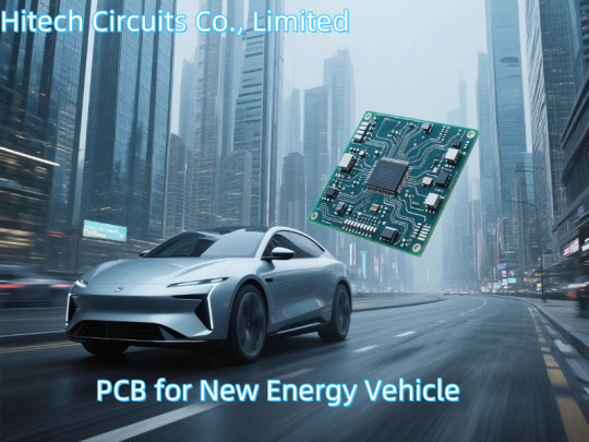
Common Printed Circuit Boards in New Energy Vehicles
As new energy vehicles handle high voltage and current, various PCB types are utilized to conduct and control electricity safely across functions:
Multi-layer PCBs 6-12+ layer boards employ complex internal circuitry to precisely transmit signals and power between electronic modules. More layers enable more robust connectivity.
Thick Copper PCBs Ultra-thick 2oz, 3oz and even 4oz copper reliably channels currents up to 400A+, applied for motor control and power conversion requiring stable high ampacity traces.
HDI PCBs High-density interconnect technology with microscopic vias and dense circuitry allows integrating more functionality and components in confined control units, saving space and weight.
Large-area PCBs Sprawling PCBs powering functions like body electronics and chassis controls enable more consolidated layouts and simplified connectivity.
At Hitech Circuits, we are a premier PCB manufacturer providing one-stop PCB fabrication and assembly services to meet the diverse needs across multiple industries. With years of experience and cutting-edge capabilities, we deliver high-quality, quick-turn PCB solutions tailored to each application’s unique requirements.
Our Core Expertise:
Wide range of PCB technologies: HDI, rigid-flex, RF/microwave, thermal boards, and more Advanced manufacturing processes: high-density interconnect, buried/blind vias and more Fast prototype to production cycle times Strong engineering support from quote to delivery High-reliability PCBs for demanding applications
Whether you need prototypes for new product development or high-volume PCB production, Hitech Circuits is your trusted partner.
1 note
·
View note
Text
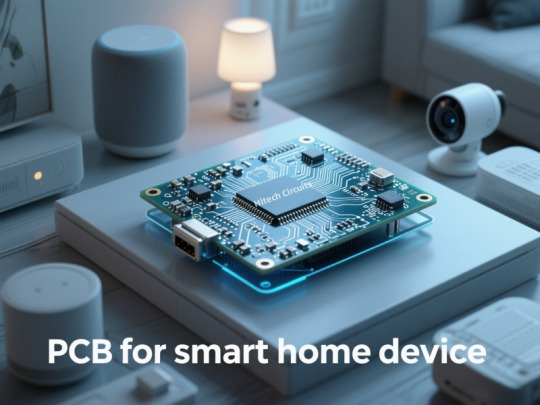
What Makes PCBs Vital in Smart Home Technology?
Smart home systems rely on various interconnected devices, from thermostats and lighting to voice assistants and security cameras. PCBs form the backbone of these devices, enabling their core functionalities.
Key roles of advanced PCB designs include:
Seamless Connectivity: With integrated wireless modules (Wi-Fi, Bluetooth, Zigbee), PCBs enable devices to communicate and function harmoniously in a smart home ecosystem.
Compactness and Flexibility: As devices shrink in size, modern PCBs are designed with multiple layers and flexible substrates, fitting neatly into small spaces without compromising performance.
Energy Efficiency: Smart homes demand energy-efficient solutions. PCBs with optimized layouts minimize power consumption, supporting eco-friendly and cost-effective operation.
Long-Term Durability: High-quality materials and robust designs ensure that smart devices remain operational under varying environmental conditions.
1 note
·
View note
Text

How is Aluminum PCB Made?
1. Material Selection: The primary material for Aluminum PCBs is an aluminum alloy, which acts as the base. This is paired with a thermally insulating layer and then a copper foil. The type of aluminum, insulating material, and copper thickness can vary based on the application.
2. Lamination: The layers are laminated together using heat and pressure. This ensures that the copper foil adheres well to the insulating layer, which in turn is bonded securely to the aluminum base.
3. Circuit Pattern Printing: Once laminated, the desired circuit pattern is printed onto the copper foil using a special ink. This ink acts as a protective barrier in the subsequent etching process.
4. Etching: The board is then subjected to an etching solution. This solution removes the exposed copper, leaving behind only the circuit pattern protected by the ink.
5. Drilling: Holes are drilled into the PCB for component leads or vias. This is done using precise CNC machines to ensure accuracy.
6. Surface Finish: To protect the exposed copper circuitry and improve solderability, a surface finish is applied. Common finishes include HASL (Hot Air Solder Leveling), ENIG (Electroless Nickel Immersion Gold), and OSP (Organic Solderability Preservatives).
7. Solder Mask Application: A solder mask is applied over the circuitry, leaving openings only where soldering will occur. This mask prevents accidental solder bridging during assembly.
8. Silkscreen Printing: For ease of assembly, reference designators and other important information are printed onto the PCB using ink.
9. Testing: Before shipping, the PCBs undergo electrical testing to ensure there are no shorts or open circuits.
10. Cutting and Profiling: The PCBs are then cut from the larger panel and profiled to the desired shape.
11. Final Inspection: A thorough visual inspection is done to ensure the PCB meets all quality standards.
The above process is a general overview, and specific processes will vary depending on the manufacturer and the intended application of the PCB.
0 notes
Text

High Frequency (HF) PCB is used to transmit electromagnetic waves in the frequency of GHz with minimal loses in the variety of applications, including mobile, microwave, radio frequency (RF) and high-speed design applications. Below is an example of a high frequency PCB:
Technical Parameters:
4 layers RF PCB
Material: Ro4350B+FR4 hybrid
Board thickness:1.6mm
Size:100mm*140mm
Immersion gold surface finished
Min.Width/Space: 0.152mm/0.175mm
Min. holes: 0.3mm
Application: Telecommunication
Hitech is a reliable high frequency RF pcb manufacturer in China. If you have related PCB needs, please feel free to contact us.
1 note
·
View note
Text

Hitech Circuits has extensive experience of PCBA manufacturing. We can provide the services of components sourcing and assembly. We have strict quality control for imcoming materials to ensure that the materials are genuine, good quality, and matched. Our factory has passed the ISO9001 and ISO14001 quality management system certification and the standard anti-static and dust-free production workshop meets the RoHS standard. Our equipment currently consists of 3 automatic SMT production lines, 2 DIP plug-in post-soldering lines. If you have inquiries about PCBA manufacturing, please feel free to contact us.
1 note
·
View note
Text

What are the differences between Flex and Rigid boards?
Flexible printed circuit boards are quite different than rigid boards:
Material; Rigid boards are typically made out of FR4 (glass-epoxy compounds) while flexible circuits are made from polyimide. There are cases when rigid boards are built with polyimide, but it isn't as common.
Coverlay; Flex pcbs either have a flexible mask or coverlay while rigid boards typically just use a solder mask. When a coverlay is used, the openings are routed, or laser cut. Then an adhesive (typically 1 or 2 mils thick) is used to adhere the coverlay to the flex.
Stiffeners; Flexible printed circuit boards typically use FR4 or polyimide stiffeners to stiffen specific non-flexing regions. Stiffeners are either laminated to the flex or adhered using a PSA (pressure sensitive adhesive). Rigid boards do not need stiffeners.
Permittivity; There is a wide range of relative permittivity (dielectric constants) for rigid board materials while flexible polyimide material is typically 3.4.
As a leading prototype-to-production flexible PCB manufacturer, we have flex and rigid-flex PCB capabilities that other companies can't compete with. As your flexible circuit supplier, you will be able to manufacture boards smaller line trace spaces and micro-vias. Consult with our team to help you determine what the optimal technologies are for your project's application. We also offer extremely fast quick turn flex circuit prototyping services. Contact us to learn full flexible capabilities.
1 note
·
View note
Text
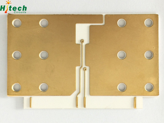
Ceramic Printed Circuit Manufacturing Processes and Technologies
Ceramic printed circuit board manufacturing processes can be categorised into four types: HTCC, LTCC, DBC and DPC.
The HTCC (High Temperature Co-fired Ceramic) process requires temperatures higher than 1300°C, but is quite expensive due to the choice of electrodes;
LTCC (Low Temperature Co-fired Ceramics) requires calcination at temperatures around 850°C but produces less accurate circuits with lower thermal conductivity in the final product;
DBC (Direct Bonded Ceramics) requires the formation of an alloy between the copper foil and the ceramic, and the calcination temperature must be tightly controlled in the 1065-1085°C temperature range. Since the thickness of the copper foil in the DBC method cannot be less than 3oz, the ratio between trace width and depth is limited in this type of ceramic printed circuit board.
DPC (direct plated ceramic) preparation methods include vacuum plating, wet plating, exposure plating, etching, and other processes, making the product relatively expensive. In addition, DPC ceramic circuit boards require laser cutting, which cannot be accurately processed by conventional drilling, milling, or punching machines, and thus laser cutting provides more precise bond strength and trace width.
Hitech Circuits is a trustworthy Ceramic PCB manufacturer in China. If you have related PCB needs, please feel free to contact Us.
1 note
·
View note
Text

Looking for high-reliability FPC or Rigid-Flex PCBs? At Hitech Circuits, we deliver precision, performance, and speed!
Up to 10-layer Rigid-Flex & 4-layer FPC Min. trace/space: 0.051mm / 0.076mm Min. drill hole: 0.20mm Base copper: 1/3oz – 2oz Surface finishes: ENIG, OSP, Immersion Tin & Carbon Ink Flame rating: 94V-0 | Dielectric strength: AC500V
Fast prototyping. Consistent quality. Global service. Contact us today to get started! https://hitechcircuits.com/pcb-products/flexible-pcb/
0 notes
Text

Looking for a high-precision custom PCB manufacturer?
At Hitech Circuits, we specialize in advanced multilayer PCB prototyping, tailored to your unique requirements.
Trace/space down to 3mil (0.075mm) Local fine-line spacing as tight as 2.5mil Impedance control within ±8% Hole tolerance up to ±0.05mm
Let us turn your complex PCB designs into reality. Get in touch today! hitechcircuits.com
1 note
·
View note
Text

Hitech’s Capabilities for Copper Based Substrate Manufacturing
Looking for high-performance metal core PCBs with exceptional thermal conductivity and precision engineering? Hitech Circuits has you covered with expert prototyping and small-batch production!
Key Capabilities: • Single / Double side PCBs, up to 1500 × 480 mm • Board thickness: 0.2mm–4.5mm, copper: 18–240μm • Min. hole size: 0.2 mm, hole position tolerance: ±0.075 mm • Fine punching: round holes ≥1.0mm, square slots ≥0.8×0.8mm • V-CUT board thickness: 0.6–3.2mm, angle deviation: ±0.5°
Thermal Performance: • Copper base up to 401 W/(m·K) • Insulation layer up to 38 W/(m·K) • Thermoelectric separation tech: up to 398 W/(m·K) — perfect for ultra-high heat flux designs
Precision & Finish: • Impedance control: within ±8% • Surface finishes: ENIG, ENEPIG, HASL, OSP, and more • Solder mask colors: Green, White, Blue, Red, Matte Black
Production & Delivery: • Capacity: 10,000 m²/month • Lead time: 5–7 days (prototype), 10–14 days (mass production)
Let's bring your thermal-critical projects to life — fast and reliably. Contact us now for a quote! https://www.htmpcb.com/metal-core-pcb-c-10.html
1 note
·
View note
Text

Hitech Circuits – Your Trusted LED PCB Manufacturer in China
When it comes to high-performance LED PCB solutions, Hitech Circuits stands as your reliable and innovative manufacturing partner. With years of expertise and a strong supply chain, we are fully equipped to support your LED lighting projects—from prototype to production—with speed, precision, and cost-effectiveness.
Premium Materials, Tailored for Performance
We maintain a full inventory of top-tier LED PCB base materials to meet your most demanding applications, including: Totking, Bergquist, Laird, Kinwong, Doosan, ITEQ, Shengyi, Polytronics, Arlon, Ventec and more. Looking to lower costs without compromising quality? We can also recommend cost-effective local aluminum base suppliers that are tested and proven in real-world performance.
Request our LED PCB Materials List for more details—or contact our sales team directly for tailored suggestions.
What Makes Hitech Circuits Your Go-To LED PCB Supplier?
✅ 1–6 Layer Aluminum & Copper Base LED PCBs ✅ 24/7 Live Sales & Tech Support – Instant responses within 2 hours ✅ No MOQ – We welcome all orders, from single-piece prototypes to large-scale runs ✅ 24-Hour Rapid Prototyping Services ✅ Expert Engineering Support – From stackup design to thermal management optimization
Whether you’re designing LED bulbs, strip lights, automotive lighting, or high-power industrial applications, Hitech Circuits delivers precision-crafted PCBs with excellent heat dissipation, high reliability, and flexible customization options.
Global Service. Local Expertise.
With customers across Europe, North America, and Asia, our team understands your project needs and can speak your language—both technically and culturally. From inquiry to delivery, we provide end-to-end service with transparency and care.
Let’s start your next LED PCB project today! Reach out for a fast quote or free technical consultation.
hitechcircuits.com [email protected]
#LEDPCB #PCBSupplier #AluminumPCB #CopperCorePCB #HighPowerPCB #PCBPrototype #HitechCircuits #ThermalManagement #ChinaPCBFactory
#LEDPCB#PCBSupplier#AluminumPCB#CopperCorePCB#HighPowerPCB#PCBPrototype#HitechCircuits#ThermalManagement#ChinaPCBFactory
1 note
·
View note
Text

Hitech Circuits—Your Reliable Supplier for Premium PCB Assembly
At Hitech Circuits, we specialize in high-efficiency, high-precision surface mount technology (SMT) assembly, delivering unmatched capacity and quality for your PCB projects.
Our Capabilities:
1. Massive Daily Output
1 Million+ Components Placed Daily**: Powered by fully automated SMT lines (e.g., Fuji NXT, Siemens SIPLACE) and high-speed pick-and-place systems, we ensure rapid production scaling for both prototypes and bulk orders.
2. Advanced Packaging Expertise
QFN/BGA Mastery: Our precision equipment handles ultra-fine-pitch components, including QFN (0.3mm pitch) and BGA (down to 0.2mm ball diameter), with 99.99% placement accuracy.
X-Ray Inspection: 100% in-line X-ray verification for BGA solder joints, voids, and alignment defects, ensuring zero hidden faults.
3. End-to-End Quality Control
AOI + SPI Integration: Automated Optical Inspection (AOI) and Solder Paste Inspection (SPI) at every stage.
IPC-A-610/612 Compliance: Certified processes for mission-critical applications.
Why Choose Us?
Speed-to-Market: 48-hour prototype turnaround & 10-day mass production cycles.
Flexible MOQs: Support for small-batch R&D to 100k+ volume orders.
Global Material Sourcing: Access to a vetted network of component suppliers, reducing lead times.
Contact Us Today!
Let’s optimize your PCB assembly with speed, precision, and reliability.
Email:[email protected]
Tel & Whatsapp: +86-180333061378
Location: Building C, Suojia Technology Park, Hangcheng, Xixiang, Shenzhen, Guangdong, China
Authority certification: we're fully ISO9001:2015, ISO14001:2015 , UL (E354070) and RoHS certificated. You can reply on us for custom PCB production and Electronic assembly.
1 note
·
View note
Text

Heavy Copper Core PCB with Depth Control Slot
Layer: 6L
Panelization: 6-in-1 panel
Unit Size:40*80mm
Panel Size:150*193mm
Material: FR-4 Tg170℃ S1000-2
Board thickness: 2.40mm
Surface finished: ENIG
Copper thickness: 4 oz
1 note
·
View note