
A long journey into electronics starts with a single solder
Don't wanna be here? Send us removal request.
Statistics
We looked inside some of the posts by joesimeon-blog and here's what we found interesting.
Average Info
Notes Per Post
0
Likes Per Post
0
Reblog Per Post
0
Reply Per Post
0
Time Between Posts
1 day
Number of Posts By Type
Text
8
Last Seen Tumblr Blogs


Fun Fact
After the announcement of the deal with Yahoo!, there were 170K signatures of unhappy Tumblr users petitioning to prevent the sale in 2013.
Text
Computer Systems Sample Code - Sample Sort
This section will demonstrate some sampled code for 3302ENG Computer System Lab which will be discussed below.
Parallel sort assignment
Question 1
Write a program that performs a sample sort on a dataset that you create. The dataset is a space delimited list of integers between 0 and 1000. The program should open a file called dataset.txt which contains the data to be sorted. The number of bins used is your choice. The program should also time the length of time taken to complete the sort.
Hints: The timing functions can easily be found in any slightly advanced C programming textbook or website. Also make sure that you use a large enough dataset to get a meaningful time.
Question 2
Modify Q1 so that it uses threads to perform a parallel sample sort.
Question 3
The aim of part 3 is to determine the effect of increasing the number of threads on the time taken to perform the parallel sort. This will be demonstrated by plotting a graph of the average time for the sort versus the number of threads used.
You should choose the number of threads so that range is 1 <= number of threads <= 10.
Repeat this procedure 3 times and calculate the average taken time for the different number of threads.
Plot the graph of the average time for the sort vs the number of threads used.
Write down the processor type and the number of cores for the computer that you used to perform this question.
Explain the graph.
Analysis of the implemented sample sort

Figure: Average time taken for each # of thread used in the parallel programming of a sample sort used in conjuncture with a Bucket Sort via multithreading.
The increasing of sorting ranges via the addition of another thread to sort a particular range of integers shows that certain thread numbers (using parallel sorting of 2 – 3) could be beneficial with dips in 5 and 7 where the larger of the resources being chewed up by the program from the system is happening around 8 to 10 threads.
The higher peaks happening at thread numbers 4 and 6 could be from a range for one bucket containing a majority of the randomised data, the distribution could be held entirely by accident from a poor sampling algorithm, decreasing the overall time can be achieved by re-evaluating how a random sample of the whole dataset is obtained, post sorting and acquiring splitters from the sorted random sample could help distribute the whole dataset evenly amongst the buckets (threads).
Code
Github link to Generating data to sample C File
The C File will contain the code to generate the needed data for the sampling algorithim.
Github link to Question 1 C File
This C File will contain the code for sample sorting the generated data Txt File - the code itself is different from the next C File which is a combination of Question 1 and Question 2, the main difference within this code is that the sorting algorithim will examine the amount of the pieces of data and resize for an appropriate amount of buckets to be used to sort the amount of data, it’s aim is to stay relatively in the low-middle section of the thread numbers such as (2 - 5).
Github link to Question 1 Question 2 C File
Alternative C File at Github
This C File will contain the code for sample sorting the generated data Txt File - the code itself will sort data at the number of threads that the user chooses. The alternative file is the same code with the removal of the printed to terminal data positions as a measure to examine whether it is working the way it should be.
Issues occurred and possible solution
Problem 1:
An occurrance was during the accessing of critical code, which content of first thread will be mixed by the content of the nth thread.
Possible solutions for problem 1:
Thread locking the critical code and allowing each thread to enter and submit the data at the appropriate position in the array of sorted data, which means keeping track of where it is between shared memory between threads.
Implemented solution for problem 1:
Mutex locking, conditional numbers with mutex condition broadcasting and waiting so that thread 1 will access the critical code sections and will allow the data to be inserted increasing the conditional number up until the nth thread, for this section of the code the parallel programming because serial however it is not destructive.
Problem 2:
The sorting of the random data resulted in one bucket taking most of the load of the data, when each bucket was given a number range.
Possible solutions for problem 2:
Eliminating the use of the number ranged buckets and give each bucket a random number of elements to be sorted with in perspective bucket and allowing a simple mutex lock and let each thread insertion sort each number - it will elminiate overhead of the storage for a slower time.
Implemented solution for problem 2:
A solution has yet to be implemented.
Revision
This is the revision of the code to make it a little more efficient.
0 notes
Text
Practical Electronics Project [SUBMISSION]
Function Generator
by Joseph Simeon, s2966176, [email protected]
Jon Holder, s2717118, [email protected]
Introduction
This document will report on the construction, design, and analysis of a function generator that is created for 3302ENG – Practical Electronics course at Griffith University. This report will detail the project lifecycle through discussion of the requirements, market analysis of the board, design and testing phases of the board, user manual and concluding analysis of the project overall.
A function generator is an important piece of electronic laboratory equipment which helps in the design and testing of electronic equipment. Circuits require reliable signal generation which will simulate normal operation of the circuit, controllable signal from low to high frequencies as well as low to high voltage ranges makes the function generator more versatile and invaluable for electronic analysis in a controlled environment.
Stated in ‘Function generator and arbitrary waveform generator guidebook’ by D. Peterson and B&K Precision that function generators are used where stable and repeatable stimulus signals are needed with common uses as:
Research and development
Stimulus/response testing
Frequency response characterisation
In-circuit signal injection
And used by:
Education institutions
Electronics and electrical equipment repair businesses
Electronic hobbyists
Function generators of today provide a variety of signal creation such as:
Waveforms: Pulse, square, triangle, sine, sawtooth.
Variable frequency: less than 1 Hz to (up to at least) 1 MHz
Adjustable DC offset
Variable amplitude depending on the circuit
Extra features
PROJECT SCOPE
The scope of the project was to design, create and present a printed circuit board of a chosen project within a time-frame of 4/5 weeks (Griffith University’s semester 1 week 7 to week 11), the project that was chosen and submitted by this group was a function generator. This section will discuss the Project scope – the timeframe, requirements, submitted design and the changes of the design post-submission.
Requirements
The requirements for the project were provided by the course convener via document given called 2018 Project Exemplars, within this document the function generator was chosen as an exemplar because the project met the requirement of analogue circuit complexity, mature circuits (i.e. well-tested) and the components to construct the circuits are readily available in the lab.
The circuit should produce a variety of waves – sine, triangle and pulse with adjustable amplitude and frequency. The project is broken down into stages where the first stage is an astable multivibrator, the second and third stage are both integrators. The first stage will produce square wave and thus the second and third being integrators will output triangle and sine respectively. For this project the minimum frequency is set to be 5 kHz, an amplifier will be needed to adjust the amplitude of the output signal. The demonstration for the three waveforms on the oscilloscope.
Submitted design
The design was submitted in which the function generator would generate the three waveforms required in the project exemplar however the frequency minimum was set to 5kHz with no higher limit frequency to allow for deciding the upper limit later through the development cycle, it was submitted with adjustable amplitude with no value range as the railed voltage value of V+ and V- were not chosen at the time.

Figure 1. 'Circuit proposal' Figure from 3301ENG project submission Power Point.
The values for each resistor and capacitors were not used as the values had not be calculated yet because the design and testing phase in our project had not begun as a group due to multiple university commitments leaving not a lot of time during the submission phase of the project. A later submission phase might have resolved issues of not having limits set among the circuit proposal figure seen above.
Post-review changes
These changes occurred after the review of the submitted design and before the design and testing phase, this report will reflect on all changes that occurred through-out the process of creating of the function generator later in the document.
Before the design and testing process started, 555-timer was decided to be implemented instead of the op-amp for the first stage – astable multivibrator due to an easier implementation and calculation as well as keeping a stable 50% duty cycle. The frequency range that was set for the 555-timer was to be set to 5kHz to 200kHz however due to the 555-timer not being stable after a frequency of 50kHz thus another frequency was decided on a max frequency of 20Khz and min frequency of 20Hz.
MARKET ANALYSIS
This section will discuss the pricing of current commercially sold function generators and compare the features that each price range holds over the other; the analysis of the commercially available products will be compared against the prototype that was created for this project.
Low-end price range
As an example of a low-end price range function generator within Australia, the SFG-1013 is sold at $199.00 from EMONA instruments. The specifications of the SFG-series 1000 has:
Output function: sine, square, triangle, TTL.
Frequency range of 0.1Hz – 3MHz for sine and square
Frequency range of 0.1 – 1MHz for triangle
Resolution: 0.1Hz maximum
Amplitude range: 10Vp-p
Resistance load of 50 ohm at 10% tolerance
Duty control range 25% to 75%
6-digit LED display
High-end price range
As an example of a high-end price range function generator within Australia, the TG5011 is sold at $1906.00 from EMONA instruments. The specifications of the TG-5011:
Output function: sine, exponential rise, logarithmic rise, DC, triangle, square.
Frequency range of 1uHz to 50MHz for sine and square
Frequency range of 1uHz to 500kHz for triangle
Frequency range of 500uHz to 12.5MHz for pulse
Resolution: 1uHz or 14-digit
Amplitude range: 20mV to 20Vp-p open circuit and 10mV to 10Vp-p into 50 ohm.
Resistance load of 50 ohm
Variable duty cycle for certain frequency ranges
High resolution LCD
Gaussian white noise
Modulation: AM, FM PM, PWM, FSK, Triggered burst, Gated, Sweep, Trigger Generator.
Interfaces: USB, LAN, USB flash drive
Inputs: Trig in, external modulation input, ref clock input.
Prototype
The prototype costing is at base prices of single components and not at bulk sale allowing to know the maximum possible price of the board, the components will be at Australian market price however the price of the board will be sourced from a Chinese competitor within the industry since Australian prices for the boards to be made are expensive:

Table 1. Cost analysis of the current prototype
The prototype designed and built during this project lifecycle was built with these possible functions:
Output function: sine, triangle, square.
Frequency range of 200Hz to 20kHz for all waveforms
Amplitude range of 4Vp-p
Fixed duty cycle of 50%
Ability to be run of a 9V battery
At the current price of the prototype with the cost analysis being a one-off production without any bulk purchases of components and PCB, the ratio of functionality and cost does not directly compete with current low-end competitive prices at commercial sale.
Prototype MK-II
The prototype costing is at base prices of single components and not at bulk sale, allowing calculation if the maximum possible price of the board, the components will be at Australian market price however the price of the board will be sourced from a Chinese competitor within the industry since Australian prices for the boards to be made are expensive:

Table 2. Cost analysis of the current prototype - MKII
The prototype designed and built during this project lifecycle was built with these possible functions:
Output function: sine, triangle, square.
Frequency range of 200Hz to 20kHz for all waveforms
Amplitude range of 4Vp-p
Fixed duty cycle of 50%
Ability to be run of a 9V battery
At the new price of the prototype (MKII) with the cost analysis being a one-off production without any bulk purchases of components and PCB, the ratio of functionality and cost does not directly compete with current low-end competitive prices at commercial sale even with a $8 dollar AUD price down, bulk sales of component prices in China could compete.
Out-sourced Chinese market
This is the price of the entire board with the Australian price value for the components within a leading manufacturer of electronic components – at the price of a board costing one-off production and the price of the board at a bulk production of 1000 boards:

Table 3. Chinese manufactured out-sourced costs of one-production and 1000 production component price per board
By out-sourcing the component acquirement to China as well, the cost to purchase the components have dropped in both one-off production and 1,000 productions to that of over x3 less and over x7 less respectively in terms of cost cutting resulting in a board production that could compete with low-end market for price if the function generator prototype could produce higher frequency ranges.
DESIGN AND TESTING PROCESS
Design of the project was broken down into modules which were designed separately before being bought together as a single unit for testing and packaging. The design was broken down into the following modules:
Power supply stabilising circuit.
555 -timer circuit outputting a 50% duty cycle square wave.
Integrator 1- Square wave input, Triangle wave output.
Integrator 2- Triangle wave input, sine wave output.
Buffer circuits
Amplifier
Each of the above modules were individually designed and simulated with the use of circuitlab.com before being constructed and tested with an existing oscilloscope and function generator DS0-X 2002A from Agilent Technologies.
Two function generator prototypes have been developed from the above modules, both will be discussed below.
Power stablising circuit
0 notes
Text
Practical Electronics Project [REQUIREMENTS]
Task description:
Students will work in groups of two to complete a circuit design project from start to finish, moving through the phases of:
Definition of project concept that is started during the preliminary circuit design review
Electronic circuit design that is started during the preliminary circuit design review
Bread board prototyping of the proposed circuit0
Design of PCB for the proposed circuit
Assembly of the circuit on the PCB, once it is fabricated
Testing methodology that is geared towards the targeted application
Demonstration of the circuit meeting the design specifications
Documentation of the project in a formal written report
Ordering components and maximum cost:
You are strongly advised to use the components that have been provided when you are doing the intro lab. You are allowed to order additional components using the component order form, which requires approval from the lab demonstrator. The total cost should not exceed AUD 20. Be aware that there will be a delay (lead time) of few weeks to receive your order. For speedier alternative, you could purchase these components yourself at electronics stores such as Jaycar (https://www.jaycar.com.au) with no cost limitation. However, the school will not refund this purchase.
Schedule:
Week 6: After receiving and addressing (if applicable) the written feedback that was given by the convenor during the preliminary circuit design review, you should check the list of components in your armoury. The missing components should be obtained. Please see details under “Ordering Components and Maximum Cost”.
Week 7 to Week 10: First, you will construct and test your proposed circuits on the breadboard. Then, you should design the PCB and submit it fabrication. Please be reminded that the PCB will be made in batches. Therefore, there is a turnaround time to get your PCB back from the workshop. Once the PCB is fabricated, you must assemble and solder the components on it, and perform the final testing.
Week 11: You must demonstrate the output of your project in front of the teaching team during the scheduled laboratory session. Then, the written report must be deposited at L@G by 25 May 2017 at 11:59 PM. Please submit one report per group. The guidelines for writing this document are provided in the next section. Please be aware that the teaching team uses Turnitin to detect plagiarism.
Week 12-15: The teaching team will read all the reports and conduct moderation meeting to finalize the marks that will be allocated to each group. The total marks (out of 50) will be released at the MarkCentre before the end-of-semester exam. The marking breakdown and the comments will be emailed to each group.
Guidelines for writing the report:
The report must include the following chapters: (1) Introduction; (2) Market analysis; (3) Design and simulation (if applicable) methodologies; (4) Testing methodologies and results; (5) Analysis; (6) Conclusion; and references and appendices.
Chapter 1 should briefly introduce the project, its objectives and outcomes. It must also include a statement clearly outlining the activities completed by each group member.
Chapter 2 must clearly specify the intended applications of your circuits and list the commercial competitors. You are required to make arguments to trump your competitors. While different projects will require different emphasis, the following factors can be addressed: retail price, offered functionalities, technical risks, compliance and standards, ease of installation and maintenances, ergonomics, environmental, social and ethical impacts etc.
Chapter 3 must emphasize on the design thought process. This is your primary avenue to document your creative design and troubleshooting efforts to achieve what you propose in the specification, despite all the technical and non-technical challenges.
Chapter 4 must justify the choice of chosen methods for the intended applications. You must be able to demonstrate the functionalities of each module and then the overall project. Some key results should be presented in figures, and they must be labelled properly. The high volume data should be summarized in a table.
Chapter 5 must document the performance of your project using standard parameters that can be compared with the competing products (refer to chapter 2). You must also supply a high resolution photograph of the final product, with clear labels of the individual models.
Chapter 6 should highlight any insights and interesting lessons that you have learnt after completing this project.
Please use IEEE format for the referencing and citation
0 notes
Text
Microprocessor Techniques Project [REVISION]
This section is to do with how I want to extend this project further post-submission, how it will be done and the results within doing so.
Create a user interface application
Process the data more efficiently
Possible use of all actionable interrupts
Continuous stream of data
Capturing tool
0 notes
Text
Microprocessor Techniques Project [SUBMISSION]
DIGITAL STORAGE OSCILLOSCOPE USING A TIVA C SERIES LAUNCHPAD
by Joseph Simeon, s2955176, [email protected]
Introduction
Tiva C Series LaunchPad (TM4C123G) is an in-expensive single-board microcontroller evaluation platform for the ARM Cortex-M4F created by the company Texas Instruments. This project will be using Texas Instruments Tiva C Series microcontroller in creating a Digital Storage Oscilloscope (DSO); DSO is an electronic test instrument that allows to observe signal voltages, it is analysing the input signals digitally instead of analogue displaying the results in graphic form utilising an x-y co-ordinate system approach to data distribution.
The aim of this project is to create a digital oscilloscope using the Tiva C Series LaunchPad programmed specifically with embedded C-Language within a time-frame of 25th August 2017 to 21st September 2017. The digital oscilloscope will be displayed in graphical form in the terminal using special ANSI escape characters, as well as the parameters will be controlled via the terminal using certain keyboard buttons corresponding with actions such as:

A graphical representation will be displayed on the computer using the terminal which will be where these actions can be implemented. The short-term goal is a minimum graphical design of the graph that will be displayed, where-as a long-term goal would be a deeper design of the graph and friendlier visual in terms of analysing the data presented as well as incorporation of a physical design such as a user-friendly enclosure.
The project's greatest challenge is the setup of the ADC to receive data from the pin and relating the readings over a period into graphical representation using ANSI within the terminal, the more user friendly and better design requires more in-depth knowledge to code a better interface to interact with the user, the physical designing of the connection that will attach voltage signal to wires that will connect the to the observing pin will be minimal first and later if time allows will create a better design to incorporate user friendly interaction.
METHODS
Features
Board specific features

Tiva C Series LaunchPad (TM4C123G) Evaluation Board
Image reference “Tiva C Series TM4C123G LaunchPad Evaluation Board – User’s Guide by Texas Instrument, 2013”.
Tiva TM4C123GH6PMI microcontroller – 32-bit ARM Cortex M4-based microcontroller
Motion control PWM
256 kB Flash memory, 32 kB SRAM, and 80MHz operation
16 MHz crystal – microcontroller main internal clock
External 32.768 kHz crystal – for hibernation module
Internal PLL – for frequencies up to 80 MHz
USB 2.0 device interface with micro-USB connector
RGB LED
2 programmable user switches/buttons
I/O available via headers
On-board Tiva In-Circuit Debug Interface (ICDI)
Switch-selectable power sources (USB, ICDI)
Reset switch
Use of ARM Thumb-compatible Thumb-2 instruction set
(David Rowlands, 2017)
Utilised features

Features of the board represented by the different subsystems that exist.
Image reference: “Embedded systems: Introduction to the ARM Cortex™-M microcontrollers, Volume 1 by Jonathan Valvano, 2012”.
The subsystems that will be used in the project of creating a DSO will be:
UART0 activated on pins A [0, 1]
ADC0 activated on pin E [3]
TIMER0 activated via ADC
UART stands for Universal Asynchronous Receiver-Transmitter, the subsystem will be used for serial communication between the board and the computer through a terminal, transmitting and receiving data – this project will be using UART0 which uses General Purpose Input-Output (GPIO) Port A, Pin 0 & Pin 1.
ADC stands for Analogue-Digital Converter, the subsystem that uses an electronic process to receive varying signal in voltage (analogue) and converts the signal to a digital level. The digital levels are determined by how many bits the analogue signal will be digested into, such as if the signal is being digested by 12-bit than the digital level will be between the limits of 0 to 4095, where 4095 would reflect 3.3 Volts (V) because the limits of the Tiva is between its lowest voltage of Ground (GND)\0 V and Supply voltage (Vcc) \ 3.3 V analogue signals that move below or above the limited voltages will be truncated to fit within the boards limitation. The project will be using ADC0 which uses GPIO Port E, Pin 3.
General Purpose Timers (TIMER) is a subsystem of programmable timers that are connected to GPIO pins, it will count down and trigger the ADC once zero is reached, this will relate to a frequency as which the ADC is being triggered. The project will be using TIMER0 which will be activated on the ADC Pin and will connect to the ADC triggering.
Hardware
Two set ups were used as the items used in the laboratory could not be replicated exactly outside the lab when the project was worked on during non-laboratory allocated time. The list of hardware during these times are:
General Equipment
The general equipment will be used in laboratory and non-laboratory testing.
Tiva C Series TM4C123G LaunchPad
Breadboard
Female to Male or Male to Male pins
Laboratory Specific
The laboratory equipment will be used only in the laboratory – an older model Oscilloscope (DSO/CRO) which does not have a wave generator will need a function generator where-as later models will have this feature.
Function generator
Digital Storage Oscilloscope
Non-laboratory Specific
The non-laboratory equipment will be used to test the project outside of laboratory allocated time.
Potentiometer (Varying resistor)
Design
Complex algorithms
The most complex parts of this experiment are the setting up of the UART and ADC with TIMER along with each subsystem’s subtasks and manipulating the data received from the ADC’s Analogue Input Pin to feed into specific functions such as creating the DSO graph as well as signal information that can be accessed before the calling of the graph output. Main algorithms:
Subsystems with off-task
Manipulating data
Signal information via user interface
DSO output graph
Main blocks & sub-tasks & off-tasks
Subsystems that are not being manipulated by the prepared functions by TivaWare will needed to be accessed via direct register set-up using embedded C, even though Assembly (ASM) direct register set-up takes more lines of code, both can yield errors when via destructive masks or not turning the right bits within the register, within the main block of setting up the registers, off-tasks that utilise the set-up will be included though they are not subtasks but are needed tasks that rely on a perfect set-up.
The manipulating of ADC data received will be given to the DSO output graph after it has been manipulated to fit within the graph size, the data received from the ADC will also be manipulated and fed to the user interface that will allow the user to see information before moving onto the output graph.
Subsystem
UART initialisation
GPIO initialisation for UART
Receiving characters
Transmitting characters
Printing strings via UART transmitting of characters
ADC initialisation
GPIO initialisation for ADC
TIMER initialisation for ADC
Frequency changes to TIMER via preload change
Transmitting of data via ADC
Main-code
User interface
Pre-defined set-up for graph using key and actions
Manipulating data to export values
Graphing of signal
Manipulating data to represent values
Simplified & complex project design
The simplified design in the project is to create a user interface that allows the person to implement predefined actions before the screen refreshes to two different graphing outputs, one being a single measurement and the other being a repeating measurement for 5 seconds. The physical aspect of the project will be within the style of just pins (female to male or male to male) connected to the Tiva board either directly to the CRO/DSO/Wave generator or via a variable resistor using a breadboard.
The complex design in the project is to create a user interface that sits off-side to the graph, the main feature of the project is an already set graph and at the bottom people can control the features along with continuous fresh readings of the instantaneous voltage and minimum and maximum voltages, with more ability for higher sampling rates, the graph will run at a single measurement or a repeating measurement however adjustments can be made within the same window meaning that at no point will the window refresh but only the values themselves in real time. The physical aspect of the project will be for a more complex design is an enclosure that the Tiva will sit in an enclosure with either a breadboard or pins sticking out of the enclosure to be attached onto it, with enough time also a short instructional pictogram to show how to effectively use it.
SOLUTION
Block diagram of system structure

Block diagram representing the system and its connections between the ‘moving’ parts.
Ciruit diagram

Circuit diagram showing Tiva Board’s connection via ADC Ain0 with testing connections to a variable resistor and signal generator.
Subsystem set-up

The system clock is enabled for ADC0, Port E and TIMER0 – legacy registers were used for ADC and TIMER, delays were used afterwards to force the board to wait and stabilised.

GPIO set-up for Port E clearing all digital settings and input settings to enable alternative select and analogue mode.
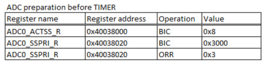
ADC0 – Sequencer 3 (SS3) is disabled and priority of SS3 is made highest while priority of SS0 is made low.

The TIMER0A is disabled to be configured for a periodic triggering to the ADC that has a prescaler of 255 with an arbtriary value of 255 within the preload which will be changed when the program starts, match value is zero for no use of duty cycle.

SS3 is set to timer trigger as well as sampling control bits through source Ain0 then both TIMER0A and SS3 are enabled to be used.

UART0 is disabled so transmitting and receiving data can be set and specified parameters for baud rate, word length, parity, stop bit are set as well.

GPIO for UART0 is set with alternative select enabled, digital enabled and the port control numbers to specific the alternative function (U0Rx, U0Tx – UART0) with enabling UART.
Algorithmic flowchart

Algorithm of the main code processes the actions via user input, the key and actions are explained in the introduction of the report.

Action algorithm that results in the user choosing specified actions before outputting the actions to the construction of the graph.

Smaller algorithms from the action algorithm revealing how some of the processing works.
Testing methodology
The testing of correct operation of subsystems were a step-by-step activation via the debugger built within Keil and ultimately via the UART testing that the terminal linking to the UART’s specified baud rate, word length, parity, stop bit and flow control (921600, 8-bit, odd parity, 2-bit stop, no flow control) and receiving and transmitting characters via an echo loop.
The ADC set-up was activated slowly by first through activating just the ADC0 and then testing the debug, then GPIO and then finally TIMER, once the debug showed that the set-up was not being caught in a loop, data retrieval was testing using a potentiometer via Port E Pin 3, ADC data was printed straight to screen unprocessed showing indeed that the step values was from 0 to 4095. Each function within the program was tested via known variables and hardcoding static values that would be used in the program, the results needed were displayed straight to screen.
User manual

Circuit diagram.
Upon successfully connecting your Tiva C Series “DSO” LaunchPad to the computer and ensured that component that will be tested is attached to the appropriate pins via the circuit diagram, open Tera Term and begin to set-up the serial port to the specifications below:

Tera Term specifications.
When the specifications is correct you will be given an input list of keyboard buttons and the actions that will occur; below is the list of buttons to press as well as the outputs you will be expected to see, leading up to the predefine values for the graph output and the two different types of graph output that the user can choose from – single measurement or measurement over 5 seconds.

Listed keys and actions.

Single measurement graph output.

5 second measurement graph output.
Evaluation
The project in which a Tiva C series TM4C123G LaunchPad Evaluation Board is used to create a Digital Storage Oscilloscope (DSO) is successful with resulting in a plotting of the signal that is being set once the user has set parameters within the user interface that is separated from both graph outputs while using a simple physical project design of using pins directly connecting to the Tiva board to the CRO/DSO via allotted laboratory time while outside the laboratory the simple connection was via a breadboard and a variable resistors.
Due to the project being within a time-frame, not enough time could have been utilised to create an enclosure for the Tiva board, the code for the complex project was not managed to be implemented however the user interface of the graph was recreated to provide better visual representation than the simplified white.
Problems have occurred during the creation of the project which will be explained in the discussion section of this report however although most problems have been solved or altered; a major on-going problem which due to the time-sensitive nature of this project, the ADC happens to halve all input values through the Ain0 pin which will also be discussed.
Discussion
The problems that have occurred during the project is within the initialisation of the ADC, during the debug testing it would move through the ADC without a problem however the input pin’s ADC data value was pulling zero values to the screen, upon inspection of the registers and content it was revealed that the preload register was set to a value that was outside the parameter causing the register to wrap around in value to zero thus ADC not triggering at all.
Embedded C has functions that don’t work or are left as a skeleton that needs to be filled in, one such example is the ‘printf()’ function that exists within the ‘stdio.h’ header that is left as a skeleton ready to be filled in with self-created functions that are known as ‘fgets()’, ‘fgetc()’ and ‘ferror()’. These functions that need to be created in order for ‘printf()’ to work however even with the self-created functions the function still did not work thus using a ‘out_char’ function that outputs a character via UART data register is used in a for loop until length of the string is reached, the starting memory address of the string is given to the print string function using a pointer to the start of the string wanted to be printed. Due to the time-frame and the set back with the direct register set-up taking longer than expected the complex project milestones could not be implemented such as the single page graph with user commands and dynamic values that would be constantly updated upon user selection or while the graph was in use with either single measurement or set time.
A major on-going issue is that the ADC is halving the input numbers being read by the pin, the registers are been looked through and the generator signal was tested by the Tiva board and by the CRO in which was generated by the CRO so evaluated possible problems, the registers although have been looked through intensely via the datasheet available for the TM4C123G – the only solutions thus far is debugging and ultimately re-writing the functions that create the graph as well as re-evaluating the direct register set-up or re-building the project from the ground up using the previous code as a frame-network possibly re-creating more efficient ways of handling the task.
Conlusion
Although the project is completed and complex project model has not been implemented, with the exception of the ADC halving values being sent to the pin and not allowing the solution of hard-coding the project does indeed project a input signal at different frequencies via the user input as predefined values before analysing the signal through a display of the graph output, room for improvement of the project overall as how it could work and how it could look could have been implemented given more time of excess of a week however the dates were already set with no flexibility.
References
Texas Instruments, 2013, Tiva C Series TM4C123G Evaluation Board – User’s Guide, Texas Instruments Incorporated, Dallas, Texas 75265. Literature Number: SPMU296 David Rowlands, 2017, 1B) Introduction to uCs - 2303ENG Lecture Notes, Griffith School of Engineering, Griffith University. David Rowlands, 2017, 6B) General Purpose Timers - 2303ENG Lecture Notes, Griffith School of Engineering, Griffith University. David Rowlands, 2017, Analog Signals - 2303ENG Lecture Notes, Griffith School of Engineering, Griffith University.
APPENDIX
main.c
Github link to the C source file
These links are not the C source file however they are needed for the project.
Github link to the Startup.s file
Github link to the uVision project file
Github link to the register Header file
uart.c
Github link to the UART C & Header file
adc.c
Github link to the ADC C & Header file
functions.c
Github link to the Functions C & Header file
graph.c
Github link to the Graphc C & Header file
0 notes
Text
Microprocessor Techniques Project [REQUIREMENTS]
Introduction and Background
C language is commonly used to program microcontrollers. This project is based upon using parts of previous experiments and topics covered in lectures, along with information from datasheets and external sources, to design and implement an embedded system utilizing the Tiva microcontroller.
Information and Hints
Write programs to be nondestructive.
Determine the main blocks of your system, then break down each block into smaller and smaller parts (top-down design method).
Plan how to test the correct operation of each part.
Ensure each part of the system is working before bringing together and attempting completed system testing.
Requirements
The final project requires student to design, implement and test a complete embedded system, utilizing knowledge and skills developed throughout the course. Students may choose either a provided project, or may choose a project of their own. It is up to the student to ensure that hardware required for their project is available.
For the chosen project, you need to begin by compiling the system requirements. This should describe the system you intend to design, and identify the main components of the system. This should also identify the features for a basic version of the project, and features that will be added to improve the system as time allows. Once you are clear on what you aim to create, ensure that all hardware is available for the project, and that your project idea meets the level of difficulty expected (see more of this in the next section).
In week 12, students will be asked to demonstrate the operation of their system through a short presentation. Final deliverables for this project include:
A completed embedded system utilizing the Tiva microcontroller and performing according to their specified system requirements;
A short demonstration (<5 mins) of your project, where you may highlighting the key features and design decisions related to the project, and will be asked questions about your project;
Submission of all code as a zipped project directory; and
Supporting documentation for the project including a project proposal, system block diagram, flow charts for each block with testing methodology, technical specifications, all circuit diagrams, and a description of how to use the final system. A video demonstration of the final project and project outcomes is also required.
Stages of the project
Stage 1: Project proposal
The first stage of the project is to decide on the project you would like to do. You can talk to your demonstrator or course convener about ideas you may have.
Aim for a project which interests you but is sufficiently complex yet achievable.
Complete the following:
Compile a description of your project, including features that it will have (at a minimum) and those
you would also like to include (if time allows). Make your description sufficiently detailed that another
person understands what you aim to achieve, what the purpose of the developed device/system is,
and who the target user of the system/device is.
List hardware / parts you expect to need.
Determine what type of subsystems (such as UART, Timers, PWM, ADC, SSI, etc) you will need to setup. Also identify the more complex algorithms involved in the project that will need to be developed. This is just a first idea of what is required, and may evolve as you progress through the project.
Stage 2: Initial Design Phase
The project should then undergo a design phase, in which the system to be constructed is broken down into main blocks and the subtasks are identified. Hardware required should be finalized and acquired.
While your project needs to be sufficiently complex, it also needs to be achievable in the available time. Scope is particularly important, and you should plan not only a desirable view of your system, but also simplified or extended versions of the project, according to your progress. Plan your design to these extensions or simplifications in mind.
Stage 3: Development Phase
The solution to each part of the system should then be developed through use of flow charts, testing plans, and setup tables. For each block of the system:
Create tables with system setup summaries (as done in lab preliminaries)
Create a flow chart for algorithms
Define how correct operation will be tested (plan for testing) in isolation from the rest of the system.
Draw hardware circuit diagrams that will be used in testing this part of the system.
Stage 4: Final Evaluation Phase
The final phase requires that each part of the system be brought together and tested to be working as intended. Operating may need calibration to work in a desirable manner. This should also be documented. Once you have a complete and operational system, record the operation of the project using a short video captured.
0 notes
Text
Posting of projects
An extra page link has been created as a way to archive projects, as a way to distinguish between personal and university project is the use of having the course name whereas the personal project will be a title.
Personal projects will be blogged in one post, it will be a start to finish progession throught the singular post with editted updates and comments.
University projects will be blogged in two posts, utilising the tags [REQUIREMENTS] and [SUBMISSION], the former will explain the requirements set out by the university of the project and the latter will be the submission of the project which may or may not include comments.
0 notes
Text
printf(”Hello world\n”);
As a first post on Tumblr, I guess this is my introduction post...so let’s begin with saying Hi, I am an Engineering Student currently in my 3rd year studying electronics and energy engineering with electives specialising in programming, specifically embedded systems. This blog will be a place in which my projects that I have completed at university and home will live either indefinitely or until I create a portfolio website. Who knows what the future will bring?
0 notes