
Don't wanna be here? Send us removal request.
Statistics
We looked inside some of the posts by niko254180 and here's what we found interesting.
Average Info
Notes Per Post
1
Likes Per Post
1
Reblog Per Post
0
Reply Per Post
0
Time Between Posts
1 month
Number of Posts By Type
Text
5
Last Seen Tumblr Blogs


Fun Fact
Tumblr Inc. is using 66 technologies for its website.
Text

LiDAR (Light Detection And Ranging, referred to as “LiDAR”) measurement is a system that integrates three technologies: laser, GPS (Global Positioning System), and IMU (Inertial Measurement Unit, inertial measurement unit), used to obtain data and Generate accurate DEMs (Digital Elevation Models). The combination of these three technologies can highly accurately locate the spot of the laser beam on the object, and the ranging accuracy can reach the centimeter level. The biggest advantage of lidar is accurate, fast, and efficient operation.
Therefore, choosing a high-quality ceramic substrate not only helps to solve the problem of thermal and electrical separation of laser emitters, but also provides stable heat dissipation and electrical performance, providing reliable support for efficient operation and performance improvement of laser emitters. In the development of lidar technology, ceramic substrates play an increasingly important role, providing key support for performance breakthroughs and innovations in laser transmitters. We are witnessing a revolution in the auto industry brought about by China’s autonomous driving assistance systems.
If you are designing a ceramic PCB and seeking a reliable manufacturer, welcome to leave you message or contact us directly.
0 notes
Text
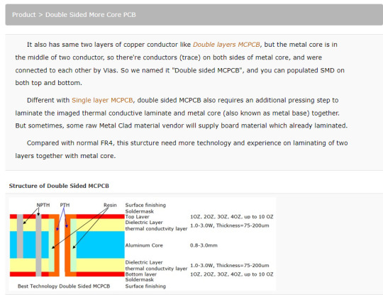
It also has same two layers of copper conductor like Double layers MCPCB, but the metal core is in the middle of two conductor, so there're conductors (trace) on both sides of metal core, and were connected to each other by Vias. So we named it "Double sided MCPCB", and you can populated SMD on both top and bottom.
Different with Single layer MCPCB, double sided MCPCB also requires an additional pressing step to laminate the imaged thermal conductive laminate and metal core (also known as metal base) together. But sometimes, some raw Metal Clad material vendor will supply board material which already laminated.
Compared with normal FR4, this sturcture need more technology and experience on laminating of two layers together with metal core.
0 notes
Text
Full Product Lines of Printed Circuits Boards
Based on different base material, there're three basic types but not limited to: FR-4/3/2 PCB, CEM-3 PCB, Metal Core PCB and Special PCB series (such as Ceramic PCB).
For FR-4 PCB, right now, we just class it into S/S PCB, 2 Layers PCB, Multi-Layers PCB (20 layers).
For MCPCB, which full name is Metal Core Printed Circuit Board, there're single layer MCPCB, double layers MCPCB and double sided MCPCB (2 layers on each side).
Special PCB, in fact, should be sorted to above two tapes, but considering special requirements, so we list it seperated. Right now, we can make RF boards (Rogers, Taconic materials), Heavy Copper PCB (4~20 OZ/ft2), Ceramic PCB, HDI, and so on.
0 notes
Text

COB MCPCB, known as "Chip-On-Board" Metal Core PCB, is a type of MCPCB used in thermoelectric separation application. By using COB MCPCB, the micro-chip (also known as "die") directly touch the metal core where the heat dissipate, and electrically interconnect the trace of circuit board (wire-bonding) so that power supply can be provided.In normal MCPCB, there's a dielectric layer between trace copper and metal core, and the thermal conductivity is limited by that dielectric layers, so value can only be 1~3 W/m.K. But using COB MCPCB, there's no such dielectric layer because chip (die) direct touch the metal core, so thermal conductivity value of COB MCPCB will be almost the same one of metal core material itself. The normal material of metal core is aluminum, so thermal conduviity of COB MCPCB is more than 200W/m.K.COB process consists of three main categories to perform when manufacturing the Chip-on-Board:1st: 'die mount or die attach';2nd: 'wire bonding';3rd: 'the encapsulation of die wires'.By using wire bonding & epoxy packaging then directly embedded on MCPCB, this practice can extend the lifespan of LED and unified light emission.According to process and material, COB MCPCB applications can be categorized into two types: Mirror Aluminum and silver or gold platting aluminum, or silver plating mirror aluminum PCB.
0 notes
Text
Bend radius is the minimum degree the flex area can bend. Use the chart below to calculate bend radius on your next design.
Knowing the life cycle bending times of your flex PCB is crucial to your design. If a flexible board is bent more times than the design allows for, the copper will begin to stretch and crack.
Semi-static: A flexible PCB that flexes a maximum of 20 times.
Dynamic: A flexible PCB that is regularly flexed and twisted.
Neutral Bend Radius
The neutral bend radius is the plane where there is no tension or compression when the circuit is flexed. Designing a balanced construction is the best way to center the neutral bend radius. Placing copper plane layers near the center of the material stack also keeps the neutral bend radius centered.
Please note that the use of images and links should comply with ethical and legal standards, and should provide value and a good user experience to the audience. It is also important to follow the rules and policies of the forum or website to avoid being banned or penalized.
1 note
·
View note