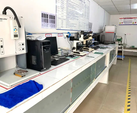
#BGA Assembly
Explore tagged Tumblr posts
Visit Tumblr Blog
Explore Tumblr blogs with no restrictions, modern design and the best experience.
Last Seen Tumblr Blogs


Fun Fact
Tumblr was acquired by Yahoo for $1.1B in 2013.
Text

BGA assembly is a process of mounting ball grid arrays onto a PCB using the solder reflow process. They are surface-mount components that use arrays of solder balls to make electrical interconnections. These solder balls melt and establish interconnection when the board passes through the solder reflow oven.
What are the advantages of a BGA assembly?
Improves both electrical and thermal performance while making efficient use of space.
Reduces the overall thickness of the board.
Minimizes the chances of PCB damage since BGA leads are made from solid solder balls, consequently reducing maintenance and repair times.
Suitable for miniature packages with high pin count.
Offers improved solderability, resulting in a speedy assembly procedure.
Dissipates heat quickly due to low thermal resistance.
As leading one-stop PCB Assembly services provider in China, Hitech Circuits offers high quality, cost effective and express PCB board products. If you have PCBA manufacturing needs, feeel free to contact us. For more information about PCB assembly, you can visit our website: https://hitechcircuits.com/pcb-assembly/
0 notes
Text
Ball Grid Array (BGA) technology has revolutionized PCB assembly by offering compact, high-performance, and thermally efficient packaging. With multiple types like PBGA, CBGA, FCBGA, and PoP, each designed for specific applications, BGA continues to be a key component in modern electronics, from smartphones to aerospace systems.
0 notes
Text
Exploring BGA Assembly: The Key to High-Performance Electronics
Ball Grid Array (BGA) assembly has become a critical technology in the manufacturing of modern electronic devices, offering superior performance and reliability compared to traditional packaging methods. As electronic devices continue to shrink in size while increasing in complexity, BGA has emerged as the go-to solution for mounting integrated circuits (ICs) on printed circuit boards (PCBs). This article delves into the principles of BGA assembly, its benefits, the process involved, and why it has become essential in high-performance electronics.

What is BGA Assembly?
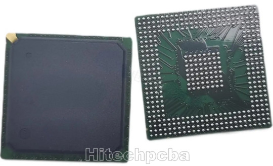
Ball Grid Array (BGA) is a type of surface-mount packaging used for mounting integrated circuits (ICs) onto PCBs. Unlike conventional packages that use leads or pins to make connections, BGA packages use a grid of small solder balls on the underside of the IC, which directly connect to corresponding pads on the PCB. The solder balls are typically made of a tin-lead or lead-free alloy and are arranged in a grid pattern. When the package is placed on the PCB and heated, the solder balls melt, creating a strong electrical and mechanical connection.
BGA assembly is favored for its ability to handle high-density packaging, improve thermal performance, and increase reliability. With the rapid growth of mobile devices, computers, and other high-performance electronics, BGA has become the preferred choice for many manufacturers.
The BGA Assembly Process
The BGA assembly process involves several crucial steps, from PCB preparation to final testing. Here’s an overview of the typical BGA assembly process:
1. PCB Preparation
Before the BGA component can be placed on the PCB, the board needs to be prepared. This step includes cleaning the board to remove any dirt or contaminants that could interfere with soldering. Next, a layer of solder paste is applied to the PCB pads that will correspond with the BGA’s solder balls. The solder paste is typically applied using a stencil to ensure precision.
2. Component Placement
In this step, the BGA component is aligned and placed onto the PCB. This is typically done using automated pick-and-place machines, which use precision robotics to pick up the BGA package and place it onto the PCB pads covered with solder paste. Unlike other surface-mount packages, the BGA package has no leads sticking out, making placement easier and more precise.
Due to the high number of solder balls in a typical BGA package, accurate placement is essential to avoid misalignment, which can lead to poor electrical connections and device failure.
3. Reflow Soldering
Once the BGA component is placed on the PCB, the assembly enters the reflow soldering phase. The entire PCB is heated in a reflow oven, where the temperature gradually rises until the solder paste melts, creating a strong bond between the BGA balls and the PCB pads. After the solder melts, it solidifies as the PCB cools, forming a reliable connection between the BGA and the board.
Reflow soldering is particularly advantageous in BGA assembly because it allows the solder balls to melt simultaneously, ensuring uniform solder joints around the entire package. This process eliminates the risk of cold or dry solder joints, which can result in electrical failures.
4. Inspection and Testing
After reflow soldering, the PCB undergoes inspection to ensure that the BGA has been properly soldered and that there are no defects in the connections. One of the key challenges in BGA assembly is ensuring the quality of solder joints, which are hidden under the package and not visible for visual inspection.
To address this, manufacturers use specialized inspection techniques:
X-Ray Inspection: X-ray imaging is commonly used to inspect the hidden solder joints beneath the BGA package. This allows for the detection of issues such as solder bridges, voids, or incomplete joints that could affect performance.
Automated Optical Inspection (AOI): While AOI is effective for inspecting surface-mounted components, it cannot directly inspect BGA solder joints. However, it is still useful for checking the placement of components and overall board quality.
Electrical Testing: Functional or in-circuit testing is conducted to verify that the BGA connections are electrically sound and the assembled PCB functions as expected.
5. Final Assembly and Packaging
Once the BGA component has passed inspection and testing, the PCB is integrated into its final assembly. This may involve attaching the PCB to other components, encasing it in a protective housing, or connecting it to a power supply or other systems. The finished product is then packaged for shipment or further distribution.
Advantages of BGA Assembly
BGA assembly offers several advantages, which explain why it is increasingly used in high-performance electronics manufacturing:
1. Higher Density and Compactness
One of the key benefits of BGA assembly is its ability to accommodate a high number of connections in a relatively small space. The grid of solder balls enables dense packaging, which allows more components to fit on the PCB without sacrificing size. This is crucial in devices like smartphones and laptops, where space is limited but performance needs are high.
2. Improved Electrical Performance
The BGA package’s direct connection between the chip and the PCB, using the solder balls as conductive paths, reduces the electrical resistance and improves signal integrity. This leads to faster, more reliable signal transmission, making BGA ideal for high-speed circuits and data-intensive applications.
3. Superior Thermal Performance
BGA packages also offer superior heat dissipation compared to traditional packages with leads or pins. The grid of solder balls allows for better heat distribution across the PCB, which is especially important for high-power or high-performance devices that generate a significant amount of heat.
4. Greater Reliability
BGA connections are more robust than traditional leaded packages because the solder balls provide multiple contact points, reducing the risk of mechanical failure. This is especially important in applications where durability and long-term reliability are critical, such as automotive, aerospace, and industrial devices.
5. Smaller Footprint
BGA assemblies have a much smaller footprint than other packaging types, such as leaded packages or chip-on-board (COB) configurations. The reduced size allows for more efficient use of PCB real estate and contributes to the overall compactness of modern devices.
Challenges of BGA Assembly
Despite its many benefits, BGA assembly does come with its own set of challenges:
Inspection and Testing: As mentioned, BGA solder joints are hidden under the component, making it difficult to visually inspect the connections. While X-ray inspection can address this issue, it is expensive and adds to the overall manufacturing cost.
Placement Accuracy: BGA components have a high number of solder balls, and precise placement is essential for creating reliable connections. Misalignment can result in poor performance or failure, which requires meticulous control during the assembly process.
Conclusion
BGA assembly plays a pivotal role in the development of high-performance, compact, and reliable electronic devices. By offering advantages in terms of density, electrical performance, thermal management, and reliability, BGA has become a staple in industries ranging from consumer electronics to automotive and medical technology. Despite challenges related to inspection and placement, advances in automation and inspection technologies continue to enhance the BGA assembly process, ensuring that it remains a cornerstone of modern electronics manufacturing. As technology continues to evolve, BGA assembly will likely remain a key enabler of the increasingly complex and compact devices that define our digital world.
0 notes
Text
Mastering the future, choose an outstanding partner for PCB and PCBA production!
🌐 Extensive Expertise: We are industry leaders in PCB and PCBA production, excelling in handling various complex circuit board requirements. Regardless of the scale of your project, we provide comprehensive solutions to ensure the perfect realization of your creative ideas.
🚀 Agile Response, Efficient Delivery: Time is the key to success. We take pride in our agility and efficiency, responding promptly to your needs and delivering high-quality products in the shortest possible time. Whether it’s an urgent project or a regular order, we deliver with swift precision.
🤝 Full Collaboration, Proactive After-Sales: We understand the true meaning of collaboration. We not only closely collaborate with you during the production phase to ensure smooth processes, but our after-sales service is also actively proactive. Any questions, requirements, or issues will be swiftly addressed with solutions.
Choosing us is choosing a guarantee of trust, quality, and efficiency. Partner with us to jointly create future technological wonders!
3 notes
·
View notes
Text
0 notes
Text
What is PCB Assembly ?
PCB Assembly manufacturer - Hitech Circuits Co., Limited
It’s the step in the manufacturing process in which you populate a blank board with the electronic components needed to make it into a functional printed circuit board. It’s these components that make a board into the circuit that enables an electronic product to function. PCB assembly typically takes place via one of two processes:
1. Surface-mount technology
SMT: SMT stands for “Surface Mount Technology“. The SMT components are very small sizes and comes in various packages like 0201, 0402, 0603, 1608 packages for resistors and capacitors. Similarly for Integrated circuits ICs we have SOIC, TSSOP, QFP and BGA.
The SMT components assembly is very difficult for human hands and can be time taking process so it is mostly done by automated pick and place machine.
2. Through-hole manufacturing
THT: THT stands for “Through hole Technology”. The components with leads and wires, like resistors, capacitors, inductors, PDIP ICs, transformers, transistors, IGBTs, MOSFETS are example.
The component has to be inserted on one side of PCB and pulled by leg on other side and cut the leg and solder it. The THT components assembly is usually done by hand soldering and is relatively easy.
Printed Circuit Board Assembly Techniques
There are only two common PCBA techniques available for use by a PCB designer. The methods are:
1. Automated PCB Assembly Techniques
Generally, this technique employs the use of state of the art machines, which are fully automatic. For example, the surface mount components are worth positioning with the aid of an automated pick and place machine.
Again, reflow soldering is commonly for surface mount components usually done in a reflow oven. An automated solder stencil is also used to apply the solder paste on the PCB.
Finally, high tech inspection machines are used to confirm and check the quality of the PCBA. Some of which include: Automated optical inspection machine (AOI), X-ray inspection machines, etc.
Above all, due to the precise monitoring, control of soldering, no human input and versatile machines.
This technique ensures utmost efficiency, output consistencies, and limits defects.
2. Manual PCB Assembly Techniques
This method is favorite for use with through-hole parts, which needs manual placement on the board. Besides, with these through-hole parts, it’s advisable you use wave soldering. Note that in the through- hole assembly process, you need to place the components and electronics on the PCB.
After that, you use wave soldering to solder the leads. Typically, you will need an individual to insert a component into a marked PTH. Once done, transfer the PCB to the next station where the next person will be on standby tasked with fixing another part.
What are the Benefits of SMT PCB Assembly?
SMT assembly provides many benefits and some of them are as follows:
It can be used to incorporate small components.
In SMT, the components can be placed on both sides of the board.
It assures high component densities.
Fewer holes need to be drilled for surface mounting than through-hole.
It require low initial costs and time for setting up the mass production.
SMT is the simpler and faster-automated assembly when compared to through-hole.
Errors regarding the component placement can be easily rectified.
Surface mount PCBs feature strong joints, which can easily withstand vibrations.
What are the techniques used in Surface Mount Technology?
There are several techniques for the reflow process. After applying the solder paste or a flux mixture on the board and after placing the components, the boards are conveyed to a reflow soldering oven. The techniques used for reflowing soldering include infrared lamps, hot gas convection, fluorocarbon liquids with a high boiling point, and so on.
What are the different testing methods used in SMT PCB Assembly?
Hitech Circuits as the PCB assembly manufacturer, we perform the following testing and inspection to ensure the quality of surface mount PCBs.
Automated Optical Inspection (AOI): This is performed before and after the soldering to identify the component placement, presence, and solder quality.
X-ray Testing: In this type of testing, the operator relies on the X-ray images of the PCB to check the solder joints and lead-less components such as Quad Flat Packs and ball grid arrays, which are generally not visible to naked eyes.
In-Circuit Testing (ICT): This method is used to detect manufacturing defects by testing the electrical properties in the SMT Assembly.
What type of files or documents should I send for SMT PCB Assembly?
Gerber Files: The file contains all details of physical board layers including solder masks, copper layers, drill data, legends, and so on.
Bill of Materials (BOM): This contains information on the list of items needed for the PCB manufacturing and the instructions of manufacturing.
Pick and Place File: This file contains information on all components to be used in the PCB design and their rotation and X-Y coordinates.
The whole process of PCB Assembly
1. Bare board loader machine
The first step in the PCB assembly is to arrange the bare boards on the rack, and the machine will automatically send the boards one by one into the SMT assembly line.
2. Printing solder paste
When PCB on the SMT production line, firstly, we have to print solder paste on it, and the solder paste will be printed on the pads of the PCB. These solder pastes will be melt and solder the electronic parts to the circuit board when it passes through the high-temperature reflow oven.
In addition, when testing new products, some people will use film board/adhesive cardboard instead of solder paste, which can increase the efficiency for adjusting the SMT machines.
3. Solder paste inspection machine(SPI)
Since the quality of solder paste printing is related to the quality of welding of subsequent parts, some SMT factories will use optical machine to check the quality of solder paste after printed the solder paste in order to ensure stable quality. If there any poorly printed solder paste board, we will wash off the solder paste on it and reprint, or remove the excess solder paste if there is redundant solder paste on it.
4. High speed SMT machine
Usually, we will put some small electronic parts (such as small resistors, capacitors, and inductors) to be printed on the circuit board first, and these parts will be slightly stuck by the solder paste just printed on the circuit board, so even if the speed of printing is very fast and the parts on the board will not fall away. But large parts are not suitable for use in such high speed SMT machines, which will slow down the speed of small parts assembly. And the parts will be shifted from the original position due to the rapid movement of the board.
5. Universal SMT machine
Universal SMT machine is also known as "slow machine", it will be assembled some large electronic components, such as BGA IC, connectors, etc., these parts need more accurate positions, so the alignment is very important. Use a camera to take a picture to confirm the position of the parts, so the speed is much slower than High speed SMT machine we taked before. Due to the size of the components here, not all of them are packed in tape and reel, and some may be packed in trays or tubes. But if you want the SMT machine to recognize the trays or tube-shaped packaging materials, you must configure an additional machine.
Generally, traditional SMT machines are using the principle of suction to move electronic parts, and in order to place the parts successfully, and there must be the flat surface on these electronic components for the suction nozzle of the SMT machine to absorb. However, for some electronic parts don’t have a flat surface for these machines, and it is necessary to order special nozzles for these special-shaped parts, or add a flat tape on the parts, or wear a flat cap for thees electronic parts.
6. Manual parts or visual inspection
After assembled all parts by the high speed SMT machine or Universal SMT machine and before going through the high-temperature reflow oven, and we will set up a visual inspection station here and to pick out the deviation parts or missing components boards etc., because we have to use a soldering iron to repair if there are still defectives boards after passing the high-temperature oven, which will affect the quality of the product and will also increase the cost. in addition, for some larger electronic parts or traditional DIP parts or some special reasons cannot be processed by the SMT machine before, they will be manually placed on pcb here.
7. Reflow oven
The purpose of reflow oven is to melt the solder paste and form a non-metallic compound on the component feet and the circuit board, that means to solder electronic components on the circuit board. The temperature rise and fall curves often affect the soldering quality of the entire circuit board. According to the characteristics of the solder materials, usually the reflow oven will set the preheating zone, soaking zone, reflow zone, and cooling zone to achieve the best soldering effect.
For example, the melting point for SAC305 solder paste with lead-free is about 217°C, which means that the temperature of the reflow oven must be higher than the melting points to remelt the solder paste. What's more, the maximum temperature in the reflow furnace should not exceed 250°C, otherwise many parts will be deformed or melted because they cannot withstand such a high temperature.
Basically, after the pcb passed through the reflow oven, the assembly for the entire circuit board is almost complete. If there are hand-soldered parts, we need to transfer to DIP process, and then we have to check the quality after reflow oven by QC department.
8. Automatic optical inspection(AOI)
The main purpose of setting up AOI is because some high density boards can’t be process the following ICT test, so we used AOI inspection to replace it. But even using AOI inspections, there still have the blind spots for such checking, for example, the solder pads under the components cannot be checked by AOI. At present, it can only check whether the parts have side standing issue, missing parts, displacement, polarity direction, solder bridges, lack of soldering etc., but cannot checking the BGA solderability, resistance value, capacitance value, inductance value and other components quality, so far AOI inspection can’t completely replace ICT test.
Therefore, there is still some risk if only AOI inspection is used to replace ICT testing, but ICT test is also not 100% make sure the good quality, we suggest these two ways can be combined with together to make sure the good quality.
9. PCB unloader machine
After the board is fully assembled, it will be retracted to the unloder machine, which has been designed to allow the SMT machine to automatically pick and place the board without damaging the quality for PCB.
10. Visual inspection for finished products
Normally there will be a visual inspection area in our SMT production line whether there is an AOI station or not, and it will help to check if there are any defectives after completed assembled the pcbs. If there is an AOI station, it can reduce the visual inspection worker on our SMT line, and to reduce the potential cost, and because it is still necessary to check some places that cannot be judged by AOI, many SMT factories will provide the mainly visual inspection templates at this station, which is convenient for visual inspection worker to inspect some key parts and polarity for components.
11. DIP process
DIP process is a very important process in the whole PCBA processing, and the processing quality will directly affect the functional for PCBA boards, so it is necessary to pay more attention to the DIP process. There are many preliminary preparations for DIP process. The basic process is to re-process the electronic components first, like to cut the extra pins for some DIP components, our staff received the components according to the BOM list, and will check whether the material part numbers and specifications are correct or not, and performs pre-production pre-processing according to the PCBA samples. The steps are: Use various related equipment (automatic capacitor pins cutting machine, jumper bending machine, diode and triode automatic forming machine, automatic belt forming machine and other machines) for processing.

12. ICT test
Printed Circuit board open/short circuit test (ICT, In-Circuit Test), The purpose of ICT test is mainly to test whether the components and circuits on the printed circuit board are open or short issues. It can also measure the basic characteristics of most components, such as resistance, capacitance, and inductance values to judge whether the functions of these parts are damaged, wrong parts or missing parts etc. after passing through the high-temperature reflow oven.
ICT test machines are divided into advanced and basic machines. The basic ICT test machines are generally called MDA (Manufacturing Defect Analyzer). It’s just to measure the basic characteristics of electronic components and judge open and short circuits issue we talked above.
In addition to all the functions of the basic ICT test machines, for advanced ICT test machine can also test the whole PCBA by using power, start to testing the PCBA boards by setting the program in the test machine. The advantage is that it can simulate the function of the printed circuit board under the actual power-on condition, this test can partly replace the following functional test machine (Function Test). But the cost for the test fixture of this advanced ICT test can probably buy a car, it’s too expensive and we suggest it can be used in mass production products.
13. PCBA function test
Functional testing is to make up for the ICT test, because ICT only tests the open and short circuits on the the PCBA board, and other functions such as BGA and other fuctions are not tested, so it is necessary to use a functional testing machine to test all functions on the whole PCBA board.
14. Cutting board (assembly board de-panel)
Normally, printed circuit boards will be produced in panel, and it will be assembled to increase the efficiency of SMT production. It means several single boards in one panel, such as two-in-one, four-in-one etc. After finished all the pcb assembly process, it needs to be cut into single boards, and for some printed circuit boards with only single boards also need to cut off some redundant board edges.
There are several ways to cut the printed circuit board. You can design the V-cut using the blade cutting machine (Scoring) or directly manually break off the board (not recommended). For more high density circuit boards, it will be used the professional splitting machine or the router to split the board without any damage the electronic components and printed circuit boards, but the cost and working hours will be a little longer.
Why Choose Hitech Circuits PCB Assembly Manufacturer for Your PCB Assembly Projects?
There are several PCB manufacturers specializing in PCB assemblyservices. However, Hitech Circuits PCB Assembly stands out owing to the following:
Assistance in Material Procurement:
Technically, in PCB assembly services, the quality of parts is the responsibility of the OEM; however, we ease your job by assisting you to make the right selection. We can help you procure all your parts of the same type own a single part number, thanks to our supply chain and vendor network as well as experience. This saves time and cost that goes in ordering single parts as you plan.
Testing procedures:
We are very focused on quality and thus implement stringent testing procedures at each stage of the assembly and after completion.
Fast Turnaround Times:
Our well-equipped facility and the right tools enable us to complete your requirements well before time, and without compromising on the quality or functioning of the PCBs. For simple designs we revert in 24 to 48 hours.
Cost Effectiveness:
While PCB assembly is a cost-effective alternative, we go a step further and assure that the parts you list are of a good quality and suitable for your requirement. Also, you can control the part flow and replenish them as needed. This eliminates the need to buy extra stock and store it.
Quick Quote:
We offer a quick quote based on your BOM. All you need is a detailed BOM, Gerber files, your application requirement sheet, and quantity.
We’re not one to stand still, which is why we use the latest equipment and the finest minds to create your PCB projects. We’re constantly keeping our finger on the pulse of the latest trends. And as a result, we know how to deliver the highest standards of PCB assembly to meet all your requirements.
Our dedicated, friendly customer service team also means that we support you every step of the way. Offering our expert guidance to ensure a complete PCB project that you’re happy with.
Contact us today
No matter what your printed circuit board assemblyneeds are, we always aim to deliver efficient, dependable solutions. For more information about our services, do not hesitate to get in touch with us today for a no-obligation quote
2 notes
·
View notes
Text
Boost SMT Quality with Automated Optical Inspection
Surface Mount Technology (SMT) has become the backbone of modern electronics manufacturing. As circuit boards grow more complex and component sizes continue to shrink, maintaining production quality has become more challenging. To address this, manufacturers rely on SMT automated optical inspection systems to enhance efficiency and ensure product reliability.
What Is SMT Automated Optical Inspection?
SMT automated optical inspection (AOI) is a high-speed visual inspection process used to verify the placement, alignment, and soldering of components on a printed circuit board (PCB). Using high-resolution cameras and advanced image processing algorithms, AOI systems scan each board for potential defects during or after assembly.
By catching issues early, these systems reduce rework, prevent defective units from moving forward, and increase yield rates. AOI is typically deployed at multiple points in the production line, including:
Post-solder paste inspection
Pre-reflow inspection
Post-reflow inspection
Each inspection stage targets specific issues such as insufficient solder, component misalignment, or solder bridging.
Why SMT AOI Is Critical to Electronics Manufacturing
The electronics industry demands tight tolerances and minimal defect rates. Even a single misplaced component can lead to product failure. Here's how SMT automated optical inspection supports manufacturing excellence:
1. Enhanced Accuracy
Automated inspection provides greater consistency than manual methods. It can detect:
Incorrect component orientation
Missing components
Cold solder joints
Tombstoning and lifted leads
These defects are often too subtle or time-consuming to spot with manual inspection.
2. Real-Time Feedback
Modern AOI systems integrate seamlessly into SMT lines, providing real-time defect detection and process feedback. When an issue is identified, operators receive alerts to make immediate adjustments. This minimizes downtime and material waste.
3. Scalable Performance
As demand increases, manual inspection becomes a bottleneck. AOI systems handle high-speed production environments with ease, inspecting hundreds of boards per hour without sacrificing accuracy. This makes SMT automated optical inspection ideal for both high-volume and high-mix production lines.
Benefits of Implementing AOI in SMT Production
Investing in AOI provides a range of tangible benefits:
Improved Product Quality: Early detection leads to fewer returns and better customer satisfaction.
Lower Operational Costs: Reducing scrap and rework translates to cost savings.
Faster Time to Market: Streamlined inspection accelerates the production cycle.
Compliance and Traceability: AOI systems often include data logging and defect classification features, aiding in quality audits and process optimization.
Common Defects Detected by SMT AOI
Effective inspection covers a wide array of potential issues, including:
Component misplacement
Solder bridges
Open circuits
Polarity errors
Solder balling
Insufficient or excessive solder
With high-resolution imaging and intelligent algorithms, AOI tools identify and classify these defects rapidly and with minimal human oversight.
Integrating AOI with Other SMT Equipment
For optimal results, AOI should be part of a fully integrated SMT inspection strategy. When combined with solder paste inspection (SPI) and X-ray inspection, manufacturers gain a full view of the assembly process. This layered approach ensures each stage is validated before moving to the next.
For instance, SPI evaluates solder paste deposition before components are placed, while AOI checks component placement and solder joints. In cases where defects may be hidden (like under BGAs), X-ray inspection complements AOI to provide a complete defect profile.
Choosing the Right AOI System
Selecting an appropriate AOI solution depends on several factors:
Board complexity
Component density
Production volume
Required inspection speed
Advanced AOI systems offer features such as 3D imaging, machine learning algorithms, and intuitive software interfaces. These innovations reduce false calls, simplify programming, and improve inspection reliability.
To explore AOI systems designed specifically for SMT applications, visit ASC International. Their cutting-edge technology supports manufacturers looking to improve inspection accuracy and throughput.
Final Thoughts
As electronics manufacturing grows more demanding, quality assurance tools must keep pace. SMT automated optical inspection provides the speed, accuracy, and consistency needed to meet today’s rigorous production standards. By identifying defects early and ensuring high-quality output, AOI protects your bottom line and strengthens customer confidence.
0 notes
Text
Reliability and Testing of Rigid-Flex PCBs: Ensuring Long-Term Performance
Rigid-Flex PCBs are widely used in high-reliability applications such as aerospace, medical devices, military electronics, and automotive systems. These boards are exposed to constant vibration, repeated bending, temperature fluctuations, and complex assembly conditions. Therefore, reliability testing is a critical step in the design and production process to ensure long-term functionality.
This article outlines key reliability factors and common test methods used for evaluating Rigid-Flex PCBs.
Why Rigid-Flex Reliability Is Challenging
Unlike traditional rigid boards, Rigid-Flex PCBs combine materials with different mechanical properties (e.g., FR-4 and polyimide) in a single laminated structure. This introduces challenges such as:
Mechanical stress concentration in bending zones
Mismatch in thermal expansion (CTE) between rigid and flexible areas
Potential delamination during reflow or operation
Higher risk of trace cracking in dynamic-flex zones
A failure in even a single flex section can lead to total product failure — especially in critical applications where repair is not possible (e.g., implantable medical devices or aerospace systems).
Key Reliability Factors
1. Dynamic Bending Fatigue
Rigid-Flex boards are often designed to bend repeatedly during use. Poor material selection or trace layout can cause copper cracking or delamination over time.
Solution: Use rolled-annealed copper, proper bend radius (≥10x thickness), and optimized trace routing.
2. Thermal Cycling and Shock
During operation or assembly, the PCB may experience sharp temperature changes (e.g., from -40°C to +125°C), causing expansion and contraction of different materials.
Solution: Choose materials with compatible CTE, and use high-Tg laminates.
3. Moisture Resistance
Exposure to humidity can lead to resin swelling, delamination, and corrosion over time.
Solution: Use polyimide-based flex cores and perform pre-bake before reflow to remove residual moisture.
Common Reliability Test Methods
1. Bending Cycle Test (Dynamic Flex Test)
Simulates repeated folding/unfolding of the flex section. Boards are bent thousands to millions of times at defined radii and speeds.
Evaluates copper fatigue and mechanical durability
Often required for wearable electronics or foldable devices
2. Thermal Cycling Test
PCBs are exposed to repeated temperature changes (e.g., -55°C to +125°C) for hundreds of cycles.
Detects micro-cracks, delamination, and solder joint failure
Used to verify performance under real-life temperature fluctuations
3. Peel Strength Test
Measures the bonding strength between copper and the dielectric substrate (usually in the flex area).
Helps identify weak adhesive systems or poor lamination quality
4. IPC 6013 & IPC-2223 Compliance
These are industry standards that define quality and reliability expectations for Rigid-Flex PCBs.
Class 2 (General electronic products)
Class 3 (High reliability, e.g. aerospace/medical)
5. Solderability Testing
Verifies that the surface finish (ENIG, OSP, etc.) maintains good solderability after storage or thermal aging.
6. Delamination Inspection (TMA, Cross-section, or X-ray)
Checks for layer separation, resin voids, or trapped air bubbles, especially at rigid-flex transition zones.
In-Process Testing and Quality Control
During manufacturing, the following checks help prevent defects early:
AOI (Automated Optical Inspection) for outer layer pattern
X-ray inspection for BGA pads or internal vias
Flying probe or electrical testing for continuity and shorts
Visual inspection of flex transition areas and coverlay alignment
Dimensional checks to confirm outline and cutout accuracy
Final Thoughts
Rigid-Flex PCBs deliver powerful benefits in compact, high-reliability applications — but only if designed and tested properly. From dynamic flexing to thermal endurance, these boards must survive complex real-world stresses over long periods.
By implementing comprehensive testing protocols and selecting materials and structures with proven reliability, manufacturers and engineers can ensure that their Rigid-Flex products meet the highest standards of performance and safety.

0 notes
Text
X-ray inspection of PCBA is a technology that uses the penetration of X-rays to perform non-destructive testing of the internal structure of circuit board assemblies. It mainly solves the problem of hidden solder joints and internal defects that cannot be observed by traditional optical means.
0 notes
Text
Precision PCBA Solutions by SFXPCB: Global Excellence in Electronics Manufacturing
In today’s fast-paced technological world, PCBA (Printed Circuit Board Assembly) is a fundamental process that powers every modern electronic device—from smartphones and medical instruments to aerospace equipment and industrial control systems. As electronic design becomes more complex, the need for a reliable and precise PCBA partner becomes even more crucial.
At the forefront of innovation and quality in PCBA manufacturing stands SFXPCB, a global provider trusted by industries in Germany, USA, UK, Austria, and Canada. SFXPCB delivers high-quality assembly, superior engineering support, and efficient global logistics—all while maintaining competitive pricing.
What is PCBA?

PCBA (Printed Circuit Board Assembly) refers to the process of assembling electronic components onto a bare PCB (Printed Circuit Board). This process involves:
Applying solder paste to board pads
Placing surface mount or through-hole components
Reflow or wave soldering
Inspection (AOI, X-ray, or visual)
Functional and quality testing
The final product is a fully functional electronic board, ready for integration into a finished device.
SFXPCB – Your Trusted PCBA Manufacturing Partner
With a strong manufacturing base in China and a broad international customer base, SFXPCB provides end-to-end PCBA services tailored to meet the highest industry standards. From prototype assembly to mass production, their process is defined by precision, consistency, and speed.
Why choose SFXPCB for your PCBA needs?
✅ 1. One-Stop PCBA Services
SFXPCB provides a complete PCBA solution, including:
PCB fabrication
Component sourcing (including hard-to-find parts)
SMT & THT assembly
Functional and in-circuit testing
Quality assurance and packaging
This streamlined approach minimizes delays and errors, ensuring your projects run smoothly from start to finish.
✅ 2. Advanced Technology & Capabilities
Equipped with state-of-the-art SMT lines, reflow ovens, AOI systems, and BGA placement equipment, SFXPCB can handle:
Fine-pitch ICs
BGA, QFN, CSP components
High-density interconnects (HDI)
Rigid, Flex, and Rigid-Flex PCBs
Their advanced capabilities make them a top choice for industries demanding high precision and miniaturization.
✅ 3. Unmatched Quality Control
SFXPCB strictly adheres to ISO9001, RoHS, and UL certifications. Each project undergoes:
Automated Optical Inspection (AOI)
X-ray inspection (for BGA and hidden joints)
Manual inspection by experienced technicians
Functionality testing based on customer requirements
You can trust that every assembly meets the highest standards.
Industries That Trust SFXPCB’s PCBA Services
SFXPCB’s ability to handle complex projects and deliver on time has made it the preferred PCBA manufacturer for companies in:
🚗 Automotive Electronics
Reliable and rugged PCBA for engine control units, infotainment, and safety systems.
🏥 Medical Devices
Precision PCBA used in imaging systems, diagnostics, monitoring devices, and wearables.
📡 Telecommunications
High-frequency, high-speed PCBs used in routers, base stations, and IoT gateways.
⚙️ Industrial Automation
Durable assemblies for sensors, controllers, and factory automation systems.
🛰 Aerospace & Defense
High-reliability PCBA for communication, navigation, and surveillance applications.
Global Reach, Local Focus
Though headquartered in China, SFXPCB is a global player, serving clients in:
Germany
United States
United Kingdom
Austria
Canada
Their responsive English-speaking support team and efficient international shipping make it easy to work with them, no matter where you're located.
Fast Turnaround and Competitive Pricing
SFXPCB understands that time-to-market is critical. That’s why they offer:
Rapid prototyping services
Flexible volume production (from 1 to 10,000+ units)
Competitive pricing without sacrificing quality
Through strong relationships with component suppliers and efficient manufacturing practices, SFXPCB delivers high-value PCBA services at a cost-effective rate.
How to Start Your PCBA Project with SFXPCB
Getting started with SFXPCB is simple and fast:
Visit the website: https://sfxpcb.com/
Upload your Gerber files and BOM
Get a fast and accurate quote
Review DFM suggestions from their engineers
Approve and track your order online
You’ll benefit from responsive communication, transparency, and a seamless production process from quote to delivery.
Customer Testimonials
“SFXPCB is our go-to partner for PCBA. They consistently deliver high-quality boards and help us hit tight deadlines.” — CTO, IoT Startup (Germany)
“The team at SFXPCB is incredibly responsive and knowledgeable. We’ve trusted them with multiple projects and never been disappointed.” — Procurement Manager, Medical Device Company (USA)
Contact SFXPCB Today
Have a question or ready to place an order? Reach out directly:
📧 Email: [email protected] 📞 Phone: +86 0755 21012004
In the world of modern electronics, the importance of a reliable PCBA provider cannot be overstated. From prototyping to full-scale production, SFXPCB combines precision, speed, and service excellence to help businesses across the globe bring their products to life.
Whether you're an electronics startup or a global OEM, SFXPCB delivers quality you can trust—on time and on budget.
0 notes
Text
What is the SMT Process for PCB Board Assembly?
The SMT PCB Board assembly process, or Surface Mount Technology process, is a strategy utilized to mount electronic components straightforwardly onto the surface of a printed circuit board (PCB). This advanced method has generally supplanted the more seasoned through-hole strategy due to its productivity, cost-effectiveness, and capacity to oblige miniaturized components. SMT permits for higher circuit densities and littler gadget profiles, making it the standard in today's hardware fabricating industry.
The SMT prepare includes a few basic steps, each planned to guarantee precision, unwavering quality, and execution of the last PCB assembly. These steps are regularly executed in a exceedingly mechanized environment to keep up accuracy and consistency.
1. Solder Paste Application
The to begin with step in the SMT PCB board assembly prepare is the application of solder paste. Solder paste is a blend of minor patch particles and flux. It is connected to the cushions on the PCB where components will be set utilizing a stencil and squeegee. This step is significant since the quality of solder paste application specifically influences the unwavering quality of patch joints.
2. Pick and Place
After the solder paste is connected, the PCB moves to the pick-and-place machine. This computerized framework precisely picks surface mount devices (SMDs) from component reels or plate and places them onto the solder-pasted cushions on the PCB. The speed and accuracy of this machine permit for quick assembly of thickly pressed circuit boards.
3. Reflow Soldering
Once all components are set on the SMT PCB Board, the assembly enters a reflow broiler. The broiler slowly warms the board through a controlled temperature profile. The solder paste dissolves (reflows) and shapes a solid electrical and mechanical bond between the components and the PCB cushions. The board is at that point cooled, setting the connections.

4. Inspection and Quality Control
Post-reflow, the assembly experiences assessment to confirm the quality of the patch joints and adjust component situation. This step frequently incorporates Automated Optical Inspection (AOI), which employments cameras to identify issues such as misalignment, lost components, or patch bridges. For complex assemblies, X-ray assessment may moreover be utilized, particularly to look at covered up patch joints beneath components like BGAs (Ball Grid Arrays).
5. Rework and Repair (on the off chance that needed)
If any surrenders are found amid review, the SMT PCB board may be sent for adjust. Talented specialists utilize revamp stations to expel, supplant, or resolder components as essential. Progressed devices guarantee that revamp does not harm the board or encompassing components.
6. Functional Testing
Finally, the board may go through utilitarian testing, where it is powered up and tried in conditions comparative to real-world utilize. This guarantees the PCB performs as expecting some time recently it moves on to last item assembly or shipping.
In conclusion, the SMT prepare for PCB board assembly is a profoundly exact and effective strategy that empowers the generation of compact, high-performance electronic devices. From solder paste printing to reflow fastening and testing, each organize plays a crucial part in the creation of dependable and strong SMT PCB sheets that control today’s progressed advances.
0 notes
Text

Reliable BGA PCB Assembly Services – High Precision & Quality
Looking for expert BGA PCB assembly? We offer precise Ball Grid Array (BGA) assembly with advanced inspection and rework capabilities. Ideal for high-density and compact PCB designs. Trusted by industries for reliable performance and quality. Get a quote today!
0 notes
Text
Exploring BGA Assembly: The Key to High-Performance Electronics
Ball Grid Array (BGA) assembly has become a critical technology in the manufacturing of modern electronic devices, offering superior performance and reliability compared to traditional packaging methods. As electronic devices continue to shrink in size while increasing in complexity, BGA has emerged as the go-to solution for mounting integrated circuits (ICs) on printed circuit boards (PCBs). This article delves into the principles of BGA assembly, its benefits, the process involved, and why it has become essential in high-performance electronics.

What is BGA Assembly?
Ball Grid Array (BGA) is a type of surface-mount packaging used for mounting integrated circuits (ICs) onto PCBs. Unlike conventional packages that use leads or pins to make connections, BGA packages use a grid of small solder balls on the underside of the IC, which directly connect to corresponding pads on the PCB. The solder balls are typically made of a tin-lead or lead-free alloy and are arranged in a grid pattern. When the package is placed on the PCB and heated, the solder balls melt, creating a strong electrical and mechanical connection.
BGA assembly is favored for its ability to handle high-density packaging, improve thermal performance, and increase reliability. With the rapid growth of mobile devices, computers, and other high-performance electronics, BGA has become the preferred choice for many manufacturers.
The BGA Assembly Process
The BGA assembly process involves several crucial steps, from PCB preparation to final testing. Here’s an overview of the typical BGA assembly process:
1. PCB Preparation
Before the BGA component can be placed on the PCB, the board needs to be prepared. This step includes cleaning the board to remove any dirt or contaminants that could interfere with soldering. Next, a layer of solder paste is applied to the PCB pads that will correspond with the BGA’s solder balls. The solder paste is typically applied using a stencil to ensure precision.
2. Component Placement
In this step, the BGA component is aligned and placed onto the PCB. This is typically done using automated pick-and-place machines, which use precision robotics to pick up the BGA package and place it onto the PCB pads covered with solder paste. Unlike other surface-mount packages, the BGA package has no leads sticking out, making placement easier and more precise.
Due to the high number of solder balls in a typical BGA package, accurate placement is essential to avoid misalignment, which can lead to poor electrical connections and device failure.
3. Reflow Soldering
Once the BGA component is placed on the PCB, the assembly enters the reflow soldering phase. The entire PCB is heated in a reflow oven, where the temperature gradually rises until the solder paste melts, creating a strong bond between the BGA balls and the PCB pads. After the solder melts, it solidifies as the PCB cools, forming a reliable connection between the BGA and the board.
Reflow soldering is particularly advantageous in BGA assembly because it allows the solder balls to melt simultaneously, ensuring uniform solder joints around the entire package. This process eliminates the risk of cold or dry solder joints, which can result in electrical failures.
4. Inspection and Testing
After reflow soldering, the PCB undergoes inspection to ensure that the BGA has been properly soldered and that there are no defects in the connections. One of the key challenges in BGA assembly is ensuring the quality of solder joints, which are hidden under the package and not visible for visual inspection.
To address this, manufacturers use specialized inspection techniques:
X-Ray Inspection: X-ray imaging is commonly used to inspect the hidden solder joints beneath the BGA package. This allows for the detection of issues such as solder bridges, voids, or incomplete joints that could affect performance.
Automated Optical Inspection (AOI): While AOI is effective for inspecting surface-mounted components, it cannot directly inspect BGA solder joints. However, it is still useful for checking the placement of components and overall board quality.
Electrical Testing: Functional or in-circuit testing is conducted to verify that the BGA connections are electrically sound and the assembled PCB functions as expected.
5. Final Assembly and Packaging
Once the BGA component has passed inspection and testing, the PCB is integrated into its final assembly. This may involve attaching the PCB to other components, encasing it in a protective housing, or connecting it to a power supply or other systems. The finished product is then packaged for shipment or further distribution.
Advantages of BGA Assembly
BGA assembly offers several advantages, which explain why it is increasingly used in high-performance electronics manufacturing:
1. Higher Density and Compactness
One of the key benefits of BGA assembly is its ability to accommodate a high number of connections in a relatively small space. The grid of solder balls enables dense packaging, which allows more components to fit on the PCB without sacrificing size. This is crucial in devices like smartphones and laptops, where space is limited but performance needs are high.
2. Improved Electrical Performance
The BGA package’s direct connection between the chip and the PCB, using the solder balls as conductive paths, reduces the electrical resistance and improves signal integrity. This leads to faster, more reliable signal transmission, making BGA ideal for high-speed circuits and data-intensive applications.
3. Superior Thermal Performance
BGA packages also offer superior heat dissipation compared to traditional packages with leads or pins. The grid of solder balls allows for better heat distribution across the PCB, which is especially important for high-power or high-performance devices that generate a significant amount of heat.
4. Greater Reliability
BGA connections are more robust than traditional leaded packages because the solder balls provide multiple contact points, reducing the risk of mechanical failure. This is especially important in applications where durability and long-term reliability are critical, such as automotive, aerospace, and industrial devices.
5. Smaller Footprint
BGA assemblies have a much smaller footprint than other packaging types, such as leaded packages or chip-on-board (COB) configurations. The reduced size allows for more efficient use of PCB real estate and contributes to the overall compactness of modern devices.
Challenges of BGA Assembly
Despite its many benefits, BGA assembly does come with its own set of challenges:
Inspection and Testing: As mentioned, BGA solder joints are hidden under the component, making it difficult to visually inspect the connections. While X-ray inspection can address this issue, it is expensive and adds to the overall manufacturing cost.
Placement Accuracy: BGA components have a high number of solder balls, and precise placement is essential for creating reliable connections. Misalignment can result in poor performance or failure, which requires meticulous control during the assembly process.
Conclusion
BGA assembly plays a pivotal role in the development of high-performance, compact, and reliable electronic devices. By offering advantages in terms of density, electrical performance, thermal management, and reliability, BGA has become a staple in industries ranging from consumer electronics to automotive and medical technology. Despite challenges related to inspection and placement, advances in automation and inspection technologies continue to enhance the BGA assembly process, ensuring that it remains a cornerstone of modern electronics manufacturing. As technology continues to evolve, BGA assembly will likely remain a key enabler of the increasingly complex and compact devices that define our digital world.
1 note
·
View note
Text
BGA PCB Assembly
What’s BGA PCB?
BGA PCB is Printed Circuit Boards with Ball Grid Array. We use various sophisticated techniques for making BGA PCBs. Such PCBs have a small size, low cost, and high packaging density. Hence, they are reliable for high-performance applications.

What’s BGA PCB Assembly?
Ball Grid Array (BGA) assembly technology is a surface mount packaging technology applied to integrated circuits, which is often used to permanently fix devices such as microprocessors. BGA assembly can accommodate more pins than other packages such as Dual in-line packages or Quad Flat Packages, and the entire bottom surface of the device can be used as pins , instead of only peripherals available, and also have a shorter average wire length than peripheral-limited package types for better high-speed performance.
Our BGA assembly services cover a wide range, including BGA prototype development, BGA PCB assembly, BGA component removal, BGA replacement, BGA rework and reballing, BGA PCB assembly inspection, and so on. Leveraging our full-coverage services, we can help customers streamline the supply network and accelerate product development time.
Benefits of BGA PCB Assembly
Efficient Use of Space – BGA PCB layout allows us to efficiently use the available space, so we can mount more components and manufacture lighter devices.
Better Thermal Performance – For BGA, the heat generated by the components is transferred directly through the ball. In addition, the large contact area improves heat dissipation, which prevents overheating of components and ensures long life.
Higher Electrical Conductivity – The path between the die and the circuit board is short, which results in better electrical conductivity. Moreover, there is no through-hole on the board, the whole circuit board is covered with solder balls and other components, so vacant spaces are reduced.
Easy to Assemble And Manage – Compared to other PCB assembly techniques, BGA is easier to assemble and manage as the solder balls are used directly to solder the package to the board.
Less Damage to Leads – We use solid solder balls for manufacturing BGA leads. Hence, there is a lesser risk that they will get damaged during the operation.
In a word, BGA PCB assembly, have these advantages, high density, better electrical conductivity, lower thermal resistance, easy to assembly & manage are some of the advantages of BGA PCB.
Stringent BGA PCB Assembly Testing Process
To achieve the highest quality standards for BGA assembly, we use a variety of inspection methods throughout the process including optical inspection, mechanical inspection, and X-ray inspection. Among them, the inspection of BGA solder joints must use X-rays. X-rays can pass through the components to inspect the solder joints below them, so as to check the solder joint position, solder joint radius, and solder joint thickness.
Inspection of BGA PCB
We mostly use X-ray inspection for analyzing the features of BGA PCBs. This technique is known as XRD in the industry and relies on X-rays for unveiling the hidden features of this PCB. This kind of inspection reveals.
* Solder Joint Position
* Solder Joint Radius
* Change in Circular shape
* Solder Joint Thickness

The Hitechpcba advantage lies in a whole range of aspects, beginning from the fact that we have the proven technology available at our disposal. With over 15 years of experience in a wide range of PCB Fabrication and Assembly techniques, what we also have is trained manpower and importantly, robust industry experience and best practices that you can benefit from.
Our unstinting devotion to quality and customer satisfaction means that once you partner with us, you can rest assured that you will get nothing but the best. The customer-oriented approach also shows up in your commitment to delivery times. With quick turnaround times, you can reap the benefit of quick time-to-market, which, in turn, can be a major source of competitive advantage.
Whether your requirement is BGA PCB design, BGA PCB, BGA PCB layout, BGA PCB Assembly or BGA rework, you can rest assured that you will get superior quality and performance, that will in turn, positively impact the performance of your final product.
With our efficient network of component suppliers and the many economies of scale that we enjoy, that you will get optimal costs, is a given.
Please feel free to contact us ([email protected]) if you have any other special request on the BGA pcb assembly.
3 notes
·
View notes
Text
The Essential Guide to SMT Equipment in Modern Electronics Manufacturing

Introduction to SMT Equipment
SMT equipment (Surface Mount Technology equipment) is the backbone of modern electronics manufacturing. As consumer and industrial electronics continue to shrink in size while increasing in complexity, the demand for efficient and precise SMT machinery has grown exponentially. This guide explores the different types of SMT equipment, their functions, and their importance in producing high-quality printed circuit boards (PCBs).
Key Components of SMT Equipment
1. Solder Paste Printing Machines
The first step in the SMT assembly process is applying solder paste to the PCB. Solder paste printers use stencils to deposit precise amounts of solder paste onto the board’s pads. Advanced models feature:
Vision alignment systems for high accuracy
Automatic stencil cleaning to prevent clogging
Real-time inspection to detect printing defects
2. Pick-and-Place Machines
Pick-and-place machines are the most critical SMT equipment in the production line. They accurately place surface-mount components (SMDs) onto the PCB at high speeds. Modern pick-and-place machines offer:
High-speed placement (up to 100,000 components per hour)
Multi-nozzle systems for handling different component sizes
Machine vision systems for precision alignment
3. Reflow Ovens
After component placement, the PCB moves through a reflow oven, where the solder paste melts and forms strong electrical connections. Key features include:
Multiple heating zones for controlled temperature profiles
Nitrogen gas environments to reduce oxidation
Cooling systems to solidify solder joints quickly
4. Inspection and Testing Equipment
Quality control is crucial in SMT manufacturing, and inspection systems ensure defect-free production. Common SMT inspection tools include:
Automated Optical Inspection (AOI) – Detects misaligned or missing components
X-ray Inspection (AXI) – Examines hidden solder joints (e.g., under BGA components)
In-Circuit Testing (ICT) – Verifies electrical functionality
Advancements in SMT Equipment Technology
1. Automation and Industry 4.0 Integration
Modern SMT machines increasingly incorporate IoT (Internet of Things) and AI-driven analytics. Smart factories use real-time data to:
Optimize machine performance
Predict maintenance needs
Reduce downtime
2. Miniaturization and High-Density Assembly
As components shrink (e.g., 01005 resistors, ultra-fine-pitch ICs), SMT equipment must adapt with:
Higher placement accuracy (micrometer-level precision)
Advanced feeders for tiny components
Laser-assisted alignment for micro-BGA and QFN packages
3. Eco-Friendly SMT Solutions
Sustainability is becoming a priority in electronics manufacturing. New SMT machinery developments include:
Lead-free solder paste compatibility
Energy-efficient reflow ovens
Reduced chemical usage in cleaning processes
Choosing the Right SMT Equipment for Your Production Line
Selecting the best SMT machines depends on several factors:
1. Production Volume
Low to medium volume: Semi-automatic or benchtop SMT equipment
High volume: Fully automated high-speed pick-and-place and conveyor-based systems
2. Component Complexity
Standard SMDs: Basic pick-and-place machines
Advanced packages (e.g., PoP, SiP): Machines with 3D vision and multi-stage placement
3. Budget and ROI Considerations
Entry-level machines for startups
Mid-range systems for growing manufacturers
High-end solutions for large-scale production
Future Trends in SMT Equipment
The SMT industry continues to evolve with emerging technologies:
1. AI-Driven Process Optimization
Machine learning algorithms analyze production data to improve yield and reduce errors.
2. Hybrid SMT-THR Systems
Combining Surface Mount Technology (SMT) and Through-Hole Technology (THT) in a single line for flexible manufacturing.
3. 3D Printed Electronics Integration
Future SMT machines may incorporate additive manufacturing for customized PCB designs.
Conclusion
SMT equipment is essential for producing reliable and compact electronic devices. From solder paste printers to high-speed pick-and-place machines and inspection systems, each component plays a vital role in ensuring efficiency and quality. As technology advances, SMT machinery will continue to push the boundaries of precision, speed, and sustainability in electronics manufacturing.
By understanding the different types of SMT equipment and their applications, manufacturers can optimize their production lines for better performance and competitiveness in the fast-evolving electronics industry.
1 note
·
View note
Text
Aimtron: Your Reliable Partner for PCB Assembly Manufacturing Services in Illinois

In the fast-paced world of electronics manufacturing, having a trusted partner for PCB assembly services can make all the difference. That’s where Aimtron Corporation stands out. Located in the heart of Illinois, Aimtron has established itself as a leader in providing end-to-end PCB assembly and electronics manufacturing services to clients across a wide range of industries—from aerospace and defense to healthcare, industrial automation, and consumer electronics.
Why Choose Aimtron?
1. Comprehensive PCB Assembly Services
Aimtron offers a full spectrum of PCB assembly services including:
Surface Mount Technology (SMT)
Through-Hole Assembly
Turnkey PCB Assembly
BGA and Micro-BGA Assembly
Prototyping to Full-Scale Production
Whether you need a quick-turn prototype or high-volume production, Aimtron has the technology and expertise to deliver consistent quality.
2. State-of-the-Art Manufacturing Facility
At Aimtron’s Illinois facility, quality is more than a promise—it’s a standard. Equipped with cutting-edge SMT lines, automated optical inspection (AOI), X-ray inspection for BGAs, and in-circuit testing, Aimtron ensures every board meets the highest quality benchmarks.
3. Engineering Excellence
Aimtron doesn’t just assemble PCBs; it partners with clients from concept to production. Their team of skilled engineers provides:
Design for Manufacturability (DFM)
Design for Testability (DFT)
Component sourcing and BOM optimization
Technical support and value engineering
This collaborative approach reduces lead times, lowers costs, and enhances product reliability.
4. Commitment to Quality and Compliance
Aimtron is ISO 9001 and ISO 13485 certified, ITAR registered, and RoHS compliant, ensuring adherence to global quality and regulatory standards. Their robust quality management system supports continuous improvement and customer satisfaction.
5. Customer-Centric Approach
Aimtron believes in building long-term partnerships. Their customer-first philosophy translates into responsive communication, transparent pricing, and a flexible manufacturing model that adapts to changing project needs.
Serving Illinois and Beyond
While Aimtron proudly operates from Illinois, its reputation for reliability and precision extends far beyond state lines. Clients across the U.S. and internationally trust Aimtron for mission-critical electronics manufacturing solutions delivered on time and within budget.
Industries Served
Medical Devices
Aerospace & Defense
Automotive
Industrial Control
Consumer Electronics
IoT & Smart Devices
Let’s Build the Future Together
At Aimtron, innovation meets execution. With a perfect blend of technology, talent, and tenacity, Aimtron is not just a PCB assembly vendor—it’s your strategic partner in bringing great ideas to life.
Looking for a dependable PCB assembly manufacturer in Illinois? Partner with Aimtron and experience quality, reliability, and excellence every step of the way.
#ElectronicsManufacturing#PCBAssemblyServices#DesignforTestability#DesignforManufacturability#PCBassemblymanufacturerinIllinois#SurfaceMountTechnology#Through-HoleAssembly
0 notes