#PCBAssemblyServices
Text
Designing Tomorrow: Aimtron’s Impactful PCB Assembly Solutions
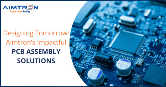
In the ever-evolving landscape of technology, Printed Circuit Boards (PCBs) play a pivotal role. These intricate electronic platforms serve as the backbone for countless devices, from smartphones to medical equipment. Among the trailblazers in this field is Aimtron, a company that doesn’t just design PCBs; it engineers solutions that shape the future.
Aimtron’s Vision and Expertise
Driven by a passion for progress and societal advancement, Aimtron excels in sourcing, building, and launching innovative products that enrich society globally. Their expertise in Electronic Design and Manufacturing Services sets them apart. Let’s delve into their impactful PCB assembly solutions:
1. PCB Assembly Services
At Aimtron, the journey from concept to production is seamless. Their dedicated team handles all your PCB needs, ensuring top-quality performance and reliability. Here are the types of PCBs Aimtron works with:
a. Flex PCBs (Flexible PCBs)
For applications requiring flexibility and durability, Aimtron’s flex PCBs are the ideal choice. Designed to bend and flex during use, these PCBs fit into tight or unusual spaces, providing reliable performance in dynamic environments.
b. Rigid-Flex PCBs
Combining the stability of rigid PCBs with the flexibility of flex circuits, Aimtron’s rigid-flex PCBs offer versatile solutions for complex electronic applications. These hybrid PCBs ensure reliability and performance, even in the most challenging environments.
c. Single-Sided PCBs
Ideal for simple electronic applications, Aimtron’s single-sided PCBs provide a cost-effective and reliable foundation for your components. They work well for low-density designs, ensuring quality and durability.
d. Double-Sided PCBs
With conductive layers on both sides, Aimtron’s double-sided PCBs offer more flexibility for complex circuits. These PCBs accommodate a higher component density, meeting the needs of sophisticated electronics.
e. Multilayer PCBs
For advanced electronic challenges, Aimtron’s multilayer PCBs provide the solution. Featuring three or more layers of conductive material, these PCBs are perfect for high-speed and high-frequency applications. They ensure signal integrity and reduce electromagnetic interference (EMI).
f. Rigid PCBs
Aimtron’s rigid PCBs offer a solid foundation for most electronics. Available in single-sided, double-sided, and multilayer configurations, they provide a stable and durable platform for a wide range of applications.
2. Chip-on-Board (COB) Technology
Aimtron employs COB technology, allowing direct attachment of bare semiconductor dies to the PCB. This results in smaller and more cost-effective solutions. The integration of COB technology enhances performance and reliability.
3. Design for Excellence (DfE)
Aimtron’s DfE method ensures efficient integration of components like PCBAs, wire harnesses, and mechanical enclosures. Collaborative engineering strategies streamline manufacturing, resulting in superior end products.
Conclusion
As we design tomorrow’s innovations, Aimtron’s impactful PCB assembly solutions pave the way. From flex PCBs to advanced multilayer designs, Aimtron’s commitment to excellence drives progress in the electronics industry. So, when you think of shaping the future, think Aimtron.
For more information, visit Aimtron’s website: Aimtron
#electronicsdesign#electronicsmanufacturer#pcbassembly#pcbassemblysolution#multilayerpcb#pcbdesign#pcbassemblyservices
0 notes
Text
DESIGNING THE FUTURE: AIMTRON’S VISION FOR PCB ASSEMBLY AND ELECTRONICS MANUFACTURING

Introduction:
In the rapidly evolving landscape of electronics manufacturing, the demand for innovative solutions and cutting-edge technology is more significant than ever. Aimtron, a frontrunner in PCB assembly and electronics manufacturing, is pioneering a vision that not only meets current industry needs but also shapes the future of electronic design and production. This blog explores Aimtron’s forward-thinking approach, highlighting the key aspects of their vision that set them apart in the dynamic world of electronics manufacturing.
Advanced PCB Assembly Technologies:
Aimtron places a strong emphasis on leveraging advanced technologies in PCB assembly. From automated pick-and-place machines to state-of-the-art soldering techniques, Aimtron ensures precision and efficiency in every step of the assembly process. By embracing the latest advancements in robotics, machine learning, and artificial intelligence, Aimtron optimizes production workflows, reduces errors, and enhances the overall quality of electronic components.
Customized Solutions for Diverse Industries:
One of Aimtron’s standout features is its commitment to providing customized solutions tailored to the unique requirements of various industries. Whether it’s automotive, aerospace, medical devices, or consumer electronics, Aimtron understands that each sector has distinct needs. By closely collaborating with clients, Aimtron develops bespoke manufacturing solutions that not only meet current demands but also anticipate future challenges in specific industries.
Environmental Sustainability:
In an era where environmental consciousness is paramount, Aimtron is at the forefront of sustainable electronics manufacturing. The company actively invests in eco-friendly practices, such as lead-free soldering, recycling programs, and energy-efficient manufacturing processes. Aimtron’s commitment to sustainability aligns with the global push towards greener technology, ensuring that their products not only meet performance standards but also contribute to a more sustainable future.
Real-time Data Analytics and Monitoring:
Aimtron understands the importance of real-time data analytics in ensuring the efficiency and quality of the manufacturing process. Through the integration of IoT (Internet of Things) devices and smart sensors, Aimtron monitors various parameters during production. This data-driven approach allows for proactive identification and resolution of issues, minimizing downtime and maximizing yield. Aimtron’s emphasis on data analytics positions them at the forefront of Industry 4.0, where connectivity and intelligent decision-making drive manufacturing excellence.
Agile and Adaptive Manufacturing:
The electronics industry is known for its rapid changes and evolving standards. Aimtron’s vision includes an agile and adaptive manufacturing approach, enabling quick responses to market demands and technological advancements. This flexibility ensures that Aimtron’s clients stay ahead in the competitive landscape, as they can swiftly incorporate design changes, scale production, and adapt to emerging trends without compromising on quality or efficiency.
Conclusion:
Aimtron’s vision for PCB assembly and electronics manufacturing is a testament to the company’s commitment to innovation, sustainability, and customer satisfaction. By combining cutting-edge technologies with a customer-centric approach, Aimtron is not only meeting the current needs of the industry but is actively shaping the future. As electronics continue to play a pivotal role in our daily lives, companies like Aimtron are leading the way in designing a future where precision, efficiency, and sustainability converge to create a new standard in electronics manufacturing.
#electronicsmanufacturing#electronicsmanufacturingservice#PCBAssembly#PCBAssemblyservice#PCBAssemblyservices
0 notes
Text
Find expert tips on selecting the perfect PCB manufacturer for your project. Learn about key factors, cost considerations, and quality assurance to ensure a successful partnership.
#PrintedCircuitBoard#PCBManufacturers#CircuitBoardManufacturing#PCBAssembly#ElectronicManufacturing#PCBPrototyping#PCBDesign#PCBProduction#PCBIndustry#PCBSolutions#PCBManufacturer#PrintedCircuitBoardAssembly#PCBManufacturingProcess#PCBQuality#PCBTechnology#PCBComponents#PCBAssemblyServices#PCBExporters#PCBInnovation#PCBTesting#PCBExperts#PCBManufacturingCompany
1 note
·
View note
Text
Know About Etching Techniques in PCB Assembly Process
The complexity of circuit boards has increased in terms of design and circuitry. For the circuit board to function normally and avoid shorting or signal interference, it is necessary to strip of any unwanted conductive elements from its surface. PCB etching is a process wherein excess copper or particles remaining on the board are removed. After this, only the circuit portions that are needed remain on the board. This is why etching is an important step of the total PCB fabrication process. The PCB etching process is of two types – wet and dry etching. This post discusses these PCB etching processes in detail.
Types of PCB Etching Techniques
Before PCB etching is applied, the design file image is applied onto the board using photolithography, so that the layout is clearly traced on the board. The extent of etching is decided largely on the PCB design. So, selected portions of the board are etched or scraped with the help of certain chemicals. Regardless of the safety of these chemicals, the process must be performed in a well-ventilated area and wearing the required personal protective equipment (PPE). This section introduces you to the wet and dry PCB etching in detail.
Wet Etching: In this process, a wet solution, either acidic or alkaline, is used to clean the board surface. This depends on the type of boards such as rigid, flexible, or a combination of both. Cupric chloride, ferric chloride, alkaline ammonia, sulfuric acid, and so on are some widely used etching solutions for PCBs. Depending on the etch rate required, solutions such as cupric acid are formulated along with hydrochloric acid. This acidic solution is non-reactive with the photoresist material on the board and hence does not corrode. Acidic etching is less expensive than alkaline etching. Alkaline etching is typically used for outer layers with tin, nickel, or gold plating. Wet etching process is performed in a high-pressure chamber where the solution is sprayed.
Pros and Cons of Wet Etching
Here are some pros and cons of wet etching.
· This is a cost effective and flexible technique.
· It offers evenness to the board surface.
· One can select the portion on the board and start the etching process, after which it will stop automatically without damaging any other portions.
· Some chemical solutions may not be that suitable for PCBs as they may produce hazardous byproducts as part of the reaction.
· This is isotropic etching.
Dry Etching: This process though flexible is more complex and expensive compared to wet etching. This is done through machines and without using any chemical solutions. Also called as reactive ion etching (RIE), it is known for the precision it offers. It uses plasma in a vacuum environment that wipes off all the excess copper and other particles on the board surface. Iron sputtering is also done using laser.
Pros and Cons of Dry Etching
Here are some pros and cons of dry etching.
· Laser technique offers excellent precision and surface uniformity.
· This is anisotropic technique.
· While this technique as such is slightly expensive because of the equipment, the chemicals are quite cost effective.
· There may be challenges in etching underlying materials.
If you are a manufacturer of complex electromechanical or electronic equipment, the PCB design you may require would be just as intricate. Ensure you partner with a reliable and experienced PCB assembly services provider. Also, make sure they offer PCB etching services too. It is crucial that they understand your requirements well and customize based on that. This is because the functioning of your manufactured device largely depends on the PCBA inside. Sierra Assembly has several years of market presence and a strong experience in PCB assembling of even the most complex PCBAs.
0 notes
Link
PCB is a printed circuit board that helps connect different electrical components. The board is a combination of laminated material, and the copper foil laid on a non-conductive substrate.
A PCB is the main part of any electronic device, so it has to be perfect. It should have functional components and microelectronics circuits to perform well. Development of PCB goes through different processes that you should know well. PCB manufacturing has 4 stages, including design, manufacturing, PCB assembly, and PCB testing.
First Stage- Design
PCB design involves different steps, such as schematic design, layout planning, the placement of the components, routing, and manufacturing files.
PCB schematic design: It is a blueprint of PC design that shows all PCB components with symbols. The schematic design is always according to the technical requirements of the user.
Layout planning: After the schematic design, you have to develop the layout of a PCB that includes physical components’ models, the shape of the PCB, and the structure of a PCB.
Placement of components: It involves planning the placement of various components. You decide on the PCB layers according to your requirements. The right placement of the components ensures a flawless board, decreasing the production cost.
First of all, the designer places the fixed components in the layout, including switches and connectors.
Then, the critical components are placed, such as memory chips, microprocessors, as well as power supplies.
Then the supporting components of the PCB are placed, like inductors, capacitors, and resistors.
In the end, the decoupling capacitors and terminating resistors are placed.
Routing: Once the components are placed, you have to connect all components through trace routing. There are four ways to do so, such as manual routing, auto-interactive routing, semi-automatic, and batch-auto routing. You can choose any method according to your Printed Circuit Board and budget.
Design: In this stage, you have to plan for the number of board layers, dimension of the board, and types of components. You can use a special app in this case, such as EDA or electronic design automation. The designer often adopts the SMT instead of a through-hole technology, depending on your requirements.Once the design is over, you can export the design files to CAD or Gerber format.
Preparation of manufacturing files: This is the last stage of design where the designer exports the Gerber files for manufacturing. The manufacturer needs these files to develop a printed circuit board.
Website: https://pnconline.com/
Facebook: https://www.facebook.com/PNCONLINE
Twitter: https://twitter.com/PNCINC
Instagram: https://www.instagram.com/pnc_pcb/
Tumblr: https://www.tumblr.com/blog/view/pncinc
Myspace :https://myspace.com/pncinc2020
Bresdel: https://bresdel.com/pncinc
Call us: (973) 284-1600
Email us: [email protected]
Location: PNC INC, 115 East Centre St.Nutley, NJ, 07110
0 notes
Link

#pcb#pcbassembly#technotronic#PCBAssemblyServices#industrial#pcbproduction#Electronics#Manufacturing Services#PCBPrototype#Print Circuit Board#pcbassemblyprocess#assembly#california#usa
1 note
·
View note
Link
The DFM process for PCB manufacturing generally encompasses the following steps:
Preparation of Specification Documents
Preparation of DFM Checklists
DFM Check Reports
0 notes
Link

#mermer#pcbassembly#pcbproducts#PCBAssemblyServices#Electronics#mermarelectronics#PCB manufacturing#assembly#PCB Assembly Automation#industrial#california#usa
0 notes
Text
Do you know about PCB Assembly?
I am here going to discuss PCB assembly but before that let me explain in short detail that what is PCB. It will help you to connect the dots easily. PCB is short for printed circuit board whose main work is to provide support mechanically as well as electronically connecting the electronic components with the help of conductive pads, tracks, and other components implante d from copper sheets laminated onto a non-conductive substrate.
PCB assembly (PCBA) sometimes also called as PCA, is nothing but a bare board packed with varied electronic components in order to form a PCA short for printed circuit assembly. It can be carried through two different types of technology but in the end in both the processes components are soldered. First technology which is used is known as “through-hole technology”. In this process, the holes are surrounded by conductive pads and the component leads are added in these holes as these holes keep the components in place.
The second technology used is called as surface-mount technology (SMT). In this process, “the component is placed on the PCB so that the pins line up with the conductive pads or lands on the surfaces of the PCB; solder paste, which was previously applied to the pads, holds the components in place; if surface-mount components are applied to both sides of the board, the bottom-side components are glued to the board”.
As I said earlier that in the end of both the processes the components are soldered to the board, these soldering can be carried out through various techniques which can help to fix the components to a PCB. Normally there are many types of machines which can solder the parts on the board but few of the small parts can be soldered by hands with the help of microscope except few components such as BGA packages. To view more click here.
1 note
·
View note
Text
Aimtron Mastery: Strategies for Success in PCB Assembly and Electronics Design
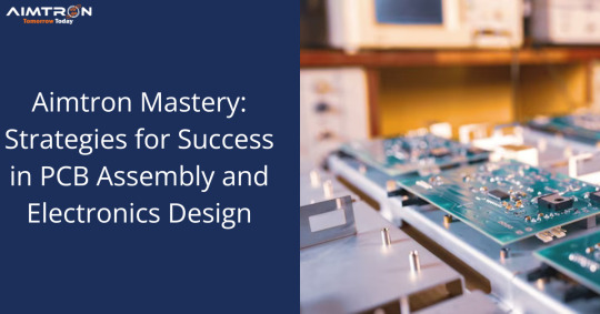
Welcome to the world of Aimtron Mastery, where precision meets innovation in the realm of PCB Assembly and Electronics Design. In this blog, we embark on a journey to unravel the strategies that pave the way for unparalleled success in the intricate world of electronic circuitry.
Navigating the Aimtron Advantage
Introduction to Aimtron: A Game-Changer in Electronics
Aimtron is not just a name; it's a symbol of cutting-edge technology, efficiency, and excellence. Discover how Aimtron's solutions are revolutionizing the landscape of PCB assembly and electronics design, setting new benchmarks for quality and performance.
Strategies for Seamless PCB Assembly
1. Precision Redefined: Understanding Aimtron's Impact
Delve into the nuances of precision in PCB assembly. Explore how Aimtron redefines the standards, offering insights into achieving flawlessness in every solder joint, component placement, and assembly process.
2. Efficiency Unleashed: Optimizing Workflow with Aimtron
Learn the secrets of streamlining your workflow with Aimtron's advanced techniques. From design validation to prototyping, we explore how Aimtron enhances efficiency at every stage of PCB assembly.
3. Future-Proofing Designs: The Aimtron Approach
Anticipate tomorrow's challenges today. Uncover the strategies employed by Aimtron to future-proof your electronics designs, ensuring adaptability and longevity in a rapidly evolving technological landscape.
Innovative Approaches to Electronics Design
1. Beyond the Basics: Advanced Electronics Design Techniques
Move beyond conventional design methodologies. Explore the advanced techniques Aimtron employs in electronics design, pushing the boundaries of creativity and functionality.
2. Aimtron Chronicles: Real-world Applications and Success Stories
Dive into the Aimtron Chronicles, where real-world applications and success stories showcase the transformative power of Aimtron in electronics design. Learn from industry leaders and innovators who have mastered the art of electronic circuitry.
3. The Art and Science of Electronics: Balancing Aesthetics and Functionality
Discover the delicate balance between aesthetics and functionality. Aimtron Mastery goes beyond technicalities, exploring how to create electronics designs that are not only efficient but also visually appealing.
Embark on Your Aimtron Journey
1. Aimtron Insights: Expert Tips and Tricks
Unlock a treasure trove of expert tips and tricks. Whether you're a seasoned professional or a budding enthusiast, Aimtron Insights provides valuable nuggets of wisdom to enhance your skills and stay ahead in the game.
2. Aimtron Community: Joining Forces for Excellence
Connect with like-minded individuals in the Aimtron Community. Share experiences, seek advice, and collaborate on projects. The Aimtron Mastery journey is more enriching when shared with a community that values excellence.
Embark on your Aimtron Mastery journey today and witness the transformation of your PCB assembly and electronics design endeavors. Stay tuned for regular updates, deep dives into Aimtron technologies, and expert insights that will propel you towards success in this ever-evolving field.
0 notes
Text
Printed Circuit Board Manufacturers
Introduction
In today's technological landscape, printed circuit boards (PCBs) are at the heart of countless electronic devices. Whether it's smartphones, computers, or medical equipment, PCBs play a critical role in connecting and powering various components. When it comes to choosing a PCB manufacturer, it's essential to find a reliable partner that can meet your specific requirements. In this article, we will explore the top 4 PCB manufacturers in the USA, highlighting their strengths and capabilities.
What is a PCB?
Before diving into the details, let's briefly understand what a PCB is. A printed circuit board is a flat board made of non-conductive material, usually fiberglass, with copper tracks etched or printed onto it. These tracks serve as electrical pathways, connecting different electronic components such as resistors, capacitors, and integrated circuits. PCBs provide mechanical support and facilitate the efficient flow of electrical signals, making them vital in modern electronic devices.
Importance of choosing the right PCB manufacturer
Choosing the right PCB manufacturer is crucial for the success of any electronic product. The quality, reliability, and performance of the PCB can significantly impact the overall functionality and longevity of the device. A reputable manufacturer ensures that the PCBs are manufactured to meet industry standards, undergo thorough testing, and are built to withstand various environmental conditions.
Factors to consider when choosing a PCB manufacturer
When selecting a PCB manufacturer, several factors should be taken into consideration:
Quality and reliability: Look for manufacturers with a track record of producing high-quality and reliable PCBs. Quality control measures, certifications, and adherence to industry standards are indicators of a manufacturer's commitment to excellence.
Manufacturing capabilities: Assess the manufacturer's manufacturing capabilities, including equipment, production capacity, and technological expertise. This ensures they can handle your specific project requirements effectively.
Technical support and customer service: Good technical support and responsive customer service are invaluable when it comes to resolving any issues or addressing concerns throughout the PCB manufacturing process.
Pricing and lead times: Evaluate the manufacturer's pricing structure and lead times to ensure they align with your project budget and timeline. Balancing cost-effectiveness with timely delivery is crucial.
Visit for more information on PCB Manufacturers: https://www.acmecircuit.com/blog/
#PCBManufacturers#PCBManufacturing#PrintedCircuitBoard#CircuitBoardAssembly#CircuitBoardManufacturing#PCBBoardManufacturer#HighFrequencyPCB#PCBManufacturersNearMe#PCBManufacturer#PCBSupplier#PCBAssemblyServices#PCBAssemblyManufacturer#ElectronicCableAssembly#ElectronicContractServices#PCBExporters#PrintedCircuitBoardManufacturer#PCBManufacturingCompanies#PCBManufacturerIndia#PCBIndustry#PCBSolutions#ElectronicManufacturing#PCBPrototyping#PCBDesign#ElectronicsProduction#PCBQualityControl#ElectronicsEngineering#PCBTechnology#PCBExperts#PCBInnovation#PCBManufacturingProcess
0 notes
Text
Look no further than Acme! Our cutting-edge technology and expert team deliver high-quality PCBs that will exceed your expectations.
Trust us to bring your designs to life. Discover more about our services now!
Visit: https://www.acmecircuit.com/
#printedcircuitboardmanufacturers#electroniccableassembly#pcbmanufacturing#electroniccontractservices#pcbassemblyservices#pcbassemblymanufacturer#pcbexporters#pcbboardmanufacturer#printedcircuitboardmanufacturerinindia#circuitboardmanufacturing
1 note
·
View note
Text
Top PCB Manufacturers In India

https://www.acmecircuit.com Are providers of top quality printed circuit board suppliers, printed circuit board manufacturers & rigid boards suppliers, etc at the industrial level at reasonable rates. For more info please contact us at (+91 98980 11524)
#PCBManufacturers#PCBManufacturing#PrintedCircuitBoard#CircuitBoardAssembly#CircuitBoardManufacturing#PCBBoardManufacturer#HighFrequencyPCB#PCBManufacturersNearMe#PCBManufacturer#PCBSupplier#PCBAssemblyServices#PCBAssemblyManufacturer#ElectronicCableAssembly#ElectronicContractServices#PCBExporters#PrintedCircuitBoardManufacturer#PCBManufacturingCompanies#PCBManufacturerIndia#PCBIndustry#PCBSolutions#ElectronicManufacturing#PCBPrototyping#PCBDesign#ElectronicsProduction#PCBQualityControl#ElectronicsEngineering#PCBTechnology#PCBExperts#PCBInnovation#PCBManufacturingProcess
1 note
·
View note
Text
Physical and Electrical Partitioning In PCB Design
Partitioning your design into physical and electrical sections can significantly reduce the number of through-holes you need in your PCB, thereby increasing production speed and cutting down on manufacturing costs. Here, we will explain what physical and electrical partitioning are how they are used in PC design, and how to create effective partitioning schemes in your PCB designs.
As you work on your next PCB design, you may be wondering how to implement physical and electrical partitioning in your design. These two factors are equally important to making the finished product successful, and both have a huge impact on the success of your design project as a whole. Stay with us if you’re looking to save time and money while producing high-quality products, read on!
Layout Considerations
When you’re laying out a Printed Circuit Board, you have two different considerations, such as physical, which is how your components are laid out on your printed circuit board; and electrical, which has to do with where you're going to put all of your wires. These two can be grouped when it comes time for assembly.
For example, if you plan to use surface-mount parts that require soldering instead of wire-wrapping, then you will want to make sure that there is enough space between these parts so that they can be easily soldered onto your PCB. If you don’t leave enough space between them, then there won’t be room for solder paste. The solder paste is a sticky substance used to hold down SMT parts during pcb assembly.
This makes soldering difficult or impossible and the same logic applies to wiring. If you don’t leave enough space between components, then your wires may not fit without being bent too much or getting in each other’s way. This can cause problems when it comes time to solder everything together, as well as with heat dissipation, and too many wires crammed into one area might block airflow and cause overheating issues.
On top of that, you also need to consider things like trace width and spacing. Trace width refers to how wide your traces are (the lines connecting individual pads on your PCB), while trace spacing refers to how far apart they are from each other. Trace width should always be smaller than trace spacing because having wider traces means more copper is needed per unit length which means higher cost and greater weight.
Traces are usually made using either a single solid line or multiple lines connected by vias. Single solid lines tend to be faster but less reliable than multiple lines connected by vias, but they’re also easier to design and cheaper. Vias are holes drilled through layers of material that allow traces on different layers to connect.However, vias increase complexity and cost. There are several tools available to help designers create their circuits. Some free software options include EagleCAD, Kicad, Altium Designer, and CAD. However, regardless of what software you choose to use, remember that layout is only half of the process.
Overlapping Impedance Nets & Ghost Nets
To create a circuit board with electrical & physical separation, you must insert impedance nets into your design. There are three different ways you can do that, including overlapping impedances, creating ghosts, or through a virtual ground plane. In some designs, more than one method is used. So, let’s see how and when to use them.
An overlapping impedance net has part of it on one side of a barrier, and part of it on another side. A ghost net is used when you have two nets that need to be separated but you don't want them physically separated because they are too close together or because they are too important for each other. A ghost net is just a virtual representation of an actual physical connection that exists between two parts of your circuit board.
A good example of why you might use a ghost PC board net instead of separating your nets with some physical method is if you have 2 power supplies that need to share ground. They can share ground by having their grounds tied together through some kind of wire.But, since they're both supplying power independently, we don't want them tied directly together at all times, but only when there is a current going through either one or both supplies. So what do we do? We create a ghost ground plane where we tie their grounds together. This way, when none ofthe supplies is active, there's no connection between them, and when either supply is active, there isa connection between them.
An electrical partitioning net does exactly what it sounds like. It partitions electrical signals from each other. In a design where you want to physically separate your nets, you can do that by creating an impedance plane that separates them. But, then how do you keep them electrically isolated? That's where a physical partitioning plane comes into play. This is just another name for a ghost ground plane, but instead of being used for sharing grounds between two supplies, it's used for keeping two parts of your circuit board electrically isolated from each other while still allowing communication between them.
One last thing about these three methods is thatyou can't use one without using at least one of the others. If you have a wall between two sections of your circuit board, there has to be some way for those sections to talk to each other. Otherwise, they wouldn't be able to pass power or data. So, if you have a wall, you need ghosts or an impedance plane on both sides of it. And if you have ghosts, there needs to be a wall somewhere too.
Why Would You Ever Choose One Method Over Another?
Well, overlapping impedances are good when you don't need high-frequency performance because they introduce more inductance than either of the other two methods. Ghosts are good when you don't care as much about electromagnetic interference or EMI because they don't create as much capacitance as either of the other two methods.
Whereas the physical partitioning nets are good when you want to keep your layout compact or if you have a design that's already laid out and you can't change it, as having a wall between two sections of your board is going to require some rework if it doesn't already exist.
So, you need to decide if you want your partitions at a high frequency or low frequency. For a high-frequency circuit board, you'll need to use overlapping impedances or ghosts; for a low-frequency circuit board, you can just go with physical partitioning nets.
Solving Unplanned Overlaps
It’s not uncommon for two different circuit boards or two different designs within a single board to overlap. Unplanned overlaps are hard to solve, but these tips will help you create better schematics so that you can avoid them.
Before you design your next PCB, make sure you follow all of these guidelines for PC Board Fabrication. By doing so, you’ll be able to identify overlaps before they occur and reduce your chances of creating any issues when manufacturing your product.
If you don’t have access to specialized tools or software, consider using some online tools like Google Sketch Up to help with your schematic design. These free programs allow you to build 3D models of your circuits, as well as export them into other applications like Eagle CAD or Altium Designer. This allows you to easily view how your components will fit together on a printed circuit board.
You should also use both software and hardware layout techniques to ensure that there aren’t any unplanned overlaps between your PCBs. While it may seem easier to just use one method, it’s important to understand how each technique works so that you can spot potential problems early on. For example, if you only use software-based layout techniques, then you might miss physical overlaps that would prevent a component from fitting onto your board.
Similarly, if you only rely on hardware-based methods, then you might overlook electrical conflicts that could lead to shorts or failures during testing. The best way to get around these kinds of issues is by using both types of layouts simultaneously. You can use a program like Altium Designer to lay out your circuit board, then print out an image of what you’ve created. Then take that printed image and place it over your actual PCB. This ensures that you catch any unplanned overlaps before they cause problems later on down the line.
Just remember, even though it takes more time upfront, double-checking everything twice is always worth it. With that said, there are still times when the overlap errors do slip through. When you find yourself in a situation where you need to resolve an issue like this, we recommend you double-check it. As it would become much easier to fix an error than it would be otherwise. You can also get professional help in this regard.
Would like to know more about physical and electrical partitioning in your designs or pcb assembly services? Write us at [email protected]
Website: https://pnconline.com/
Facebook: https://www.facebook.com/PNCONLINE
Twitter: https://twitter.com/PNCINC
Instagram: https://www.instagram.com/pnc_pcb/
Tumblr: https://www.tumblr.com/blog/view/pncinc
Myspace :https://myspace.com/pncinc2020
Bresdel: https://bresdel.com/pncinc
Call us: (973) 284-1600
Email us: [email protected]
Location: PNC INC, 115 East Centre St.Nutley, NJ, 07110
0 notes
Text
Tips for RF PCB Design
With so many things to consider when designing an RF PCB, it can be hard to know where to start. How do you choose the right layout? What tools should you use to get the job done? RF PCB design has its own set of challenges that need to be addressed to get the most out of your circuit. There are some best practices you can use to ensure that your design will function optimally and run smoothly.
The best PCB design solution can be the difference between success and failure for your product, so you want to make sure that you are getting it right the first time around. Our guide will walk you through all of the steps necessary to create an RF design that works and that makes your product even better than you envisioned.
Surface Mount Capacitors
Use surface mount capacitors when space is limited. You can incorporate them into your RF Printed Circuit Board design with no impact on performance. Try to keep track of how much space they’ll take and make sure there’s still enough room for other components on the board, like resistors and coils. The surface mount parts are more fragile than through-hole components and require an extra level of care when handling.
Consider using larger surface mount parts wherever possible, or incorporating test points into any sensitive areas if smaller parts are required. Remember that small surface-mount parts have very thin leads that could break off easily. Make sure you know what size of solder tip will be needed before moving forward with your design. If it’s too small, it could damage the delicate leads on these devices. It may also be difficult to attach them to boards after soldering as their leads are so small that they tend to slide around during assembly. When in doubt, use a slightly larger part.
Differential Pair Transformer Coupling
Choosing proper circuit components is an important part of designing and building circuits. When creating transmitter/receiver pairs, several factors influence how well each device will perform. The goal of any transmitter or receiver circuit is to accurately convert an input voltage into an output voltage with minimal noise and distortion.
These parameters are known as gain, linearity, bandwidth, noise figure, NF, return loss, RL, and intercept point, IP. A low NF results in more power being transferred from input to output. The IP value represents how much power can be handled by the front end of a given device before distorting or saturating it, all while maintaining its linearity characteristics.
In other words, if a device has high gain but poor linearity, then it may still have acceptable levels of IP. But if a device has high gain and poor linearity at lower power levels, then it won’t have good IP numbers. In general, devices with higher gains have lower bandwidths, however, there are exceptions to every rule. For example, some amplifiers have very high gains but also operate over wide frequency ranges.
Microstrip Transmission Lines
These are transmission lines in which all of their circuit elements, including those forming half-space planes, and terminations, such as capacitors and transformers, are fabricated on metal strip circuits. The strip circuit is usually etched onto an epoxy substrate using photo etching or electroplating techniques. The micro-strip designs have become very popular for many PC BOARD applications because they can be packaged in small cases with relative ease due to their thin profile. They also have good impedance matching properties over a wide frequency range.
Reference Planes, Power Planes & Ground Planes
Radio-frequency circuit boards or RF designs are often more sensitive to ground loops and signal integrity issues than regular designs because RF circuits and components are particularly susceptible to noise. One way that experienced designers combat these types of issues is by strategically adding power planes, reference planes, and ground planes to their board layouts.
Reference planes: The reference or signal planes can allow designers to focus on specific sections of a circuit without having to worry about interfering signals from other portions.
They also provide a convenient place for designers to add vias between layers of copper, which helps improve both signal quality and thermal performance. Reference planes can be especially useful when they’re directly connected to a component’s ground pin, which allows them to act as an extension of that component’s ground plane.
Power planes: They should always be connected directly to an external source of power, otherwise, they could cause voltage drops across adjacent traces and components.
Ground planes: They should always be connected directly to an external source of the earth, otherwise, they could cause the voltage rises across adjacent traces and components. It's important to note that many high-speed applications use multiple ground planes at different potentials, so it may not be feasible to have just one global ground plane. However, it's generally best practice to keep each section within a single board connected through at least one shared global ground plane.
By using separate grounds for different sections of a design, designers can avoid parasitic effects and increase the overall reliability by ensuring all parts of their designs have access to low impedance paths back to an external earth point.
In addition, it’s crucial to ensure that any ground or power planes are spaced far enough away from any active circuitry in order to minimize crosstalk. Generally speaking, there should be at least 1/10th of a millimeter between active circuitry and any nearby reference or power planes. The distance requirements become even more stringent with higher frequencies. When operating above 30 GHz, there should ideally be no less than 0.3 mm of separation between any ground or power plane and active circuitry.
Vias – Size, Shape & Placement
Vias are required in order for us to make electrical contact with traces on different layers. There are three types of vias, including plated through, blind, and buried. A plated through via connects one layer’s copper trace directly with another via’s copper trace or traces. A blind via creates electrical contact but no physical connection between two layers and a buried via provides both an electrical and physical connection.
Placement is generally determined by where it will be soldered or how many layers are involved. For example, if there are four or more layers involved then we recommend using plated through vias because they offer better conductivity than a blind via. If there are only two layers involved then we recommend using either type of visa, depending on its location relative to other components.
As far as shape goes, choose from square, round, or rectangular options that match your pcb fabrication layout requirements. Circular vias may also be available upon request, however, these have a higher cost associated with them due to their complexity and are not always necessary. We use wire-bondable vias wherever possible because they provide a faster assembly process. The above diagram illustrates each type of via along with its respective shape and size.
Isolating an RF trace
It is essential to isolate an RF trace from high-speed signals, including HDMI, USB differential pairs, or crystals’ clock traces. Experts do it through a method known as via stitching where vias are stitched around the RF traces to keep them away from other parts on the circuit board. But, there should be proper isolation as improper isolation can affect PCB function.
RF Circuit Board Insulation
Insulation is one of the most important factors for minimizing the signal loss in an RF transmission. If you want to ensure that your signal reaches its destination without any hiccups or interference, it’s crucial that you use good quality material for your board's insulation, and choose one with at least 5-mil thickness.
One of our favorite options is Taconic TFEP as it offers superior heat resistance and can withstand temperatures as high as 350 degrees Celsius. It also has great mechanical properties and will last for years to come. Another great option is Rogers, which boasts similar properties but has a slightly higher temperature resistance.
You'll also want to make sure that you're using a good adhesive when attaching components to your board. This will ensure that everything stays intact even in tough conditions. If you want to ensure that your signal reaches its destination without any hiccups or interference, it’s crucial that you use a good, quality material for your board's insulation.
You can create a flawless RF circuit board by considering all the above design guidelines.
Final Thoughts
RF PCB design has its own set of challenges that need to be addressed in order to get the most out of your circuit. There are some best practices you can use to ensure that your design will function optimally and run smoothly. You have to consider material, traces, surface mount capacitors, isolation, insulation, reference, ground, and power planes, vias size and shape, coupling, and micro-strip transmission line.
Would like to know more about RF design or pcb assembly services? Email us at [email protected]
Website: https://pnconline.com/
Facebook: https://www.facebook.com/PNCONLINE
Twitter: https://twitter.com/PNCINC
Instagram: https://www.instagram.com/pnc_pcb/
Tumblr: https://www.tumblr.com/blog/view/pncinc
Myspace :https://myspace.com/pncinc2020
Bresdel: https://bresdel.com/pncinc
Call us: (973) 284-1600
Email us: [email protected]
Location: PNC INC, 115 East Centre St.Nutley, NJ, 07110
0 notes
Text
Aimtron’s Integrated Approach: PCB Assembly and Electronics Design
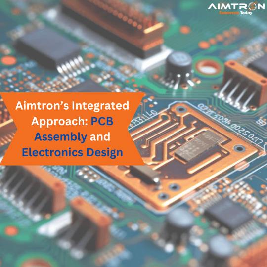
In the ever-evolving landscape of electronics manufacturing, companies seek innovative solutions that seamlessly integrate design and production processes. Aimtron, a leading PCB assembly manufacturer and electronics design firm, stands out for its holistic approach. Let’s delve into how Aimtron achieves this integration and the benefits it brings to its clients.
1. Synergy Between PCB Assembly and Electronics Design
Aimtron recognizes that successful product development requires a harmonious collaboration between PCB assembly and electronics design. Their teams work closely from the initial concept to the final product, ensuring alignment at every stage. By bridging the gap between design and manufacturing, Aimtron minimizes errors, reduces time-to-market, and enhances overall efficiency.
2. Seamless Transition from Design to Production
Aimtron’s integrated approach streamlines the transition from design to production. Their electronics designers understand the intricacies of PCB assembly, considering factors like component placement, trace routing, and manufacturability. This knowledge informs their design choices, resulting in layouts optimized for efficient assembly and reliable performance.
3. Concurrent Engineering for Faster Iterations
Concurrent engineering is at the heart of Aimtron’s approach. Their design and assembly teams collaborate in real time, allowing for rapid iterations. When design changes are necessary, they can be implemented seamlessly without disrupting the production process. This agility accelerates product development cycles and ensures that design improvements are promptly incorporated.
4. Design for Manufacturing (DFM) Principles
Aimtron emphasizes DFM principles throughout the design phase. By considering manufacturing constraints early on, they prevent costly redesigns and delays. DFM practices include selecting components with long lead times, optimizing panelization, and adhering to industry standards. Aimtron’s commitment to DFM ensures that designs are not only functional but also manufacturable.
5. Value-Added Services
Beyond PCB assembly and electronics design, Aimtron offers value-added services. These include prototyping, testing, and supply chain management. Clients benefit from a comprehensive solution that covers the entire product lifecycle. Aimtron’s expertise extends beyond the technical aspects, encompassing project management and customer support.
6. Quality Assurance and Continuous Improvement
Aimtron maintains rigorous quality control processes. Their integrated approach allows for better traceability, as design decisions are directly linked to production outcomes. By continuously analyzing data and feedback, Aimtron identifies areas for improvement and implements corrective actions. The result is consistent quality and customer satisfaction.
7. Customization and Flexibility
Aimtron understands that each project is unique. Their integrated approach allows for customization and flexibility. Whether it’s a complex multilayer PCB or a specialized electronic module, Aimtron adapts its processes to meet specific requirements. Clients appreciate the personalized attention and tailored solutions.
Conclusion
Aimtron’s integrated approach bridges the gap between PCB assembly and electronics design. By fostering collaboration, emphasizing DFM, and maintaining high-quality standards, Aimtron delivers exceptional results. As technology continues to evolve, Aimtron remains committed to innovation, ensuring that their clients’ products thrive in a competitive market.
#pcbassembly#pcbassemblyservice#pcbassemblymanufacturer#electronicsdesign#pcbdesign#electronicsmanufacturing#electronicsmanufacturingservice
0 notes
Last Seen Blogs


q742v8k9d
바카라타이배당FM821COM 바카라종류 바카

laymanvaper-blog
The Layman Vaper

rwnjun
tamquam alter idem

sillyzippersportstoad
Untitled