#EDAtools
Explore tagged Tumblr posts
Visit Tumblr Blog
Explore Tumblr blogs with no restrictions, modern design and the best experience.
Last Seen Tumblr Blogs


Fun Fact
Users from the US are the majority of Tumblr visitors.
Text
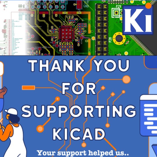
Giving Tuesday – KiCad open-source design #GivingTuesday 💻🔧🌍❤️🤝
KiCad is an open-source software suite for electronic design automation (EDA), enabling users to design schematics and printed circuit boards (PCBs). KiCad is a great, free, open tool for creating complex designs, from hobbyist projects to professional-grade hardware. As an open-source initiative, KiCad promotes accessibility and collaboration, making advanced EDA tools freely available. Supporting KiCad helps the development of features, bug fixes, and community-driven improvements, empowering engineers, educators, and hobbyists worldwide. Consider donating to KiCad to strengthen the open-source hardware community and help make high-quality EDA tools accessible to everyone.
In the past year, they posted this nifty chart that shows what your support can help accomplish.

If KiCad is valuable to you, please consider donating to help make it even better.
#kicad#kicadpcb#electronics#eda#schematic#pcbdesign#pcblayout#opensource#edatools#openhardware#donatetoday#engineeringdesign#communitysupport#openedsystems#opensourcecommunity#pcbtools#givingback#generositymatters#techforgood#makercommunity#electronicsdesign#designsoftware#kicaddonation#hardwaredesign#opensourceinitiative#techcommunity#sharekindness
11 notes
·
View notes
Text

🧠 QUIZ TIME
What is a main goal of EDA ?
A. Model Training B. Data Encryption C. Deployment D. Data Visualization
EDA helps us understand the structure of data, identify patterns, and make informed decisions before model building.
✅ Why Choose Us?
✔️ 100% practical training
✔️ Real-time projects & case studies
✔️ Expert mentors with industry experience
✔️ Certification & job assistance
��️ Easy-to-understand Telugu + English mix classes
📍 Institute Address:
3rd Floor, Dr. Atmaram Estates, Metro Pillar No. A690,
Beside Siri Pearls & Jewellery, near JNTU Metro Station,
Hyder Nagar, Vasantha Nagar, Hyderabad, Telangana – 500072
📞 Contact: +91 9948801222
📧 Email: [email protected]
🌐 Website: https://dataanalyticsmasters.in
#DataAnalytics#EDA#ExploratoryDataAnalysis#DataVisualization#DataScienceQuiz#QuizTime#AnalyticsTraining#DataAnalyticsCourse#LearnDataScience#DataScienceBasics#DataAnalyticsMasters#EDATools#HyderabadInstitute#JoinNow#CareerInDataScience
0 notes
Text
Smarter VLSI Design Through AI-Powered Innovation
As semiconductor technology continues to evolve, the demand for high-performance and energy-efficient chips is reshaping how integrated circuits are designed. Traditional VLSI (Very-Large-Scale Integration) methods, while foundational, are becoming insufficient for the scale and complexity of modern electronics. To bridge this gap, Artificial Intelligence (AI) is being integrated into VLSI design workflows — unlocking smarter, faster, and more optimized chip development.
Tech4BizSolutions is actively leveraging AI to enhance every stage of the VLSI lifecycle, from architecture planning to post-silicon validation.

What Is AI-Driven VLSI Design?
AI-driven VLSI design refers to the application of machine learning, deep learning, and data analytics to automate and optimize various stages of chip design and manufacturing. Unlike conventional design flows, AI can identify patterns, predict outcomes, and generate insights from massive datasets in real-time.
Key advantages include:
Improved performance-to-power ratio
Reduced manual effort in layout planning
Faster design rule checking and validation
Enhanced yield prediction and fault analysis
Tech4BizSolutions integrates AI across multiple design layers, reducing time-to-market while improving design accuracy and production reliability.
How Tech4BizSolutions Enhances VLSI with AI
At Tech4BizSolutions, we fuse our deep domain knowledge in semiconductor design with cutting-edge AI techniques. Here’s a breakdown of how we apply AI to make VLSI smarter:
1. AI in Design Space Exploration
Design space exploration is one of the most time-consuming phases of VLSI. Our AI models intelligently evaluate thousands of possible configurations, identifying the most efficient architecture with minimal resource usage.
Tech4BizSolutions Result: Up to 50% reduction in time spent exploring design alternatives.
2. Automated Floorplanning and Layout Optimization
Floorplanning and placement affect timing, area, and power consumption. We use neural networks to predict optimal component placement and signal routing paths, reducing congestion and delay.
Tech4BizSolutions Advantage: Increased chip efficiency with reduced layout iterations.
3. AI-Enhanced Timing and Power Analysis
Tech4BizSolutions uses AI models trained on historical data to predict timing violations and power bottlenecks before physical implementation. This allows early-stage corrections, saving time and silicon costs.
Outcome: More accurate PPA (Performance, Power, Area) metrics at the RTL level.
4. Fault Detection and Yield Improvement
AI helps detect subtle, non-obvious design flaws by recognizing patterns in simulation and test bench outputs. We also use AI to simulate rare corner cases that are typically missed in standard verification cycles.
Business Impact: Higher first-pass silicon success rates and lower manufacturing risks.
5. Adaptive Learning Systems for Continuous Optimization
Our AI systems are not static. They learn and evolve with every project. We build feedback loops where post-silicon data refines future simulations and models — creating a smarter design pipeline over time.
Long-term Benefit: Each new chip design becomes more efficient than the last, reducing NRE (Non-Recurring Engineering) costs.
Tech4BizSolutions: Delivering Tangible Business Value
By embedding AI into VLSI design workflows, Tech4BizSolutions helps clients:
Speed up development cycles by up to 40%
Reduce power consumption by designing for energy-aware applications
Increase IC performance through AI-informed microarchitecture tuning
Minimize silicon iterations and time spent on debugging
Predict and eliminate faults before tape-out
This makes our approach ideal for industries like:
Consumer Electronics
Automotive & EV
Industrial Automation
Telecom and 5G
IoT and Edge Devices
Real-World Use Case
Let’s say a client needs a custom AI accelerator chip for real-time video processing. With traditional VLSI design, modeling workloads, optimizing for latency, and reducing power draw can take months.
With Tech4BizSolutions’ AI-enhanced VLSI flow, we:
Use AI models to simulate expected video processing loads
Automatically adjust component placement for thermal efficiency
Predict the power envelope across real-world scenarios
Validate logic paths using AI-driven test vectors
Result: A custom ASIC delivered 30% faster with optimized performance and reliability.
Conclusion: The Future of Smarter Chip Design Starts Here
VLSI design is undergoing a significant transformation. As chip complexity continues to rise, integrating AI into every stage of the design and manufacturing process is not just an option — it’s a necessity.
Tech4BizSolutions is proud to lead this evolution with intelligent VLSI design solutions that are adaptive, efficient, and future-ready. Our AI-infused approach ensures not only faster development but smarter chips that can meet the demands of modern, connected, and data-driven applications.
Whether you’re building the next-gen smart device or need custom silicon for industrial systems, Tech4BizSolutions has the tools, talent, and technology to deliver.
Want to learn how AI can power your next chip design?
Contact Tech4BizSolutions today and explore the possibilities of intelligent VLSI.
#VLSIDesign#AIDrivenDesign#SemiconductorInnovation#ChipDesign#Tech4BizSolutions#HardwareInnovation#ASICDesign#EDAtools#DesignAutomation#TechSolutions#PowerEfficientDesign#CustomChipDesign
0 notes