#Flip Chip Technology Market
Explore tagged Tumblr posts
Visit Tumblr Blog
Explore Tumblr blogs with no restrictions, modern design and the best experience.
Last Seen Tumblr Blogs


Fun Fact
The most popular pages on Tumblr are about Minecraft, GIFs, and David J. Peterson.
Text
Dimensity 7300 : Unbelievable Speed and Power Unleashed
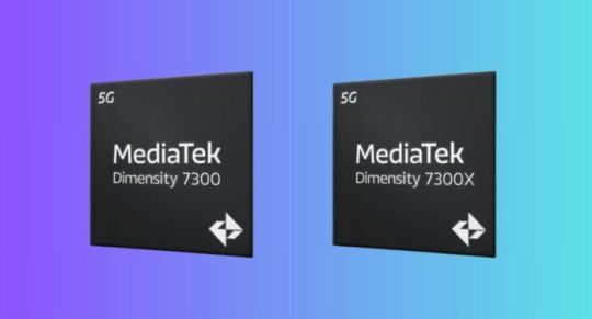
MediaTek launched the 4nm Dimensity 7300 and Dimensity 7300X high-end mobile device processors today. Best-in-class power economy and performance make Dimensity 7300 chipsets ideal for AI-enhanced computing, faster gaming, better photography, and effortless multitasking. Dimensity 7300X supports twin displays for flip-style foldable devices.
Both MediaTek Dimensity 7300 chipsets have 2.5GHz octa-core CPUs with 4X Arm Cortex-A78 and A55 cores. 4nm reduces A78 core power consumption by 25% over Dimensity 7050. To speed up gaming, the CPU combines the most recent Arm Mali-G615 GPU with a number of MediaTek HyperEngine optimisations. The Dimensity 7300 series provides 20% quicker FPS and 20% more energy efficiency than competing options. The new chips optimise 5G and Wi-Fi game connections, use clever resource optimisation, support Dual-Link True Wireless Stereo Audio and Bluetooth LE Audio technology to significantly improve gaming experiences.
According to MediaTek’s Wireless Communications Business Deputy General Manager Dr. According to Yenchi Lee, “The MediaTek Dimensity 7300 chips will help integrate the newest AI and connectivity technologies consumers can stream and game seamlessly. “Furthermore, the dual display capability of the Dimensity 7300X allows OEMs to create creative new form factors.”
With compatibility for a 200MP primary camera and a premium-grade 12-bit HDR-ISP, the MediaTek Imagiq 950 is another enhanced photographic feature available with the Dimensity 7300 chipsets. New hardware engines provide accurate noise reduction (MCNR), face detection (HWFD), and video HDR in the Dimensity 7300. This allows users to take beautiful pictures and videos in any kind of lighting. Compared to the Dimensity 7050, live focus and photo remastering are 1.3X and 1.5X faster, respectively. In addition, 4K HDR video may be recorded with a dynamic range that is more than 50% broader than competing solutions, allowing users to capture more detail in their recordings.
The MediaTek APU 655 doubles the performance of the Dimensity 7050 while also greatly increasing the efficiency of AI tasks. Also, in order to reduce memory requirements for larger AI models and more effectively use memory bandwidth, the Dimensity 7300 chips support new mixed precision data types.
The Dimensity 7300 SoCs enable global HDR standards and remarkably detailed WFHD+ displays with 10-bit true colour thanks to MediaTek’s built-in MiraVision 955. This improves media streaming and playing. Additionally, OEMs find it simpler to satisfy the expanding market demand for cutting-edge form factors thanks to the Dimensity 7300X’s specialised support for dual display flip phones.
Dimensity 7300 and Dimensity 7300X important features
With MediaTek’s own optimisations and a full suite of R16 power-saving advancements, MediaTek 5G UltraSave 3.0+ technology offers 13–30% more power efficiency than competing options in typical 5G sub-6GHz connectivity settings.
Supporting 3CC carrier aggregation up to 3.27Gb/s 5G downstream speed, which enables better downlink rates in suburban and urban settings.
Support for multi-band Wi-Fi 6E allows for dependable and quick multi-gigabit wireless access.
Users will have more options with dual 5G SIM capability and dual VoNR.
This was addressed by MediaTek’s Dimensity 7300 series in May 2024. The Dimensity 7300 and 7300X chipset series boosts high-end to smartphone and foldable device performance, energy efficiency, and AI.
Constructed for Rapidity and Effectiveness
A powerful octa-core CPU powers the Dimensity 7300. This combo is ideal for gaming and multitasking with four 2.5 GHz Arm Cortex-A78 cores. Four Arm Cortex-A55 cores, which are energy-efficient, complement these and guarantee dependable performance for daily use. In comparison to the Dimensity 7050, this combination represents a major advancement.
The advanced 4nm manufacturing process is a feature of the 7300 series. This corresponds to a 25% decrease in power usage over the 6nm technique utilised in earlier generations. Users will benefit from longer battery life as a result, while manufacturers can create sleeker devices without compromising functionality.
Superpower in Graphics
Immersive mobile experiences require strong visuals. The Dimensity 7300 has an Arm Mali-G615 GPU to fix this. This graphics processor runs even the most demanding games smoothly, and MediaTek’s HyperEngine technology stabilises the network and efficiently manages resources. MediaTek says the 7300 series is appealing to mobile gamers due to its 20% higher frame rates (FPS) and energy economy.
AI Gains Strength
AI is increasingly changing the smartphone experience, enabling intelligent assistants, better photography, and facial recognition. The Dimensity 7300 uses the MediaTek APU 655, following this trend. This AI processing unit doubles the efficiency of the Dimensity 7050, resulting in a notable performance boost. New mixed precision data types, which enable more effective memory bandwidth utilisation and lower memory requirements for larger AI models, are also supported by the 7300 series. Future smartphones will be able to incorporate even more advanced AI features thanks to this.
Gorgeous Images
For a fascinating mobile experience, a stunning display is essential; a strong processor is only half the story. This demand is met by the Dimensity 7300 series, which supports powerful screens. With the ability to support WFHD+ resolutions at frame rates of up to 120 Hz, these chipsets guarantee fluid and visually spectacular images. For an even smoother user experience, the 7300 series also supports Full HD+ screens at an even higher refresh rate of 144Hz.
Concentrate on Take Pictures
Users now place a greater value on mobile photography, and the Dimensity 7300 series delivers. The chip has MediaTek’s Imagiq 950 image signal processor (ISP), which provides sophisticated photographic features. With the 12-bit HDR pipeline supported by this ISP, detailed information and brilliant colours may be captured. Furthermore, the Imagiq 950 enables features like video HDR, face detection, and precise noise reduction, guaranteeing beautiful images and movies in a range of lighting scenarios. The 7300 series stands out for its ability to enable dual simultaneous video capture, which allows for the development of more imaginative content.
A Set of Chips for Foldables
A 7300 variation called the Dimensity 7300X goes one step farther by being designed with foldable cellphones in mind. One essential component of these cutting-edge gadgets is dual display compatibility, which this chipset provides. Manufacturers may design foldable phones with seamless experiences on both the cover and main displays thanks to the 7300X.
Mobile’s Future
Mobile processing power has advanced significantly with the release of the Dimensity 7300 series. This chipset family, with its emphasis on efficiency, performance, AI capabilities, and support for cutting-edge technologies like foldable devices and high refresh rate screens, is positioned to have a significant impact on the direction of mobile technology. The Dimensity 7300 series offers makers a strong and adaptable foundation to develop next-generation smartphones that offer outstanding user experiences as smartphones continue to advance.
Read more on govindhtech.com
#dimensity7300x#MediaTekDimensity#AI#artificialintelligence#AITechnology#mobiletechnology#smartphone#aimodel#CPU#cpupower#news#technews#technology#technologynews#technologytrends#govindhtech
7 notes
·
View notes
Text
0 notes
Text
Semiconductor Bonding Market Size to Hit USD 1,274.8 Billion by 2032

The global semiconductor bonding market industry was valued at USD 959.7 million in 2024 and is projected to grow from USD 991.1 million in 2025 to USD 1,274.8 million by 2032, exhibiting a CAGR of 3.7% during the forecast period. As chip manufacturing transitions into advanced packaging and 3D integration, demand for precise and reliable bonding technologies continues to rise steadily.
Key Market Highlights:
2024 Global Market Size: USD 959.7 million
2025 Global Market Size (Forecast Start): USD 991.1 million
2032 Global Market Size: USD 1,274.8 million
CAGR (2025–2032): 3.7%
Primary Market Focus: Wafer bonding, die bonding, flip chip bonding, hybrid bonding
Core Application Areas: Consumer electronics, automotive electronics, industrial devices, 5G infrastructure, AI processors
Key Players in the Global Market:
Kulicke & Soffa Industries, Inc.
ASM Pacific Technology Ltd.
BESI (BE Semiconductor Industries N.V.)
Shinkawa Ltd.
Panasonic Industry Co., Ltd.
Palomar Technologies
F&K Delvotec Bondtechnik GmbH
TPT Wire Bonder GmbH & Co. KG
Hesse Mechatronics
MRSI Systems
Request Sample PDF: https://www.fortunebusinessinsights.com/enquiry/request-sample-pdf/semiconductor-bonding-market-110168
Covered Dynamics:
Growth Drivers:
Advanced Packaging Demand: Growing use of 3D ICs, chiplets, and fan-out wafer-level packaging
AI and 5G Expansion: Devices require faster interconnects and high-density bonding
Miniaturization Trends: Precision bonding technologies critical for smaller chip architectures
Rise of EVs & ADAS: Semiconductor bonding for automotive-grade reliability
Increased Outsourced Semiconductor Assembly and Testing (OSAT): Greater use of high-throughput bonding systems
Key Opportunities:
Hybrid Bonding Surge: Strong interest from high-performance computing and smartphone chip manufacturers
MEMS Integration: Accelerated use of bonding in micro-electromechanical systems (e.g., sensors, actuators)
Photonics and Optoelectronics: Growth in optical chip bonding for data centers and LIDAR systems
Material Innovation: Opportunities in low-temperature bonding, Cu-Cu bonding, and adhesive-free bonding
Regional Analysis:
Asia Pacific: Dominates global market due to concentration of semiconductor fabs in Taiwan, South Korea, China, and Japan
North America: Home to key technology developers and a growing presence in advanced packaging (especially for defense and AI)
Europe: Focused on automotive-grade semiconductor bonding systems
Technology & Application Scope:
Bonding Types:
Die bonding (epoxy, eutectic, thermocompression)
Wafer bonding (direct, anodic, adhesive, fusion)
Flip chip bonding
Hybrid/3D bonding
End-Use Industries:
Consumer electronics
Automotive
Telecom & datacom
Healthcare (wearables, implants)
Industrial & defense systems
Emerging Technologies:
Chiplets and advanced SoC
High-bandwidth memory (HBM) stacks
Quantum computing components
Compound semiconductor bonding (GaN, SiC)
Speak to Analysts: https://www.fortunebusinessinsights.com/enquiry/speak-to-analyst/semiconductor-bonding-market-110168
Recent Developments:
March 2024 – Kulicke & Soffa launched a next-generation thermocompression bonder targeting AI chip applications, increasing bonding speed by 20%.
September 2023 – BESI partnered with a leading Asian OSAT firm to deliver hybrid bonding systems for mass production of 3D NAND memory devices.
Conclusion:
The global semiconductor bonding market is entering a phase of stable, innovation-driven expansion. While the overall growth rate is modest compared to high-velocity tech sectors, the strategic importance of bonding technologies in enabling next-gen chips ensures sustained demand. With chiplet architectures, heterogeneous integration, and AI computing moving into the mainstream, advanced bonding techniques will play a pivotal role in semiconductor evolution.
Frequently Asked Questions:
1. What is the projected value of the global Semiconductor Bonding market by 2032?
2. What was the total market value of Semiconductor Bondings in 2024?
3. What is the expected compound annual growth rate (CAGR) for the market during the forecast period of 2025 to 2032?
4. Which industry segment dominated the Semiconductor Bonding market in 2023?
5. Who are the major companies operating in the Semiconductor Bonding space?
6. Which region held the largest market share in 2023?
#Semiconductor Bonding Market Share#Semiconductor Bonding Market Size#Semiconductor Bonding Market Industry#Semiconductor Bonding Market Driver#Semiconductor Bonding Market Growth#Semiconductor Bonding Market Analysis#Semiconductor Bonding Market Trends
0 notes
Text
Semiconductor Packaging Capillary Market: Competitive Landscape and Emerging Players by 2025-2032

MARKET INSIGHTS
The global Semiconductor Packaging Capillary Market size was valued at US$ 298.5 million in 2024 and is projected to reach US$ 476.8 million by 2032, at a CAGR of 6.91% during the forecast period 2025-2032. While the broader semiconductor industry was estimated at USD 579 billion in 2022, it’s expected to grow to USD 790 billion by 2029 at a 6% CAGR, creating significant demand for packaging components.
Semiconductor packaging capillaries are precision components used in wire bonding processes for IC and LED packaging. These high-performance capillaries, made from materials like tungsten, titanium or ceramic, enable precise interconnection between semiconductor dies and substrates. The capillaries play a critical role in ensuring reliable electrical connections while maintaining thermal and mechanical stability during packaging operations.
The market growth is driven by expanding semiconductor production capacity worldwide, particularly in Asia, and increasing adoption of advanced packaging technologies. While traditional wire bonding remains dominant, emerging trends like heterogeneous integration and chiplet-based designs are creating new requirements for capillary technology. Key players such as Kulicke & Soffa, Adamant Namiki and SPT are investing in R&D to develop capillaries for finer pitch applications below 15μm, responding to the industry’s miniaturization demands.
MARKET DYNAMICS
MARKET DRIVERS
Growing Demand for Advanced Semiconductor Packaging to Accelerate Capillary Adoption
The semiconductor packaging capillary market is experiencing robust growth driven by the increasing demand for advanced packaging solutions in semiconductor manufacturing. As chip designs become more complex with shrinking transistor sizes and higher pin counts, precision wire bonding using capillaries has become critical. The global semiconductor packaging market, valued at over $30 billion, is projected to expand rapidly with the proliferation of 5G, IoT, and AI applications. Advanced packaging techniques like flip-chip and wafer-level packaging require high-performance capillaries to ensure reliable interconnects with minimal defects. This technological evolution is pushing manufacturers to develop capillary solutions with superior wear resistance and thermal stability to meet the rigorous demands of modern semiconductor fabrication.
Expansion of Automotive Electronics Sector to Boost Market Growth
The automotive industry’s rapid electrification and autonomous driving trends are creating substantial demand for semiconductor packaging capillaries. Modern vehicles incorporate hundreds of semiconductor devices for ADAS systems, infotainment, and powertrain control, requiring reliable wire bonding solutions. The automotive semiconductor market is growing at approximately 8% annually, with electric vehicles requiring 50% more semiconductor content than conventional vehicles. This sector’s stringent quality requirements for automotive-grade components mandate the use of high-precision capillaries capable of withstanding harsh operating conditions. Major automotive chip manufacturers are increasingly adopting ceramic and tungsten capillaries for their superior durability in high-temperature applications, driving market expansion.
Technological Advancements in Capillary Materials to Drive Innovation
Recent breakthroughs in capillary material science are revolutionizing semiconductor packaging processes. Advanced ceramic composites and tungsten alloys now offer improved thermal conductivity and wear resistance, enabling higher bonding speeds and longer tool life. Manufacturers are developing capillaries with specialized tip geometries that can handle ultra-fine pitch bonding below 20 microns, crucial for next-generation chip designs. The development of hybrid capillary designs that combine different material properties is gaining traction, allowing optimized performance for specific packaging applications. These technological advancements are enabling semiconductor manufacturers to push the boundaries of miniaturization while maintaining yield and reliability.
MARKET RESTRAINTS
High Production Costs and Material Constraints to Limit Market Growth
While the semiconductor packaging capillary market shows strong potential, several factors are restraining its expansion. The production of high-performance capillaries requires expensive specialty materials like tungsten and ceramic composites, which account for over 60% of the manufacturing cost. Establishing precision manufacturing capabilities for capillaries with micron-level tolerances demands substantial capital investment in specialized CNC grinding and polishing equipment. Additionally, the limited global supply of high-purity refractory metals creates material procurement challenges, particularly during periods of supply chain disruptions. These cost pressures make it difficult for small and medium-sized packaging facilities to justify upgrades to premium capillary solutions, slowing overall market penetration.
Technical Challenges in Ultra-Fine Pitch Bonding to Create Adoption Barriers
The ongoing miniaturization trend in semiconductor packaging presents significant technical hurdles for capillary manufacturers. As bond pad pitches shrink below 15 microns, conventional capillary designs struggle with wire sweep, bonding consistency, and defect rates. Achieving consistent bond quality at these scales requires capillary tip geometries with sub-micron precision, pushing the limits of current manufacturing capabilities. The transition to copper wire bonding, while cost-effective, introduces additional complications as copper’s hardness accelerates capillary wear. These technical challenges force packaging facilities to make substantial investments in process optimization and defect detection systems, increasing the total cost of ownership for advanced capillary solutions.
MARKET CHALLENGES
Workforce Skill Gap and Training Requirements to Pose Operational Challenges
The semiconductor packaging industry faces mounting challenges in maintaining a skilled workforce capable of optimizing capillary-bonding processes. As packaging technologies advance, operators require specialized training to properly calibrate bonding machines, select appropriate capillary profiles, and troubleshoot complex defect patterns. The industry is experiencing a talent shortage, with retirement attrition rates exceeding 20% in some regions while technical training programs struggle to keep pace with evolving requirements. This skills gap is particularly acute for hybrid bonding applications that combine wire bonding with other interconnect technologies, requiring operators to master multiple process disciplines. Companies must invest heavily in workforce development and knowledge transfer initiatives to maintain production quality.
Supply Chain Vulnerabilities to Impact Market Stability
The capillary market remains vulnerable to supply chain disruptions affecting critical raw materials and manufacturing equipment. Over 70% of tungsten carbide powder, a key capillary material, originates from a limited number of suppliers concentrated in specific geographic regions. Precision grinding machines used for capillary production face long lead times due to complex manufacturing requirements and limited vendor capacity. These supply chain constraints became particularly evident during recent global events, causing production delays and price volatility. The semiconductor industry’s cyclical nature further complicates capacity planning, with demand fluctuations making it difficult to maintain optimal inventory levels of specialized capillary products.
MARKET OPPORTUNITIES
Emerging Heterogeneous Integration Trends to Create New Growth Avenues
The semiconductor industry’s shift toward heterogeneous integration and chiplets presents significant opportunities for capillary manufacturers. Advanced packaging approaches like 3D IC stacking and system-in-package designs require innovative interconnect solutions that combine wire bonding with other technologies. There is growing demand for specialized capillaries capable of handling mixed wire types (gold and copper) and bonding to diverse surfaces (organic substrates, silicon interposers). The chiplet market is projected to grow at 15% annually, creating substantial opportunities for companies developing customized capillary solutions tailored for these emerging packaging architectures. Success in this segment will require close collaboration with semiconductor designers to understand evolving interconnect requirements.
Expansion of LED and Power Electronics Packaging to Drive Demand
The rapid growth of LED packaging and power electronics offers promising opportunities for capillary suppliers. High-power LED manufacturing requires robust capillaries capable of withstanding the thermal stresses of gold-aluminum intermetallic formation. The global LED market continues to expand at 8% annually, fueled by solid-state lighting adoption and micro-LED display innovation. Similarly, the power electronics sector demands specialized capillaries for heavy aluminum wire bonding in IGBT and SiC/GaN power modules. As electric vehicle production scales globally, the associated power module market is expected to triple within five years, creating substantial demand for durable, high-current capillary solutions optimized for these applications.
SEMICONDUCTOR PACKAGING CAPILLARY MARKET TRENDS
Miniaturization of Semiconductor Devices Driving Capillary Demand
The semiconductor packaging capillary market is experiencing significant growth due to the increasing demand for miniaturized electronic components. With the global semiconductor industry projected to reach $790 billion by 2029, there is a parallel rise in demand for precision packaging solutions. Capillaries, which play a crucial role in wire bonding processes, are witnessing technological advancements to accommodate smaller die sizes and finer pitch requirements. The transition to 5G technology and advanced packaging techniques like fan-out wafer-level packaging (FOWLP) is further intensifying the need for high-performance capillaries with enhanced durability and thermal stability. Manufacturers are focusing on developing capillaries that can withstand higher temperatures while maintaining precise fluid control during the bonding process.
Other Trends
Material Innovation in Capillary Manufacturing
The market is seeing a shift toward advanced materials such as tungsten carbide and ceramic composites for capillary production. These materials offer superior wear resistance and longer operational life compared to traditional options. Tungsten capillaries currently dominate the market with over 45% share, particularly in high-volume production environments. However, ceramic capillaries are gaining traction in specialized applications requiring extreme precision, especially in advanced packaging of power semiconductors and MEMS devices. The development of hybrid material capillaries combining the benefits of metals and ceramics is emerging as a key innovation, addressing the dual requirements of durability and precision in next-generation semiconductor packaging.
Automation and Smart Manufacturing Integration
The semiconductor industry’s rapid adoption of Industry 4.0 technologies is transforming packaging processes. Automated wire bonders equipped with AI-driven vision systems require capillaries with consistent performance characteristics to maintain high throughput and yield rates. This trend has led to increased demand for capillaries with standardized specifications and tighter quality controls. Manufacturers are implementing real-time monitoring systems to track capillary wear and predict maintenance needs, significantly reducing downtime in packaging facilities. The integration of IoT-enabled capillary management systems is expected to grow by over 30% in the next five years, as packaging houses seek to optimize their equipment utilization and minimize material waste in high-mix production environments.
COMPETITIVE LANDSCAPE
Key Industry Players
Innovation and Precision Drive Competition in Semiconductor Packaging Capillary Market
The global semiconductor packaging capillary market is characterized by a mix of established players and emerging specialists, all competing to meet the precision requirements of advanced semiconductor packaging. With the market projected to grow at a steady CAGR through 2032, Kulicke & Soffa has emerged as a dominant force, leveraging its extensive expertise in semiconductor assembly equipment and capillary technology.
Adamant Namiki Precision Jewel and TOTO have carved significant niches by focusing on high-performance ceramic and tungsten capillaries, which are increasingly demanded for fine-pitch bonding applications. Their stronghold in the Asia-Pacific region, particularly in Japan and South Korea, positions them favorably as semiconductor manufacturing expands in these markets.
While these leaders continue to invest heavily in R&D for next-generation capillaries, mid-sized players like PECO and Delywin are gaining traction through specialized product offerings and competitive pricing strategies. The market recently saw PECO introduce a breakthrough titanium capillary series with extended lifespan, directly addressing the pain point of frequent nozzle replacements in high-volume production environments.
Furthermore, Chinese manufacturers including Suntech Advanced Ceramics and Mijiaoguang Technology are rapidly scaling their capabilities through government-supported semiconductor initiatives. Their focus on cost-efficient solutions without compromising quality creates an interesting dynamic in the competitive landscape, particularly for mid-tier packaging applications.
List of Key Semiconductor Packaging Capillary Companies Profiled
Kulicke & Soffa (Singapore)
Adamant Namiki Precision Jewel (Japan)
TOTO (Japan)
PECO (U.S.)
SPT (South Korea)
Suntech Advanced Ceramics (China)
Mijiaoguang Technology (China)
Delywin (China)
CCTC (China)
Kosma (Taiwan)
Segment Analysis:
By Type
Tungsten Capillary Leads the Market Owing to Superior Thermal and Electrical Conductivity
The global semiconductor packaging capillary market is segmented based on type into:
Tungsten Capillary
Subtypes: Single bore, Multi-bore, and others
Titanium Capillary
Subtypes: Standard grade, High purity grade
Ceramic Capillary
Subtypes: Alumina, Zirconia, and others
By Application
IC Packaging Segment Dominates Due to Rising Demand for Advanced Packaging Solutions
The market is segmented based on application into:
IC Packaging
Sub-applications: Flip chip, Wire bonding, and others
LED Packaging
Other
Includes MEMS, power devices packaging
By End User
Semiconductor Manufacturers Lead Due to Increasing Production Capacities
The market is segmented based on end users into:
Semiconductor Manufacturers
OSAT Providers
Research Institutes
Other Electronics Manufacturers
By Capillary Diameter
50-100 μm Segment Holds Significant Share for Precision Bonding Applications
The market is segmented based on capillary diameter into:
Below 50 μm
50-100 μm
100-150 μm
Above 150 μm
Regional Analysis: Semiconductor Packaging Capillary Market
North America The semiconductor packaging capillary market in North America is driven by high-tech manufacturing demands and substantial investments in semiconductor production. The U.S. CHIPS and Science Act, with $52.7 billion allocated for domestic chip manufacturing, is catalyzing demand for advanced packaging solutions like tungsten and ceramic capillaries. Major foundries and OSAT (Outsourced Semiconductor Assembly and Test) providers are focusing on miniaturization and high-precision wire bonding for AI, automotive, and IoT applications. However, supply chain constraints and material cost volatility remain key challenges. The region dominates innovation, with companies like Kulicke & Soffa leading in capillary technology development.
Europe Europe’s market is characterized by strict quality standards and a growing emphasis on automotive and industrial semiconductor applications. Countries like Germany and France are investing in heterogeneous integration and advanced packaging technologies to support the region’s automotive electrification goals. The EU’s ChIPs Act aims to bolster semiconductor sovereignty, indirectly benefiting capillary suppliers. However, reliance on Asian imports for raw materials (e.g., tungsten) and slower adoption of advanced packaging compared to North America limit growth. Sustainability-driven innovations, such as recyclable ceramic capillaries, are gaining traction among environmentally conscious manufacturers.
Asia-Pacific As the largest revenue contributor, Asia-Pacific thrives due to dense semiconductor ecosystems in China, Taiwan, and South Korea. Taiwan’s TSMC and South Korea’s Samsung drive demand for high-performance capillaries, especially for 3D IC and fan-out wafer-level packaging. China’s rapid fab expansions, supported by $150 billion in domestic semiconductor subsidies, further propel the market. Cost competitiveness favors titanium capillaries in mid-tier applications, while Japan’s precision engineering sustains demand for ceramic variants. However, geopolitical tensions and export controls on advanced packaging materials introduce volatility. India’s nascent semiconductor push under the PLI scheme presents long-term opportunities.
South America The market here is nascent but emerging, with Brazil and Argentina showing incremental growth in discrete semiconductor packaging for consumer electronics. Limited local manufacturing capabilities and reliance on imported capillaries constrain scalability. Economic instability and fragmented regulatory frameworks discourage significant investments, though multinational suppliers view the region as a low-cost sourcing hub for raw materials like copper and aluminum. Partnerships with Asian suppliers are common to offset logistical challenges.
Middle East & Africa This region is in the early stages of adoption, with the UAE and Saudi Arabia investing in local semiconductor testing facilities as part of broader tech diversification strategies. Demand is concentrated in LED packaging for construction and infrastructure projects. High dependency on imports and underdeveloped supply chains hinder market maturity. However, sovereign wealth funds are increasingly backing semiconductor-related ventures, suggesting gradual long-term potential.
Report Scope
This market research report provides a comprehensive analysis of the global and regional Semiconductor Packaging Capillary markets, covering the forecast period 2025–2032. It offers detailed insights into market dynamics, technological advancements, competitive landscape, and key trends shaping the industry.
Key focus areas of the report include:
Market Size & Forecast: Historical data and future projections for revenue, unit shipments, and market value across major regions and segments. The Global Semiconductor Packaging Capillary market was valued at USD 312.5 million in 2024 and is projected to reach USD 487.2 million by 2032, growing at a CAGR of 5.8% during the forecast period.
Segmentation Analysis: Detailed breakdown by product type (Tungsten, Titanium, Ceramic Capillaries), application (IC Packaging, LED Packaging, Others), and end-user industry to identify high-growth segments and investment opportunities. Tungsten capillaries currently hold 48% market share.
Regional Outlook: Insights into market performance across North America, Europe, Asia-Pacific, Latin America, and the Middle East & Africa, including country-level analysis. Asia-Pacific dominates with 62% market share in 2024.
Competitive Landscape: Profiles of leading market participants including Kosma, SPT, PECO, Kulicke & Soffa, and Adamant Namiki Precision Jewel, covering their product portfolios, manufacturing capabilities, and strategic developments.
Technology Trends & Innovation: Assessment of emerging packaging technologies, advanced material developments, and precision manufacturing techniques driving market evolution.
Market Drivers & Restraints: Evaluation of factors including semiconductor industry growth, miniaturization trends, and supply chain challenges affecting market dynamics.
Stakeholder Analysis: Strategic insights for semiconductor manufacturers, packaging service providers, equipment suppliers, and investors regarding market opportunities.
Related Reports:https://semiconductorblogs21.blogspot.com/2025/06/laser-diode-cover-glass-market-valued.htmlhttps://semiconductorblogs21.blogspot.com/2025/06/q-switches-for-industrial-market-key.htmlhttps://semiconductorblogs21.blogspot.com/2025/06/ntc-smd-thermistor-market-emerging_19.htmlhttps://semiconductorblogs21.blogspot.com/2025/06/lightning-rod-for-building-market.htmlhttps://semiconductorblogs21.blogspot.com/2025/06/cpe-chip-market-analysis-cagr-of-121.htmlhttps://semiconductorblogs21.blogspot.com/2025/06/line-array-detector-market-key-players.htmlhttps://semiconductorblogs21.blogspot.com/2025/06/tape-heaters-market-industry-size-share.htmlhttps://semiconductorblogs21.blogspot.com/2025/06/wavelength-division-multiplexing-module.htmlhttps://semiconductorblogs21.blogspot.com/2025/06/electronic-spacer-market-report.htmlhttps://semiconductorblogs21.blogspot.com/2025/06/5g-iot-chip-market-technology-trends.htmlhttps://semiconductorblogs21.blogspot.com/2025/06/polarization-beam-combiner-market.htmlhttps://semiconductorblogs21.blogspot.com/2025/06/amorphous-selenium-detector-market-key.htmlhttps://semiconductorblogs21.blogspot.com/2025/06/output-mode-cleaners-market-industry.htmlhttps://semiconductorblogs21.blogspot.com/2025/06/digitally-controlled-attenuators-market.htmlhttps://semiconductorblogs21.blogspot.com/2025/06/thin-double-sided-fpc-market-key.html
0 notes
Text
Die Bonder Equipment Market to Benefit From Rising Production of MEMS and Optoelectronic Devices

Market Overview
The Die Bonder Equipment Market plays a critical role in the semiconductor manufacturing industry, serving as a cornerstone for advanced chip packaging and assembly processes. Die bonding, the process of attaching semiconductor die to a substrate or package, is fundamental to producing integrated circuits used in various end-use sectors. The market has evolved significantly with the rising demand for high-performance electronics and miniaturized components. As of 2024, the market is witnessing strong momentum due to the expansion of the global electronics sector and technological advancements in die bonding methods. Equipment types such as fully automatic, semi-automatic, and manual die bonders are gaining traction across industrial verticals, offering varied degrees of automation and precision.
Market Dynamics
One of the major driving forces behind the growth of the die bonder equipment market is the rising demand for consumer electronics and the ongoing innovation in chip design. From smartphones and wearable gadgets to IoT-enabled devices, compact electronics require die bonding technologies that are both precise and efficient. Technologies such as flip chip bonding, epoxy die bonding, eutectic bonding, and hybrid die bonding are revolutionizing semiconductor packaging by enabling high-density interconnects and enhanced thermal performance.
Click to Request a Sample of this Report for Additional Market Insights: https://www.globalinsightservices.com/request-sample/?id=GIS22629
On the other hand, the market faces challenges such as high capital costs for advanced bonding equipment and the complexity of integrating new technologies into existing manufacturing workflows. However, these hurdles are being mitigated through retrofit installations and modular upgrade options, which allow manufacturers to improve production capacity without entirely replacing legacy systems.
Emerging trends such as 5G deployment, AI chips, and autonomous vehicle electronics are further fueling demand. In automotive electronics, for instance, die bonding equipment is vital for ensuring the reliability and performance of safety-critical applications like ADAS (Advanced Driver Assistance Systems). In addition, there is growing use of die bonders in healthcare electronics and telecommunications infrastructure, further broadening the scope of applications.
Key Players Analysis
Several major players are influencing the direction of the die bonder equipment market. Companies such as ASM Pacific Technology, Kulicke & Soffa Industries, Palomar Technologies, Panasonic Corporation, and BE Semiconductor Industries N.V. are prominent for their innovative offerings and global footprint. These companies are investing heavily in R&D to improve the speed, precision, and multifunctionality of their bonding systems.
They are also expanding their product lines to cater to different customer segments—from high-end semiconductor fabs to research institutes and mid-sized electronics manufacturers. Vision systems, heating modules, and bonding heads are being enhanced with AI-based diagnostics and real-time process control to maximize yield and reduce defects. Additionally, strategic partnerships, mergers, and acquisitions are helping companies strengthen their market presence and technological capabilities.
Regional Analysis
Regionally, Asia-Pacific dominates the die bonder equipment market, led by major electronics and semiconductor manufacturing hubs in China, Taiwan, South Korea, and Japan. The region is home to several global foundries and integrated device manufacturers (IDMs), making it a central market for die bonding equipment. Demand is being driven by high-volume consumer electronics production and significant investments in semiconductor fabrication facilities.
North America is another critical market, driven by technological innovation and government-backed initiatives to boost domestic semiconductor production. The U.S. market, in particular, is benefitting from policy support and a strong ecosystem of fabless semiconductor companies.
Europe follows with steady growth, fueled by the expansion of the automotive electronics industry and demand for advanced industrial automation equipment. Countries like Germany, France, and the Netherlands are contributing significantly to the region’s adoption of die bonder technologies.
Recent News & Developments
Recent developments in the die bonder equipment market include a surge in hybrid bonding techniques, which combine multiple bonding methods to improve electrical performance and reduce form factors. Companies are also unveiling next-generation fully automatic die bonders equipped with machine learning algorithms for real-time defect detection and adaptive process optimization.
Furthermore, there's a growing focus on sustainability. Leading manufacturers are working on energy-efficient systems and cleanroom-friendly designs to meet environmental regulations and reduce operational costs. Retrofit installations are becoming increasingly popular, allowing older production lines to incorporate the latest bonding technologies without major capital investment.
Browse Full Report @ https://www.globalinsightservices.com/reports/die-bonder-equipment-market/
Scope of the Report
The Die Bonder Equipment Market is poised for significant growth through 2034, driven by surging demand across industries such as consumer electronics, automotive, healthcare devices, and telecommunications. With a broad range of product offerings—including flip chip bonders, wire bonders, and advanced die attach equipment—the market caters to diverse applications and process requirements.
From high-speed, high-precision machines to multifunctional systems supporting various bonding technologies, the scope for innovation and customization is vast. End users ranging from semiconductor manufacturers to academic research institutions are investing in this equipment to keep pace with the evolving landscape of microelectronics. As global technological advancements continue to reshape the electronics sector, the die bonder equipment market is set to remain a critical enabler of progress.
Discover Additional Market Insights from Global Insight Services:
Septic Solutions Market: https://www.globalinsightservices.com/reports/septic-solutions-market/
Artillery Ammunition Market: https://www.globalinsightservices.com/reports/artillery-ammunition-market/
Concrete Pump Market: https://www.globalinsightservices.com/reports/concrete-pump-market/
Spring Energized Seals Market: https://www.globalinsightservices.com/reports/spring-energized-seals-market/
Die Bonder Equipment Market: https://www.globalinsightservices.com/reports/die-bonder-equipment-market/
0 notes
Text
Global Semiconductor Packaging Market Grows Amid Chip Innovation Boom

The global Advanced Semiconductor Packaging Market is poised for steady growth, with market valuation projected to increase from USD 30.1 billion in 2022 to USD 40.3 billion by 2031, registering a compound annual growth rate (CAGR) of 5.2% from 2023 to 2031. This growth is propelled by the increasing adoption of miniaturized electronic devices, robust demand for smartphones, IoT-enabled wearables, and technological advancements in chip design and packaging.
Market Overview: Advanced semiconductor packaging plays a pivotal role in modern electronics by ensuring enhanced performance, thermal efficiency, and space optimization for integrated circuits (ICs). Technologies such as Fan-out Wafer-Level Packaging (FOWLP), Fan-in Wafer-Level Packaging (FIWLP), Flip Chip, and 2.5/3D packaging are revolutionizing how semiconductor devices are assembled and deployed in consumer electronics, automotive, telecommunications, and medical devices.
Market Drivers & Trends
One of the primary drivers of market growth is the rapid increase in the adoption of electronic devices globally. Consumers are demanding smarter, faster, and more compact gadgets, thereby pushing manufacturers toward innovative packaging solutions.
The rise in IoT device integration and wearable electronics, particularly in healthcare and fitness monitoring, is further stimulating demand.
Growing data center investments and the proliferation of cloud computing have amplified the use of high-performance GPUs and CPUs, requiring more advanced chip packaging methods.
The focus on wafer-level packaging and flip chip packaging is reshaping the market landscape, as these technologies enable better performance in compact environments.
Latest Market Trends
The market is witnessing a shift toward Fan-Out Wafer-Level Packaging (FO-WLP) due to its ability to manage multiple dies and offer higher integration. Flip chip packaging remains dominant thanks to its high I/O density, better thermal and electrical performance, and smaller footprint ideal for lightweight and portable devices.
Increased research into large-diameter wafers is another key trend. These wafers allow for the production of more chips per batch, increasing production efficiency and reducing costs.
Key Players and Industry Leaders
Leading industry participants are investing in research and development to drive innovation in materials, process technologies, and scalable manufacturing.
Prominent companies include:
Advanced Micro Devices, Inc.
Intel Corporation
Amkor Technology
STMicroelectronics
Hitachi, Ltd.
Infineon Technologies AG
Avery Dennison Corporation
Sumitomo Chemical Co., Ltd.
ASE Technology Holding Co., Ltd.
KYOCERA Corporation
Each of these players is pursuing strategies such as strategic partnerships, facility expansions, and advanced packaging innovations to gain a competitive edge.
Recent Developments
Amkor Technology announced a US$ 2.0 billion investment in a new advanced packaging and testing facility in Arizona to serve major clients including Apple Inc., with chips manufactured by TSMC.
Resonac, a Japanese materials leader, is setting up a new R&D center in Silicon Valley focused on advanced packaging technologies and next-gen semiconductor materials.
These developments signal a strong commitment to innovation and regional expansion, particularly in North America and Asia Pacific.
Market Opportunities
5G rollout and edge computing create a significant opportunity for advanced semiconductor packaging, as these technologies require smaller, faster, and more efficient chips.
The automotive industry’s shift to electric and autonomous vehicles offers another promising growth area, as these applications demand high-performance semiconductor components.
Rising government and private sector investments in semiconductor self-reliance, particularly in countries like the U.S., China, and India, are fostering domestic manufacturing and technology advancements.
Discover valuable insights and findings from our Report in this sample - https://www.transparencymarketresearch.com/sample/sample.php?flag=S&rep_id=15743
Future Outlook
According to analysts, the market is set to maintain steady growth through 2031, fueled by rising demand in emerging economies and breakthroughs in multi-chip packaging. The ongoing digital transformation across industries, from healthcare to aerospace, will continually open new application frontiers for advanced semiconductor packaging.
Market Segmentation
By Packaging Type:
Fan-out Wafer-Level Packaging (FOWLP)
Fan-in Wafer-Level Packaging (FIWLP)
Flip Chip
2.5D/3D Packaging
By Application:
Processor/Baseband
Central Processing Units/Graphical Processing Units (CPUs/GPUs)
Dynamic Random Access Memory (DRAM)
NAND
Image Sensors
Others
By End-user Industry:
Consumer Electronics
Telecommunications
Automotive
Aerospace & Defense
Medical Devices
Others
Among these, flip chip packaging and CPUs/GPUs segments dominate due to demand for high-performance computing and miniaturized components.
Regional Insights
Asia Pacific leads the global market, accounting for the largest revenue share in 2022, and is expected to maintain its dominance through the forecast period.
India's consumer electronics market, for instance, was valued at US$ 13.8 billion in 2020 and is projected to grow at a CAGR of 14.5% from 2021 to 2026, driven by rising smartphone and smart appliance penetration.
China, Japan, and South Korea continue to be powerhouses for both production and consumption of advanced semiconductor components.
North America, particularly the U.S., is witnessing rapid growth due to infrastructure investments, domestic chip manufacturing initiatives, and high R&D spending by tech giants.
Why Buy This Report?
Comprehensive Market Coverage: Gain insights into global, regional, and segment-level performance with reliable forecasts up to 2031.
In-depth Competitive Analysis: Learn about the key strategies, innovations, and financial standings of leading players.
Technological Trends: Stay updated on emerging packaging technologies reshaping the semiconductor value chain.
Opportunities and Risks: Identify investment opportunities and potential risks in a rapidly evolving market.
Customizable Data Sets: Access downloadable Excel files for deeper analysis and strategy formulation.
Frequently Asked Questions (FAQs)
1. What is the market size of the advanced semiconductor packaging industry? The market was valued at US$ 30.1 billion in 2022 and is projected to reach US$ 40.3 billion by 2031, growing at a CAGR of 5.2%.
2. What are the key drivers of market growth? Growth in consumer electronics, IoT devices, data centers, and wafer-level packaging innovations are major drivers.
3. Which region holds the largest market share? Asia Pacific dominates the market due to its strong electronics manufacturing ecosystem.
4. Who are the major players in the market? Key players include Intel, AMD, Amkor Technology, STMicroelectronics, Infineon, ASE Technology, and others.
5. Which packaging type is most in demand? Flip chip packaging leads due to its superior performance and compact design advantages.
Explore Latest Research Reports by Transparency Market Research:
Wearable AI Market: https://www.transparencymarketresearch.com/wearable-ai-market.html
System Integrator Market: https://www.transparencymarketresearch.com/system-integrator-market.html
Solid State Cooling Market: https://www.transparencymarketresearch.com/solid-state-cooling-market.html
Power Filtering Market: https://www.transparencymarketresearch.com/power-filtering-market.html
Glass Wafer Carrier Market: https://www.transparencymarketresearch.com/glass-wafer-carrier-market.html
About Transparency Market Research Transparency Market Research, a global market research company registered at Wilmington, Delaware, United States, provides custom research and consulting services. Our exclusive blend of quantitative forecasting and trends analysis provides forward-looking insights for thousands of decision makers. Our experienced team of Analysts, Researchers, and Consultants use proprietary data sources and various tools & techniques to gather and analyses information. Our data repository is continuously updated and revised by a team of research experts, so that it always reflects the latest trends and information. With a broad research and analysis capability, Transparency Market Research employs rigorous primary and secondary research techniques in developing distinctive data sets and research material for business reports. Contact: Transparency Market Research Inc. CORPORATE HEADQUARTER DOWNTOWN, 1000 N. West Street, Suite 1200, Wilmington, Delaware 19801 USA Tel: +1-518-618-1030 USA - Canada Toll Free: 866-552-3453 Website: https://www.transparencymarketresearch.com Email: [email protected]
0 notes
Text
Samsung Galaxy Z Flip7 & Z Fold7 Set for July Debut – Exciting Upgrades and a Mysterious FE Await!
Today, we've got some incredibly exciting news coming from Samsung's camp. According to the latest reliable leaks, the next-generation foldable smartphone duo, the Samsung Galaxy Z Flip 7 and Samsung Galaxy Z Fold 7, are slated for their official unveiling at the Galaxy Unpacked event. This prestigious event is anticipated to take place sometime in early to mid-July, with New York City, USA, being the chosen location. This is a timeline that promises to truly ignite the tech summer!

For the Galaxy Z Fold7, expectations are running exceptionally high. Insiders from South Korea suggest that Samsung is "very serious" and investing heavily to elevate its foldable line to a new pinnacle. We can envision a device that will not only offer a larger display area but will also be optimized to be thinner, delivering an overall superior design and handling experience compared to the Galaxy Z Fold6.
More notably, there are claims that the Galaxy Z Fold7 will introduce several "industry-first technologies," signaling Samsung's ambition to make genuine breakthroughs. To power these innovations, it's almost certain that the Galaxy Z Fold7 will be equipped with the Snapdragon 8 Elite processor (possibly a customized Snapdragon 8 Gen 4 for Galaxy version) globally, ensuring top-tier processing performance for all demands.
Turning to the Galaxy Z Flip7, the information is no less intriguing. The version for the domestic South Korean market is rumored to pioneer the use of the Exynos 2500 chip, a processor that Samsung itself has painstakingly researched and developed. This chip was initially expected with the Galaxy S25 series but faced some delays due to foundry-related issues. This will introduce an interesting performance variable for users in Korea. Meanwhile, other regions worldwide will likely receive a Galaxy Z Flip7 variant powered by a different Snapdragon chip, ensuring a balance of performance and compatibility.
One of the biggest surprises mentioned in recent reports is the potential debut of an entirely new version: the Galaxy Z Flip7 FE (Fan Edition). This is believed to be a device Samsung has been developing for some time, aiming to offer consumers a more accessible entry point into the world of foldable smartphones. If this materializes, it would be a strategic move by Samsung to popularize foldable screen technology.

Samsung's vision for the future of foldables apparently doesn't stop there. There's information suggesting the company is also developing a tri-fold smartphone, which could potentially launch in limited quantities later this year in select markets. Concurrently, rumors of a Galaxy Z Fold7 Ultra, integrating the "most advanced technologies in the industry," are also capturing the attention of tech experts. And, of course, we cannot ignore Apple, as rumors of a foldable iPhone are appearing with increasing frequency, with many speculating a launch next year. The race in the foldable smartphone market is becoming increasingly intense!
0 notes
Text
Flip Chip Market Progresses for Huge Profits During 2027
Allied Market Research, titled, “Flip Chip Market by Packaging Technology, Bumping Technology, and Industry: Opportunity Analysis and Industry Forecast, 2020–2027,” the flip chip market size was valued at $24.76 billion in 2019, and is projected to reach $39.67 billion by 2027, growing at a CAGR of 6.1% from 2020 to 2027.
Increase in demand for high speed and compact size electronic products has boosted the adoption of flip chip technology in the electronic industry. Internet of Things (IoT) has been gaining popularity, and serves as a key driver of the market. Products used in IoT, such as sensors & actuators, analog & mixed-signal translators, and microcontrollers or embedded processors require efficient and reliable packaging solutions, which can be done using flip chips.
In comparison to customary wire-bond packaging, flip chip offers various benefits such as, superior thermal & electrical performance, substrate flexibility for varying performance requirements, remarkable I/O capability, reduced form factors, and well-established process equipment expertise. Gold bumping technology contributes the second largest share in overall flip chip market. The gold bumping segment is expected to witness sluggish growth rate as compared to other bumping technologies, owing to its high manufacturing cost, fragile construction, and complexities involved in bumping process. In addition, improved heat dissipation of ball grid array type flip chips makes them suitable choice in applications where smaller size chips are preferred without the need for external heat sink.

The solder bumping technology segment garners the third largest share in the global flip chip market. This is attributed to low cost of solder bumping technology and considerably improved bonding efficiency. The rapid downfall of tin lead eutectic solder is attributed by the collective oppose of the usage of lead across the globe, owing to its severe threat to environment. Moreover, being an old technology, it is currently being used in most of the flip chip fabrication. However, its growth rate is expected to decline, due to implementation of government regulations, which restrict the usage of lead in chips due to its hazardous effects to environment.
Flip chip possess the potential to reduce size, weight, and thickness of circuits and increase their signal power and high I/O count, owing to its substantially high spectrum bandwidth and enhanced electrical, thermal, and mechanical properties. The 2.5D IC packaging technology poses several challenges, such as lack of foundries and assembly houses which is supported by 3D IC packaging technology. Thus, flip chip technology have witnessed unawareness of cost-effectiveness & improved performances, which could hamper its adoption in the manufacturing industry.
Asia-Pacific region dominates the flip chip market in terms of number of manufacturer and in terms of consumers. In 2019, reduction in China’s supply chain significantly impacted on companies across the globe and disrupted the electronics value chain. The outbreak of corona virus constrained governments across the globe to force lockdown initiatives which halted many production facilities operations which in tun disrupted the worldwide economy at a significant extent. Moreover, industries such as manufacturing and construction across the globe have witnessed shortage of labors and various hardware components from supplier side. This hindered the market growth to a certain extent, but is further expected to adjust the growth of flip chip market in the coming years.
Key Findings Of The Study
By packaging technology, the 2.5D IC segment dominated the flip chip market growth. However, the 2D IC segment is expected to exhibit significant growth during the forecast period.
Depending on bumping technology, the copper pillar segment led the flip chip market share in 2019. However, the gold bumping segment is expected to display highest growth during the forecast period.
On the basis of industry, the electronics segment witnessed significant growth in the flip chip market trends. However, the IT & telecommunication segment is anticipated to dominate the market during the forecast period in the industry.
Region wise, Asia-Pacific dominated the flip chip market size in 2019. However, North America is expected to witness significant growth in terms of revenue in the coming years owing to high demand for smart electronics in this region.
Some of the key market players profiled in the flip chip industry include 3M, AMD, Inc., Amkor Packaging Technology, Inc., Apple, Inc., Fujitsu Ltd, IBM Corporation, Intel Corporation, Samsung electronics Co., Ltd, TSMC, Ltd,, and Texas Instruments, Inc. Major players operating in this market have witnessed significant adoption of strategies such as business expansion and partnership to reduce supply and demand gap. With the increase in digitalization initiatives and industry revolution across the globe, major players have collaborated on their product portfolio to provide differentiated and innovative products.
0 notes
Text
0 notes
Text
Europe Semiconductor Bonding Market Size, Revenue, End Users And Forecast Till 2028
The semiconductor bonding market in Europe is expected to grow from US$ 215.77 million in 2022 to US$ 349.17 million by 2028. It is estimated to grow at a CAGR of 8.4% from 2022 to 2028.
Market Overview
Germany, France, Italy, Russia, the UK, and rest of Europe are the key contributors to the semiconductor bonding market in the Europe. A stacked die is an assembly technique where two or more die is stacked and bonded in a single semiconductor package. It is used on a substrate having numerous functionalities around the same placement area. The performance of electrical devices is enhanced due to die piling. Thus, the utilization of stacked die is one of the major drivers accelerating the market growth. EV Group, HUTEM are a few of the prominent companies operating in the Europe semiconductor bonding market. These companies are majorly focusing on the market for MEMS sensors, CMOS image sensors, and RF devices. For instance, in March 2022, Merck KGaA, a Germany-based pharmaceutical company, announced a total investment of US$ 82 million to build a new semiconductor facility in Zhangjiagang, China. The growth of wafer bonding is fueled by the growing demand for various thermal imaging applications, including night vision systems for military and security use, imaging systems to improve building construction, thermal cameras for pedestrian protection systems in automobiles, and process monitoring systems for several commercial and industrial applications.
Grab PDF To Know More @ https://www.businessmarketinsights.com/sample/BMIRE00027611
Europe Semiconductor Bonding Strategic Insights
Strategic insights for the Europe Semiconductor Bonding provides data-driven analysis of the industry landscape, including current trends, key players, and regional nuances. These insights offer actionable recommendations, enabling readers to differentiate themselves from competitors by identifying untapped segments or developing unique value propositions. Leveraging data analytics, these insights help industry players anticipate the market shifts, whether investors, manufacturers, or other stakeholders. A future-oriented perspective is essential, helping stakeholders anticipate market shifts and position themselves for long-term success in this dynamic region. Ultimately, effective strategic insights empower readers to make informed decisions that drive profitability and achieve their business objectives within the market.
Market leaders and key company profiles
ASMPT
DIAS Automation (HK) Ltd.
EV Group
HUTEM
Kulicke & Soffa Industries, Inc.
Palomar Technologies
Panasonic Corporation
Toray Industries Inc
WestBond, Inc.
Yamaha Motor Corporation
Europe Semiconductor Bonding Regional Insights
The geographic scope of the Europe Semiconductor Bonding refers to the specific areas in which a business operates and competes. Understanding local distinctions, such as diverse consumer preferences (e.g., demand for specific plug types or battery backup durations), varying economic conditions, and regulatory environments, is crucial for tailoring strategies to specific markets. Businesses can expand their reach by identifying underserved areas or adapting their offerings to meet local demands. A clear market focus allows for more effective resource allocation, targeted marketing campaigns, and better positioning against local competitors, ultimately driving growth in those targeted areas.
Europe Semiconductor Bonding Market Segmentation
The Europe semiconductor bonding market is segmented into type, application, and country.
Based on type, the market is segmented into die bonder, wafer bonder, and flip chip bonder. The wafer bonder segment registered the largest market share in 2022.
Based on application, the market is segmented into RF devices, MEMS and sensors, LED, CMOS image sensors, and 3D NAND. The MEMS and sensors segment held a largest market share in 2022.
Based on country, the market is segmented into Germany, France, Italy, Russia, the UK, and rest of Europe. Germany dominated the market share in 2022.
About Us:
Business Market Insights is a market research platform that provides subscription service for industry and company reports. Our research team has extensive professional expertise in domains such as Electronics & Semiconductor; Aerospace & Defence; Automotive & Transportation; Energy & Power; Healthcare; Manufacturing & Construction; Food & Beverages; Chemicals & Materials; and Technology, Media, & Telecommunications.
0 notes
Text
0 notes
Text
CHINA Flip Chip Packages Market Outlook 2025: Forecasting Growth in a Time of Economic and Policy Shifts
Introduction: The latest research study from Prophecy Market Insights offers a thorough analysis of the Flip Chip Packages Market , focusing on risk assessment, opportunities, and strategic decision-making support. This report provides insights into market development, trends, growth factors, and investment structures, aiding businesses in navigating the evolving landscape of Flip Chip Packages Market. Report Sample: A brief overview of the research report. Graphical presentation of regional analysis. Revenue analysis of top players in the market. Selected illustrations of market insights and trends. Example pages from the report. Flip Chip Packages Market Overview: The research provides a systematic approach to gathering, evaluating, and interpreting market data, including customer preferences, competitor analysis, and sectoral trends. It helps companies understand customer needs, assess market demand, and identify growth opportunities. Market research offers valuable insights through surveys, interviews, and data analysis, guiding product development, marketing strategies, and decision-making processes. Request a Sample Strategic Report in PDF Format: https://www.prophecymarketinsights.com/market_insight/Insight/request-pdf/3516 Leading Key Players Operating in the Flip Chip Packages Market Engineering Inc. Chipbond Technology Corporation Intel Corporation Siliconware Precision Industries and Taiwan Semiconductor Manufacturing Company Limited. Key players are well-known, powerful businesses that have a big impact on a certain market or sector. Finding the important companies is essential to comprehending the dynamics of the industry or the competitive environment. Please be aware that changes in the industry, mergers, acquisitions, or the entry of new competitors may cause the status of important players to alter over timeFlip Chip Packages Market: Demand Analysis & Opportunity Outlook 2034 Flip Chip Packages Market analyzes customer preferences, economic trends, and industry dynamics to predict demand patterns and identify new opportunities. By leveraging data-driven research and predictive modeling, businesses can anticipate changes in market demand, plan product development, and position themselves proactively in the evolving business landscape of 2034. Major Market Analysis Findings: Consumer preferences: Businesses can better understand their target audience’s preferences by conducting market research, which can reveal things like preferred product features, pricing, and branding. The most crucial product characteristics, the most alluring pricing points, and the most effective brand messaging are just a few examples of key findings. Market size and growth potential: Businesses can evaluate the size of the market and its growth potential with the use of market research. The size of the market overall, the size of particular market segments, and the market’s anticipated growth rate are just a few examples of key findings. Market trends: Businesses can use market research to spot new market trends, such as alterations in customer behavior, adjustments to industry rules, or the arrival of new technologies. The most important market trends, the causes influencing those trends, and their possible effects on the company may be some of the key findings. Get a free sample of the report: https://www.prophecymarketinsights.com/market_insight/Insight/request-sample/3516 (The sample of this report is readily available on request) The segments and sub-section of Flip Chip Packages Market is shown below: Market Segmentation: Flip Chip Packages Market, By Type (Organic Material, Ceramic Materials, and Flexible Material), By Application (Electronic Products and Mechanical Circuit Board), and By Region (North America, Europe, Asia Pacific, Latin America, and Middle East & Africa) - Market Trends, Analysis, and Forecast till 2029 Regional Analysis for Flip Chip Packages Market: This section of the report includes comprehensive information on Flip Chip Packages Market that is accessible in several fields.
Each region offers a distinct Flip Chip Packages Market length as each state has its own executive insurance laws and components. North America - U.S., Canada Europe - UK, Germany, Spain, France, Italy, Russia, Rest of Europe Asia Pacific - Japan, India, China, South Korea, Australia, Rest of Asia-Pacific Latin America - Brazil, Mexico, Argentina, Rest of Latin America Middle East & Africa - South Africa, Saudi Arabia, UAE, Rest of Middle East & Africa Research Methodology The research methodology employed by Prophecy Market Insights for market research involves a systematic approach that integrates primary and secondary research techniques. Through direct interactions with industry experts and stakeholders, as well as comprehensive analysis of secondary sources, we gather valuable data on market trends, consumer behavior, and competitive landscape. Advanced data analysis techniques are then applied to interpret this data accurately, providing clients with actionable insights to make informed decisions and strategies in today's dynamic marketplaces. Top of Form About Us: Prophecy Market Insights is a leading provider of market research services, offering insightful and actionable reports to clients across various industries. With a team of experienced analysts and researchers, Prophecy Market Insights provides accurate and reliable market intelligence, helping businesses make informed decisions and stay ahead of the competition. The company's research reports cover a wide range of topics, including industry trends, market size, growth opportunities, competitive landscape, and more. Prophecy Market Insights is committed to delivering high-quality research services that help clients achieve their strategic goals and objectives. Contact Us: Prophecy Market Insights Website- https://www.prophecymarketinsights.com US toll free: +16893053270
0 notes
Text
0 notes
Text
WBG Semiconductors OSAT Market Future Trends Shaping Innovation and Packaging Technologies Worldwide
The WBG semiconductors OSAT market is witnessing significant transformation as the demand for high-performance and energy-efficient electronics continues to rise. Wide Bandgap (WBG) semiconductors such as silicon carbide (SiC) and gallium nitride (GaN) are revolutionizing various industries, particularly in power electronics, electric vehicles, 5G, and renewable energy systems. As these advanced semiconductors gain momentum, the outsourced semiconductor assembly and test (OSAT) segment is emerging as a critical enabler of their large-scale deployment.

Rising Importance of WBG Semiconductors
WBG semiconductors are valued for their ability to operate at higher voltages, frequencies, and temperatures compared to traditional silicon-based semiconductors. These capabilities make them ideal for applications where performance and efficiency are crucial. As industries transition toward more compact and power-dense systems, the role of WBG technologies becomes indispensable. This transition, in turn, is increasing the complexity and requirements of packaging and testing solutions, boosting the demand for advanced OSAT services.
Advanced Packaging Solutions Driving Growth
The future of the WBG semiconductors OSAT market heavily depends on the evolution of packaging technologies. Advanced packaging techniques such as system-in-package (SiP), fan-out wafer-level packaging (FOWLP), and flip-chip packaging are gaining prominence due to their ability to support miniaturization and enhance performance. These techniques allow multiple functions to be integrated into a single module, which is crucial for applications in electric vehicles, power grids, and industrial automation systems.
The OSAT providers are investing significantly in research and development to cater to these evolving packaging needs. As WBG semiconductors require specialized handling due to their unique material properties, traditional packaging methods are becoming less effective. Future trends show a clear shift toward custom and hybrid packaging solutions specifically designed for SiC and GaN components.
Automation and Smart Manufacturing Integration
Another future trend influencing the WBG semiconductors OSAT market is the growing adoption of automation and smart manufacturing systems. AI-driven quality control, robotics in assembly lines, and data-driven test processes are streamlining OSAT operations. These innovations are essential for maintaining accuracy and consistency while handling sensitive WBG semiconductor materials.
Automation also supports the industry’s move toward higher throughput and faster time-to-market. OSAT companies that incorporate smart factory elements will gain a competitive edge by offering reliable, scalable, and efficient services to semiconductor manufacturers.
Demand Surge from Electric Vehicles and 5G
The rise of electric vehicles (EVs) and 5G technology is playing a significant role in shaping the future of the WBG semiconductors OSAT market. EV manufacturers are increasingly adopting SiC-based components for onboard chargers and power inverters due to their energy efficiency and compact size. These components require precise assembly and rigorous testing, which enhances the value of advanced OSAT services.
Similarly, 5G base stations and mobile devices benefit from GaN semiconductors for their high-frequency capabilities. As the global rollout of 5G continues, OSAT providers must scale their capacities and adopt new testing protocols to meet stringent quality standards.
Regional Expansion and Strategic Collaborations
Future market trends also suggest a notable regional expansion of OSAT services, particularly in Asia-Pacific. Countries like China, Taiwan, and South Korea are investing heavily in semiconductor ecosystems, including advanced packaging and testing infrastructure. This regional growth is helping mitigate supply chain risks and fulfill the localized demand for WBG semiconductor products.
Strategic partnerships between semiconductor manufacturers and OSAT companies are becoming more common. These collaborations aim to accelerate time-to-market, reduce development costs, and improve overall production quality. As WBG semiconductors continue to evolve, long-term partnerships will be crucial to ensure technological alignment and business scalability.
Sustainability and Eco-Efficiency in Focus
With growing awareness around environmental impact, sustainability is emerging as a core trend in the WBG semiconductors OSAT market. OSAT companies are adopting eco-friendly materials, energy-efficient equipment, and low-waste manufacturing processes. These efforts align with the global push for greener supply chains and sustainable innovation.
Moreover, WBG semiconductors themselves support energy-saving solutions across industries, and their widespread use contributes to a more sustainable technology ecosystem. OSAT providers that integrate green practices into their operations will be better positioned to attract environmentally conscious clients and partners.
Conclusion
The WBG semiconductors OSAT market is on the cusp of remarkable growth, powered by advancements in materials, packaging technologies, and smart manufacturing systems. As industries demand more compact, efficient, and reliable semiconductor solutions, the role of OSAT providers will become increasingly critical. With electric vehicles, 5G, and renewable energy sectors fueling the demand for WBG semiconductors, the future of OSAT services promises innovation, collaboration, and sustainable progress.
0 notes
Text
Die Bonder Equipment Market to See Gradual Rise, Surpassing $2.8 Billion by 2034

Market Overview
The Die Bonder Equipment Market plays a critical role in the semiconductor packaging and assembly industry. This market centers around machines that mount semiconductor dies onto packages, substrates, or wafers with high precision and reliability. The surging demand for smaller, more efficient electronic devices has led to a growing requirement for advanced packaging solutions—consequently pushing the need for die bonding technology. As the global semiconductor industry rapidly evolves, die bonder equipment has become a foundational component in supporting processes such as flip-chip bonding, wire bonding, and eutectic bonding.
Die bonder equipment comes in various forms, including fully automatic, semi-automatic, and manual machines. With the rise in automation and demand for high-volume manufacturing, fully automatic die bonders are gaining significant traction. This is especially relevant in applications ranging from consumer electronics and telecommunications to industrial systems and automotive electronics.
Click to Request a Sample of this Report for Additional Market Insights: https://www.globalinsightservices.com/request-sample/?id=GIS22629
Market Dynamics
Several dynamic factors are shaping the Die Bonder Equipment Market. Firstly, the increasing adoption of miniaturized electronic components in smartphones, wearables, and medical devices is fueling demand for high-speed, high-precision bonding equipment. Hybrid and multi-function bonder types are also witnessing a boost due to their compatibility with different bonding technologies such as epoxy, eutectic, and soft solder die bonding.
Moreover, the rise of electric vehicles (EVs) and advancements in automotive electronics are accelerating market growth. EVs demand robust, temperature-resistant semiconductor components, which in turn require efficient bonding technologies. The demand for die bonders with improved functionality, such as better vision systems and bonding heads, is growing accordingly.
However, challenges like the high initial cost of fully automatic die bonders and the technical complexity of hybrid bonding methods could hamper widespread adoption among small- and mid-sized enterprises. Still, with the advancement in Industry 4.0 and the integration of AI and IoT into bonding machines, manufacturers are overcoming traditional limitations.
Key Players Analysis
The Die Bonder Equipment Market features several key players who are constantly innovating to stay ahead in the competitive landscape. Major players include ASM Pacific Technology, Kulicke & Soffa, Palomar Technologies, SHINKAWA Ltd., and BESI (BE Semiconductor Industries). These companies are investing heavily in R&D to improve bonding speed, precision, and system versatility.
For instance, companies like Kulicke & Soffa are leading the development of flip-chip and hybrid die bonding machines with advanced vision alignment systems, while Palomar Technologies is known for offering high-speed die attach systems suited for optoelectronic and power semiconductor packaging. Collaborations and strategic mergers are also becoming increasingly common as players seek to expand their technological portfolios and geographical presence.
Regional Analysis
Geographically, Asia-Pacific dominates the die bonder equipment market due to the strong presence of semiconductor manufacturing hubs in countries like China, Taiwan, South Korea, and Japan. The region benefits from massive investments in electronics manufacturing, favorable government policies, and robust supply chains.
North America holds a significant share as well, led by the U.S., where innovation in consumer electronics and defense applications is prominent. Europe, particularly Germany and the Netherlands, is making strides in precision engineering and automation, which supports die bonding system advancements.
Emerging markets in Latin America and the Middle East & Africa are expected to grow at a steady pace, driven by increasing investment in telecom infrastructure and electronics assembly.
Recent News & Developments
The Die Bonder Equipment Market has recently seen a wave of technological upgrades. Companies are rolling out machines with machine-learning capabilities and predictive maintenance systems. For example, ASM Pacific has introduced AI-powered die bonders that optimize bonding processes in real time. There has also been a notable increase in the adoption of retrofit installations, allowing older equipment to be upgraded with modern features, offering cost-effective solutions to manufacturers.
Another important development is the integration of hybrid die bonding technology, which combines the advantages of multiple bonding techniques to deliver both speed and reliability. This innovation is gaining traction in the healthcare device sector, where microelectronic performance is critical.
Browse Full Report @ https://www.globalinsightservices.com/reports/die-bonder-equipment-market/
Scope of the Report
The Die Bonder Equipment Market is poised for considerable growth, driven by the expanding semiconductor and electronics manufacturing industries. The report provides a comprehensive analysis of market segmentation based on type (fully automatic, semi-automatic, manual), product (flip chip bonder, wire bonder, die attach equipment), technology (epoxy, eutectic, soft solder, hybrid), and applications (consumer electronics, automotive, healthcare, telecommunications, industrial).
Moreover, it explores in-depth the impact of installation types—new vs. retrofit—and evaluates market trends shaped by AI integration, high-precision needs, and multi-functionality in modern equipment. With innovation and automation reshaping the die bonding landscape, the future outlook for this market remains highly promising.
Discover Additional Market Insights from Global Insight Services:
Septic Solutions Market: https://www.globalinsightservices.com/reports/septic-solutions-market/
Artillery Ammunition Market: https://www.globalinsightservices.com/reports/artillery-ammunition-market/
Concrete Pump Market: https://www.globalinsightservices.com/reports/concrete-pump-market/
Spring Energized Seals Market: https://www.globalinsightservices.com/reports/spring-energized-seals-market/
Die Bonder Equipment Market: https://www.globalinsightservices.com/reports/die-bonder-equipment-market/
0 notes
Text
0 notes