#Interfacing of Memory Chips with 8085 Microprocessor
Explore tagged Tumblr posts
Visit Tumblr Blog
Explore Tumblr blogs with no restrictions, modern design and the best experience.
Last Seen Tumblr Blogs


Fun Fact
Tumblr has a 66 index score for customer satisfaction in the US.
Text
Addressing Modes Of 8086

Intel 8086
Intel 8086 microprocessor is the enhanced version of Intel 8085 microprocessor. It was designed by Intel in 1976.
The 8086 microprocessor is a16-bit, N-channel, HMOS microprocessor. Where the HMOS is used for 'High-speed Metal Oxide Semiconductor'.
Intel 8086 is built on a single semiconductor chip and packaged in a 40-pin IC package. The type of package is DIP (Dual Inline Package).
Intel 8086 uses 20 address lines and 16 data- lines. It can directly address up to 220 = 1 Mbyte of memory.
It consists of a powerful instruction set, which provides operation like division and multiplication very quickly.
8086 is designed to operate in two modes, i.e., Minimum and Maximum mode.
Difference between 8085 and 8086 Microprocessor
5) Stack Memory Addressing Mode. The stack memory addressing mode is used whenever you perform a push or pop operation. Always a word will be entered or popped from the stack in this addressing mode, and the value of the Stack Pointer (SP) will be incremented or decremented accordingly. The higher byte of data will be stored at SP-1 location. Addressing modes in 8086 microprocessor. The way of specifying data to be operated by an instruction is known as addressing modes. This specifies that the given data is an immediate data or an address. It also specifies whether the given operand is register or register pair. Click to see full answer.
8085 Microprocessor8086 MicroprocessorIt is an 8-bit microprocessor.It is a 16-bit microprocessor.It has a 16-bit address line.It has a 20-bit address line.It has a 8-bit data bus.It has a 16-bit data bus.The memory capacity is 64 KB.The memory capacity is 1 MB.The Clock speed of this microprocessor is 3 MHz. The Clock speed of this microprocessor varies between 5, 8 and 10 MHz for different versions.It has five flags.It has nine flags.8085 microprocessor does not support memory segmentation.8086 microprocessor supports memory segmentation.It does not support pipelining.It supports pipelining.It is accumulator based processor.It is general purpose register based processor.It has no minimum or maximum mode.It has minimum and maximum modes.In 8085, only one processor is used.In 8086, more than one processor is used. An additional external processor can also be employed.It contains less number of transistors compare to 8086 microprocessor. It contains about 6500 transistor.It contains more number of transistors compare to 8085 microprocessor. It contains about 29000 in size.The cost of 8085 is low.The cost of 8086 is high.
8086 pins configuration
The description of the pins of 8086 is as follows:
AD0-AD15 (Address Data Bus): Bidirectional address/data lines. These are low order address bus. They are multiplexed with data.
When these lines are used to transmit memory address, the symbol A is used instead of AD, for example, A0- A15.
A16 - A19 (Output): High order address lines. These are multiplexed with status signals.
A16/S3, A17/S4: A16 and A17 are multiplexed with segment identifier signals S3 and S4.
A18/S5: A18 is multiplexed with interrupt status S5.
A19/S6: A19 is multiplexed with status signal S6.
BHE/S7 (Output): Bus High Enable/Status. During T1, it is low. It enables the data onto the most significant half of data bus, D8-D15. 8-bit device connected to upper half of the data bus use BHE signal. It is multiplexed with status signal S7. S7 signal is available during T3 and T4.
RD (Read): For read operation. It is an output signal. It is active when LOW.
Ready (Input): The addressed memory or I/O sends acknowledgment through this pin. When HIGH, it denotes that the peripheral is ready to transfer data.
RESET (Input): System reset. The signal is active HIGH.
CLK (input): Clock 5, 8 or 10 MHz.
INTR: Interrupt Request.
NMI (Input): Non-maskable interrupt request.
TEST (Input): Wait for test control. When LOW the microprocessor continues execution otherwise waits.
VCC: Power supply +5V dc.
GND: Ground.
Operating Modes of 8086
There are two operating modes of operation for Intel 8086, namely the minimum mode and the maximum mode.
When only one 8086 CPU is to be used in a microprocessor system, the 8086 is used in the Minimum mode of operation.
In a multiprocessor system 8086 operates in the Maximum mode.
Pin Description for Minimum Mode
In this minimum mode of operation, the pin MN/MX is connected to 5V D.C. supply i.e. MN/MX = VCC.
The description about the pins from 24 to 31 for the minimum mode is as follows:
INTA (Output): Pin number 24 interrupts acknowledgement. On receiving interrupt signal, the processor issues an interrupt acknowledgment signal. It is active LOW.
ALE (Output): Pin no. 25. Address latch enable. It goes HIGH during T1. The microprocessor 8086 sends this signal to latch the address into the Intel 8282/8283 latch.
DEN (Output): Pin no. 26. Data Enable. When Intel 8287/8286 octal bus transceiver is used this signal. It is active LOW.
DT/R (output): Pin No. 27 data Transmit/Receives. When Intel 8287/8286 octal bus transceiver is used this signal controls the direction of data flow through the transceiver. When it is HIGH, data is sent out. When it is LOW, data is received.
M/IO (Output): Pin no. 28, Memory or I/O access. When this signal is HIGH, the CPU wants to access memory. When this signal is LOW, the CPU wants to access I/O device.
WR (Output): Pin no. 29, Write. When this signal is LOW, the CPU performs memory or I/O write operation.
HLDA (Output): Pin no. 30, Hold Acknowledgment. It is sent by the processor when it receives HOLD signal. It is active HIGH signal. When HOLD is removed HLDA goes LOW.
HOLD (Input): Pin no. 31, Hold. When another device in microcomputer system wants to use the address and data bus, it sends HOLD request to CPU through this pin. It is an active HIGH signal.
Pin Description for Maximum Mode
In the maximum mode of operation, the pin MN/¯MX is made LOW. It is grounded. The description about the pins from 24 to 31 is as follows:
QS1, QS0 (Output): Pin numbers 24, 25, Instruction Queue Status. Logics are given below:
QS1QS0Operation00No operation011st byte of opcode from queue.10Empty the queue11Subsequent byte from queue
S0, S1, S2 (Output): Pin numbers 26, 27, 28 Status Signals. These signals are connected to the bus controller of Intel 8288. This bus controller generates memory and I/O access control signals. Logics for status signal are given below:
S2S1S0Operation000Interrupt acknowledgement001Read data from I/O port010Write data from I/O port011Halt100Opcode fetch101Memory read110Memory write111Passive state
LOCK (Output): Pin no. 29. It is an active LOW signal. When this signal is LOW, all interrupts are masked and no HOLD request is granted. In a multiprocessor system all other processors are informed through this signal that they should not ask the CPU for relinquishing the bus control.
RG/GT1, RQ/GT0 (Bidirectional): Pin numbers 30, 31, Local Bus Priority Control. Other processors ask the CPU by these lines to release the local bus.
In the maximum mode of operation signals WR, ALE, DEN, DT/R etc. are not available directly from the processor. These signals are available from the controller 8288.
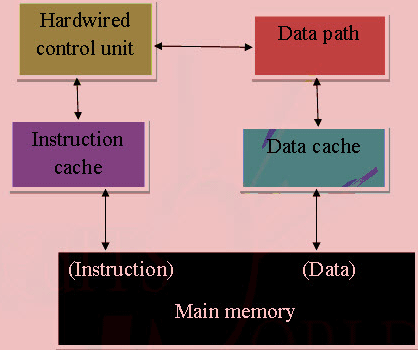
Functional units of 8086
8086 contains two independent functional units: a Bus Interface Unit (BIU) and an Execution Unit (EU).
Fig: Block Diagram of Intel 8086 Microprocessor (8086 Architecture)
Bus Interface Unit (BIU)
The segment registers, instruction pointer and 6-byte instruction queue are associated with the bus interface unit (BIU).
The BIU:
Handles transfer of data and addresses,
Fetches instruction codes, stores fetched instruction codes in first-in-first-out register set called a queue,
Reads data from memory and I/O devices,
Writes data to memory and I/O devices,
It relocates addresses of operands since it gets un-relocated operand addresses from EU. The EU tells the BIU from where to fetch instructions or where to read data.
It has the following functional parts:
Instruction Queue: When EU executes instructions, the BIU gets 6-bytes of the next instruction and stores them in the instruction queue and this process is known as instruction pre fetch. This process increases the speed of the processor.
Segment Registers: A segment register contains the addresses of instructions and data in memory which are used by the processor to access memory locations. It points to the starting address of a memory segment currently being used. There are 4 segment registers in 8086 as given below:
Code Segment Register (CS): Code segment of the memory holds instruction codes of a program.
Data Segment Register (DS): The data, variables and constants given in the program are held in the data segment of the memory.
Stack Segment Register (SS): Stack segment holds addresses and data of subroutines. It also holds the contents of registers and memory locations given in PUSH instruction.
Extra Segment Register (ES): Extra segment holds the destination addresses of some data of certain string instructions.
Instruction Pointer (IP): The instruction pointer in the 8086 microprocessor acts as a program counter. It indicates to the address of the next instruction to be executed.
Execution Unit (EU)
The EU receives opcode of an instruction from the queue, decodes it and then executes it. While Execution, unit decodes or executes an instruction, then the BIU fetches instruction codes from the memory and stores them in the queue.
The BIU and EU operate in parallel independently. This makes processing faster.
General purpose registers, stack pointer, base pointer and index registers, ALU, flag registers (FLAGS), instruction decoder and timing and control unit constitute execution unit (EU). Let's discuss them:
General Purpose Registers: There are four 16-bit general purpose registers: AX (Accumulator Register), BX (Base Register), CX (Counter) and DX. Each of these 16-bit registers are further subdivided into 8-bit registers as shown below:
16-bit registers8-bit high-order registers8-bit low-order registersAXAHALBXBHBLCXCHCLDXDHDL
Index Register: The following four registers are in the group of pointer and index registers:
Stack Pointer (SP)
Base Pointer (BP)
Source Index (SI)
Destination Index (DI)
ALU: It handles all arithmetic and logical operations. Such as addition, subtraction, multiplication, division, AND, OR, NOT operations.
Flag Register: It is a 16?bit register which exactly behaves like a flip-flop, means it changes states according to the result stored in the accumulator. It has 9 flags and they are divided into 2 groups i.e. conditional and control flags.
Conditional Flags: This flag represents the result of the last arithmetic or logical instruction executed. Conditional flags are:
Carry Flag
Auxiliary Flag
Parity Flag
Zero Flag
Sign Flag
Overflow Flag
Control Flags: It controls the operations of the execution unit. Control flags are:
Trap Flag
Interrupt Flag
Direction Flag
Interrupts
Interrupt is a process of creating a temporary halt during program execution and allows peripheral devices to access the microprocessor.
Microprocessor responds to these interrupts with an interrupt service routine (ISR), which is a short program or subroutine to instruct the microprocessor on how to handle the interrupt.
There are different types of interrupt in 8086:
Hardware Interrupts
Hardware interrupts are that type of interrupt which are caused by any peripheral device by sending a signal through a specified pin to the microprocessor.
The Intel 8086 has two hardware interrupt pins:
NMI (Non-Maskbale Interrupt)
INTR (Interrupt Request) Maskable Interrupt.
NMI: NMI is a single Non-Maskable Interrupt having higher priority than the maskable interrupt. Imovie 9 download mac.
It cannot be disabled (masked) by user using software.
It is used by the processor to handle emergency conditions. For example: It can be used to save program and data in case of power failure. An external electronic circuitry is used to detect power failure, and to send an interrupt signal to 8086 through NMI line.
INTR: The INTR is a maskable interrupt. It can be enabled/disabled using interrupt flag (IF). After receiving INTR from external device, the 8086 acknowledges through INTA signal.
It executes two consecutive interrupt acknowledge bus cycles.
Software Interrupt
A microprocessor can also be interrupted by internal abnormal conditions such as overflow; division by zero; etc. A programmer can also interrupt microprocessor by inserting INT instruction at the desired point in the program while debugging a program. Such an interrupt is called a software interrupt.
Addressing Modes Of 8086 Video Lectures
The interrupt caused by an internal abnormal conditions also came under the heading of software interrupt.
Example of software interrupts are:
TYPE 0 (division by zero)
TYPE 1 (single step execution for debugging a program)
TYPE 2 represents NMI (power failure condition)
TYPE 3 (break point interrupt)
TYPE 4 (overflow interrupt)
Interrupt pointer table for 8086
Fig: Interrupt pointer table for 8086
The 8086 can handle up to 256, hardware and software interrupts.
1KB memory acts as a table to contain interrupt vectors (or interrupt pointers), and it is called interrupt vector table or interrupt pointer table. The 256 interrupt pointers have been numbered from 0 to 255 (FF hex). The number assigned to an interrupt pointer is known as type of that interrupt. For example, Type 0, Type 1, Type 2,......Type 255 interrupt.
Addressing modes of 8086
The way for which an operand is specified for an instruction in the accumulator, in a general purpose register or in memory location, is called addressing mode.
The 8086 microprocessors have 8 addressing modes. Two addressing modes have been provided for instructions which operate on register or immediate data.
These two addressing modes are:
Register Addressing: In register addressing, the operand is placed in one of the 16-bit or 8-bit general purpose registers.
Example
MOV AX, CX
ADD AL, BL
ADD CX, DX
Immediate Addressing: In immediate addressing, the operand is specified in the instruction itself.
Example
MOV AL, 35H
MOV BX, 0301H
MOV (0401), 3598H
ADD AX, 4836H
The remaining 6 addressing modes specify the location of an operand which is placed in a memory.
These 6 addressing modes are:
Direct Addressing: In direct addressing mode, the operand?s offset is given in the instruction as an 8-bit or 16-bit displacement element.
Example

ADD AL, (0301)
The instruction adds the content of the offset address 0301 to AL. the operand is placed at the given offset (0301) within the data segment DS.
Register Indirect Addressing: The operand's offset is placed in any one of the registers BX, BP, SI or DI as specified in the instruction.
Example

MOV AX, (BX)
It moves the contents of memory locations addressed by the register BX to the register AX.
Based Addressing: The operand's offset is the sum of an 8-bit or 16-bit displacement and the contents of the base register BX or BP. BX is used as base register for data segment, and the BP is used as a base register for stack segment.
Effective address (Offset) = (BX + 8-bit or 16-bit displacement).
Example
MOV AL, (BX+05); an example of 8-bit displacement.
MOV AL, (BX + 1346H); example of 16-bit displacement.
Indexed Addressing: The offset of an operand is the sum of the content of an index register SI or DI and an 8-bit or 16-bit displacement.
Offset (Effective Address) = (SI or DI + 8-bit or 16-bit displacement)
Example
MOV AX, (SI + 05); 8-bit displacement.
MOV AX, (SI + 1528H); 16-bit displacement.
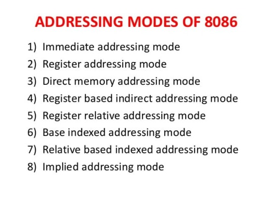
Based Indexed Addressing: The offset of operand is the sum of the content of a base register BX or BP and an index register SI or DI.
Effective Address (Offset) = (BX or BP) + (SI or DI)
Here, BX is used for a base register for data segment, and BP is used as a base register for stack segment.
Example
ADD AX, (BX + SI)
MOV CX, (BX + SI)
Based Indexed with Displacement: In this mode of addressing, the operand's offset is given by:
Effective Address (Offset) = (BX or BP) + (SI or DI) + 8-bit or 16-bit displacement
Example
MOV AX, (BX + SI + 05); 8-bit displacement
MOV AX, (BX + SI + 1235H); 16-bit displacement
Next TopicInstruction Set of 8086
Register Addressing
In register addressing the instruction will specify the name of the register which holds the data to be operated by the instruction.
Immediate Addressing
Addressing Modes Of 8086 With Examples
In immediate addressing mode an 8-bit or 16-bit data is specified as part of the instruction.
Direct Addressing
In direct addressing an unsigned 16-bit displacement of signed 8-bit displacement will be specified in the instruction.The displacement is the effective address(EA) or offset.The 20 bit physical address of memory is calculated by multiplying the content of DS register by 10H and adding to effective address.In case of 8-bit displacement, the effective address is obtained by sign extending the 8-bit displacement to 16-bit.
The segment base address (BA) is computed by multiplying the content of DS by 16(base 10)The memory address (MA) is computed by adding the effective address (EA) to the segment base address (BA)
Register Indirect Addressing
In register indirect adddressing the name of the register which holds the effective address(EA)will be specified in the instructionThis addressing mode allows data to be addressed at any memory location through an offset address held in any of the following registers: BP, BX, DI & SI.
Addressing Modes Of 8086 Pdf
This instruction moves a word from the address pointed by BX and BX + 1 in data segment into CL and CH respectively.
Based Addressing Mode
Addressing Modes Of 8086 In Hindi
In this addressing mode, the offset address of the operand is given by the sum of contents of the BX/BP registers and 8-bit/16-bit displacement.
Indexed Addressing Mode
In this addressing mode, the operands offset address is found by adding the contents of SI or DI register and 8-bit/16-bit displacements.
Addressing Modes Of 8086 Microprocessor
See Some Programs
0 notes
Text
Programming Language
If a programming language also written in programming language, how was the first programming language written?
Here’s a little amusing and true anecdote for you.
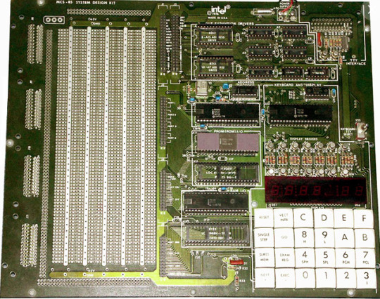
In the late 70’s, I was doing vac work with a research laboratory, and one of the tasks I was given was to build up a microprocessor board from components. Individual chips, resistors, capacitors, and a PC board. (The processor was an Intel 8085 - brand new at the time). It still surprises me all these decades later that as an untrained student I managed to get it to work - well, it did.
So, there I was, with a functioning microprocessor board. Initially, as input device it had a small hex keyboard (zero through nine, A through F, enter key, and I think it had a backspace - not sure about that though), and as output device it had a multiple-character LED segmented display capable of a single line of text. (Both input and output devices were subsequently replaced with better options, but that was the first configuration).
I managed to find the following image on the web. The one I built then was certainly similar to this.
he only interface ‘language’ was machine code. Not assembly - machine code. Bytes of machine language. For a short while it was fun coding tiny programs in hex and getting them to display stuff, but that wore off quickly. So, of course, this being the 70’s and not the early 60’s, the next goal was to make it understand a programming language - the one selected was interpreted Basic. We found a paper published by a Japanese guy (I think) which had a complete basic interpreter for the processor listed in machine code. I still remember with amusement that below the title of the paper was a tongue-in-cheek line which read “Copyleft, all wrongs reserved”. (Edit - someone found the original article. Li-Chen Wang published his “tiny basic” in 1976, and he was Chinese, not Japanese. Li-Chen Wang - Wikipedia )
I keyed in the entire program, and burnt it into whatever Eprom the system supported (probably something like 8 or 16 Kbyte). I must have got that right too, because from that point on it was possible to “talk” to the microprocessor in Basic.
So, one possible answer to your question : A first programming language can be brought into existence by implementing it in machine language, coding every byte manually, and burning it into an Eprom (or other programmable memory device).
0 notes
Text
300+ TOP MPMC LAB VIVA Questions and Answers
MPMC LAB VIVA Questions :-
1.What is a Microprocessor? It is a CPU fabricated on a single chip, program-controlled device, which fetches the instructions from memory, decodes and executes the instructions. 2. Define bit, byte and word. Bit is either 0 or 1. Byte is group of 8 bits. Word is group of 16 bits. 3.What are the different functional units in 8086? 2 units-Bus Interface Unit (BIU) and Execution unit (EU) 4. What is the function of BIU ? It is used to generate the 20-bit physical address and is responsible for performing all external bus operations. 5. What is the function of EU? Execution Unit receives program codes and data from BIU, executes these instructions and store the result. 6. What is the maximum size of segment in 8086 microprocessor? 64KB. 7. What is general purpose registers in 8086? There are 4 general purpose registers are there. AX-ACCUMULATOR BX- BASE CX- COUNT DX-DATA (Extended accumulator) 8. What are the functions of General purpose Registers? AX register as 16-bit accumulator, stores all arithmetic and logical operation's results. BX register is used as an offset address Storage. CX register is used as counter. Especially used in loop, shift, rotate instructions. DX register is used in port operations (IN and OUT) 9. What is special purpose registers in 8086? CS- CODE SEGMENT DS-DATA SEGMENT ES-EXTRA SEGMENT SS-STACK SEGMENT BP-BASE POINTER IP-INSTRUCTION POINTER SP- STACK POINTER SI-SOURCE INDEX DI-DESTINATION INDEX FLAG REGISTER 10. What are the functions of base Registers? CS stores program code, DS stores data ES sores extra data SS stores stack data. 11. Name the pin in 8086 microprocessor that is used for selecting mode of operation? 29th pin-MN/MX' If MN/MX'=0 then maximum mode is selected. MN/MX'=1 then minimum mode is selected. 12. What is Segment address in 8086? The part of the segment starting address stored in a segment register is called the segment address. 13. What are the flags in 8086? In 8086, 9 flags are there. Out of 9, 6 are conditional (status) flags and 3 control flags. Conditional (status) flags: Carry flag (CF), Parity flag (PF), Auxiliary carry flag (CF), Zero flag (ZF), Overflow flag (OF), and Sign flag(SF) Control flags: Trap flag (TF), Direction flag (DF), Interrupt flag (IF), 14. What is Tri-state logic? Three Logic Levels are used and they are High (logic 1), Low(logic 0), High impedance(Z) state. The high and low are normal logic levels & high impedance state is electrical open circuit conditions. 15. What is system bus? Group of address, data and control buses. Address bus: carry the Address to the memory to fetch either Instruction or Data. Data bus: carry the Data from the memory. Control bus: carry the Control signals like RD/WR, reset, ready etc. 16. What is the difference between Maskable interrupts and Non-Maskable interrupts? An interrupt that can be turned off by the programmer is known as Maskable interrupt. An interrupt which can be never be turned off (i.e. disabled) is known as Non-Maskable interrupt. 17. What are the different types of Addressing Modes? There are 12 different types of Addressing Modes. They are:- Immediate:- The Immediate data is a part of instruction. Direct:- A 16-bit memory address (offset) is directly specified in the instruction as a part of it. Register:- Data is stored in a register. Register Indirect:- The address of the memory location which contains data or operand is determined in an indirect way. Indexed:- offset of the operand is stored in one of the index registers. Register Relative:- The data is available at an effective address formed by adding an 8-bit or 16-bit displacement with the content of any one of the registers BX,BP,SI and DI in the default (either DS or ES) segment. Based Indexed:- The effective address of the data is formed, in this addressing mode,by adding content of a base register to the content of an index register. Relative Based Indexed:- The effective address is formed by adding an 8 or 16-bit displacement with the sum of contents of any one of the base registers and any one of the index registers, in the default segment. Intrasegment Direct Mode:- In this mode, the address to which the control is to bve transferred lies in the segment in which the control transfer instruction lies and appears directly in the instruction as an immediate displacement value. Intrasegment Indirect Mode:- In this mode, the displacement to which the control is to be transferred, is in the same segment in which the control transfer instruction lies, but it is passed to the instruction indirectly. Intersegment Direct:- In this mode, the address to which the control is to be transferred is in a different segment. Intersegment Indirect:- In this mode, the address to which the control is to be transferred lies in a different segment and it is passed to the instruction indirectly sequentially. 18. What is baud rate? The baud rate is the rate at which the serial data are transmitted. Units- symbols per second. 19. What is a port? The port is a buffered I/O, which is used to hold the data transmitted from the processor to I/O device or vice-versa. 20. What is 8255? It is PPI- Programmable Peripheral Interface. it is used to connect I/O devices to microprocessor and supports parallel communication. 21.What are Flag registers? 22.Write the flags of 8086? 23. What are the interrupts of 8086? 24. How clock signal is generated in 8086? What is the maximum internal clock frequency of 8086? 25. Write the special functions carried by the general purpose registers of 8086? 26.What is the need for Port? 27.What is a port? 28.What is processor cycle (Machine cycle)? 29.What is Instruction cycle? 30.What is fetch and execute cycle? 31. In how many ways computer soft wares are categorized? 32. Explain the two types of software? 33. What is an editor? 34. What is an OS and what are its functions? 35. What are the different types of assemblers used? 36. What is a linker? 37. What is a locator? 38. What is coprocessor? 39. What is a coprocessor trap? 40. What is a debugger? 41. In how many groups can the signals of 8085 be classified? 42. What is meant by the statement that 8085 is a 8 bit microprocessor? 43. What is the operating frequency of 8085? 44. What is the purpose of CLK signals of 8085? 45. What are the widths of data bus (DB) and address bus (AB) of 8085? 46. What is the distinguishing feature of DB and AB? 47. The address capability of 8085 is 64 KB.Explain? 48. Does 8085 have serial I/O control? 49. Mention the addressing modes of 8085? 50. What jobs ALU of 8085 can perform? 51. How many hardware interrupts 8085 supports? 52. How many I/O ports can 8085 access? 53. Why the lower byte address bus(A0-A7) and data bus (D0-D7) are multiplexed? 54. List the various registers of 8085? 55. Describe the accumulator register of 8085? 56. What are the temporary registers of 8085? 57. Describe the general purpose registers of 8085? 58. Which are sixteen bit registers of 8085? 59. Discuss PC and SP? 60. Describe the instruction register of 8085? 61. Describe the (status) flag register of 8085? 62. What is the function of ALE and how does it works? 63. Explain the functions of the two DMA signals HOLD and HLDA? 64. Discuss 3 states signals IO/M,S0,S1? 65. What happens when RESET IN(LOW) signal goes low? 66. Function of RESET OUT signal. 67. Indicate different machine cycles of 8085? 68. Name the special purpose registers? 69. Does ALU have any storage facility? 70. Explain XTHL,DAA,RC instructions. 71. What is the difference between JMP and CALL? 72. What happens when CALL instruction is executed? 73. Mention interrupts pins of 8085? 74. Explain maskable and non maskable interrupts? 75. Which is non maskable interrupt for 8085? 76. Do the interrupts of 8085 have priority? 77. What is meant by priority of interrupt? 78. Mention the types of interrupts that 8085 supports? 79. What is the software interrupts of 8085? 80. Explain the software instruction EI and DI? 81. Explain SIM and RIM instructions? 82. What is polling? 83. What is stack? 84. Why stack is used in program? 85. How the stack is initialized? 86. What the SP register does in a program? 87. Comment the size of stack? 88. What type of memory is the stack? 89. What are the software instructions related to stack operations? 90. What are the typical errors associated with using stack in a program? 91. What is a subroutine? 92. Why subroutine used in programs? 93. How subroutine can be called from the main program and how the program returns from the subroutine? 94. Byte wise what are the lengths of CALL and RET instructions? 95. Explain SPHL instruction? 96. Which are the different data transfer schemes? 97. Mention the types of programmed data transfer? 98. Explain DMA? 99. What is meant by address space? what is meant by address space partitioning? 100.Explain memory mapped I/O and I/O mapped I/O schemes? Read the full article
0 notes