#Placement in System Verilog
Explore tagged Tumblr posts
Visit Tumblr Blog
Explore Tumblr blogs with no restrictions, modern design and the best experience.
Last Seen Tumblr Blogs


Fun Fact
Tumblr’s website traffic is steadily declining.
Text
Paving the Path to VLSI Success: A Deep Dive into Learning Opportunities
The Rising Demand for VLSI Professionals
In today’s technology-driven world, the demand for skilled professionals in the field of Very-Large-Scale Integration (VLSI) continues to surge. VLSI technology forms the foundation of most modern electronic devices, from smartphones to satellites. As integrated circuits become more complex, the need for engineers who can design, test, and improve these systems grows. Engineering students and electronics graduates looking to future-proof their careers are increasingly drawn to VLSI as a specialization. Companies in India and around the world are on the lookout for talent equipped with practical VLSI skills, making this an attractive career path. Given this scenario, educational institutions and private training centers have stepped up to provide in-depth programs designed to meet industry needs. Aspiring engineers now have a variety of options to choose from when selecting the right program to build their foundation in VLSI technology.
Importance of Industry-Relevant Training in VLSI
While a formal degree in electronics or electrical engineering provides the basics, industry-relevant training in VLSI is critical for practical success. This is because VLSI is highly application-based, demanding a strong understanding of design tools, programming languages, and testing methodologies. Hands-on experience with CAD tools, simulation software, and real-time projects can make all the difference. As a result, the choice of a training institute becomes an important factor. Students looking to enter this domain often search for the top vlsi institutes in hyderabad, as Hyderabad is a major technology hub with several reputed centers offering quality training. These institutes focus on practical exposure, experienced faculty, and placement support, all of which are key to student success. With proper guidance and the right learning environment, students can gain the skills required to thrive in this competitive field.
Choosing the Right VLSI Course
Selecting the right VLSI course is essential for aligning one's career goals with market expectations. The ideal course not only covers theoretical knowledge but also emphasizes real-world application. Curriculum components typically include digital design, CMOS technology, Verilog/VHDL, ASIC design, and FPGA implementation. Additionally, courses offering modules on SystemVerilog, UVM, and embedded systems are becoming increasingly popular. When evaluating course offerings, many prospective students explore vlsi courses in hyderabad to find a comprehensive program that covers both front-end and back-end design processes. It is important for learners to also consider the duration, mode of delivery (online/offline), and availability of project work. A structured course with industry-certified trainers and access to advanced lab setups can provide a valuable edge in this field. This clarity helps learners not only gain knowledge but also build a strong portfolio that can appeal to future employers.
Placement Support and Career Opportunities
One of the biggest advantages of enrolling in a reputed VLSI training program is the access to placement support. Leading institutes often have tie-ups with semiconductor companies, startups, and multinational corporations looking for trained professionals. Career opportunities in VLSI are vast, ranging from physical design engineers to verification specialists and DFT engineers. With the growth of IoT, AI, and 5G technologies, VLSI engineers are finding exciting roles in hardware development teams across domains. Institutes that focus on industry connections, mock interviews, resume building, and internships significantly boost a student’s employability. Moreover, alumni networks and mentorship programs help learners stay updated on trends and job openings. A combination of technical skills and soft skills training can greatly improve the likelihood of landing a dream role. As the semiconductor industry continues to grow, so too does the demand for qualified, hands-on VLSI professionals.
Conclusion: Begin Your VLSI Journey with Confidence
Choosing the right institute and course is the first step toward a successful VLSI career. From understanding the fundamentals to mastering design and verification tools, a structured training program can be a game changer. Whether you're a fresh graduate or a working professional looking to switch domains, VLSI offers a dynamic and rewarding path. Hyderabad, as a tech hub, continues to provide ample opportunities for learning and growth in this field. Institutes that combine practical training, expert mentorship, and placement assistance can help bridge the gap between education and employment. If you're looking to start or elevate your career in this domain, takshila-vlsi.com is a reliable place to begin your journey.
0 notes
Text
Leading SystemVerilog and Verilog Training Institute in India
In today’s rapidly advancing semiconductor industry, knowledge of hardware description languages like Verilog and SystemVerilog is essential for anyone aiming to build a successful career in VLSI design and verification. Among the institutes offering quality training in this domain, Takshila Institute of VLSI Technologies has emerged as a top destination for professionals and students alike. Renowned for its comprehensive programs, it is widely recognized as one of the best System Verilog training institutes in Hyderabad and a trusted name for those seeking Verilog training institutes in Bangalore.
Takshila Institute of VLSI Technologies offers specialized training programs designed to provide in-depth understanding of Verilog and SystemVerilog, focusing on both RTL design and functional verification. The course begins with the fundamentals of digital design and gradually progresses to advanced topics such as constrained random verification, assertions, coverage analysis, and testbench architecture. This structured approach ensures that learners develop strong coding skills along with practical application in industry-level projects.
As one of the most sought-after SystemVerilog training institutes in Hyderabad, Takshila stands out for its hands-on teaching methodology. Students are trained using real-time projects and industry-standard EDA tools, enabling them to gain practical exposure that goes far beyond textbook learning. The institute's expert faculty, who bring years of industry experience, provide personalized guidance and mentorship throughout the course.
In addition, Takshila Institute is well known among learners seeking Verilog training institutes in Bangalore, thanks to its reputation for delivering high-quality online and hybrid learning options. Students from across the country enroll in its training programs due to the institute’s proven track record of successful placements, strong curriculum, and focus on career readiness.
What makes Takshila unique is its emphasis on both design and verification aspects. Whether you’re a beginner looking to learn Verilog from scratch or an experienced engineer aiming to master SystemVerilog for verification roles, the institute provides a pathway that aligns with individual career goals. Mock interviews, technical assessments, and resume preparation sessions are also part of the course to support students in their job search.
For those aspiring to become skilled VLSI engineers, Takshila Institute of VLSI Technologies offers the perfect blend of theoretical knowledge and practical experience. Recognized among the best SystemVerilog training institutes in Hyderabad and preferred by many searching for Verilog training institutes in Bangalore, Takshila is committed to empowering the next generation of semiconductor professionals with top-tier education and industry-aligned skills.
0 notes
Text
Takshila Institute of VLSI Technologies: Premier Verilog Training Institute in India
Verilog, a hardware description language (HDL), is fundamental in the design and development of digital systems, including microprocessors, FPGAs, and ASICs. Aspiring VLSI professionals often seek comprehensive training in Verilog to establish a strong foundation in digital design. Among the top choices for this specialized education is the Takshila Institute of VLSI Technologies, a renowned name in India offering exceptional Verilog training. Whether you're in Hyderabad or Bangalore, Takshila Institute stands out as a premier destination for mastering Verilog.
Takshila Institute’s Verilog training program is meticulously crafted to cater to students, fresh graduates, and working professionals. The course begins with the basics of digital design and progresses to advanced concepts, including combinational and sequential logic, testbenches, and synthesis. The curriculum emphasizes practical learning, allowing students to work on real-world design projects and understand how Verilog is used in creating functional digital systems.
One of the standout features of Takshila’s Verilog training is the hands-on experience it provides. Students gain expertise in writing, simulating, and debugging Verilog code using industry-standard tools such as Cadence and Synopsys. This practical exposure ensures learners can confidently apply their skills in professional environments. The program also includes modules on advanced design techniques, preparing students to tackle complex challenges in the VLSI domain.
The institute’s faculty comprises seasoned professionals with extensive experience in digital design and verification. Their personalized mentoring approach helps students grasp even the most challenging concepts with ease. Through interactive sessions and real-world examples, the faculty ensures that learners develop both theoretical knowledge and practical proficiency in Verilog.
Another advantage of choosing Takshila Institute is its strong placement support. The institute has established partnerships with leading semiconductor companies, enabling students to secure internships and full-time positions. Its dedicated placement team conducts mock interviews, resume-building workshops, and career counseling sessions, ensuring students are well-prepared for job opportunities in the VLSI sector.
Takshila Institute also caters to diverse learning needs by offering online verification training. This flexibility allows students from across India to access high-quality education without geographical constraints. Whether you are in Hyderabad, Bangalore, or any other part of the country, you can benefit from Takshila’s expert-led training programs.
In conclusion, the Takshila Institute of VLSI Technologies is a top-tier choice for those seeking Verilog training institutes in Bangalore. With its industry-aligned curriculum, experienced faculty, practical focus, and strong placement support, Takshila empowers students to excel in digital design and achieve their career goals in the VLSI industry.
0 notes
Text
FPGA System Design Training - VLSI Guru
In the evolving world of digital design, FPGA System Design Training has become a cornerstone for engineers aspiring to excel in hardware design and embedded systems. VLSI Guru’s comprehensive FPGA System Design course equips you with the skills to design, develop, and implement FPGA-based systems using the latest industry tools and methodologies.

What is FPGA System Design?
FPGA (Field-Programmable Gate Array) System Design involves programming configurable logic blocks to create customized hardware solutions. FPGAs are widely used in applications like embedded systems, signal processing, and high-performance computing due to their flexibility, scalability, and speed.
Why Choose VLSI Guru for FPGA System Design Training?
1. Industry-Focused Curriculum
VLSI Guru’s training covers all essential aspects of FPGA System Design, including:
Basics of FPGA architecture and design flow.
Programming using VHDL and Verilog.
Advanced concepts like timing analysis, IP integration, and system optimization.
Hands-on experience with industry tools like Xilinx Vivado and Intel Quartus.
2. Hands-On Learning
Our training emphasizes practical exposure, allowing you to work on real-world FPGA projects such as:
Designing digital circuits.
Implementing communication protocols.
Developing hardware acceleration modules.
3. Expert Mentorship
Learn from experienced trainers with extensive industry expertise, ensuring you gain insights into real-world FPGA system design challenges and solutions.
4. Placement Assistance
VLSI Guru provides job-oriented training along with resume building, interview preparation, and placement support to help you secure roles in top hardware and semiconductor companies.
What Will You Learn?
Fundamentals of FPGA architecture and HDL programming.
Design, simulation, and implementation using Verilog/VHDL.
Prototyping on FPGA development boards.
Debugging and optimization techniques for FPGA-based systems.
Who Should Enroll?
This course is ideal for:
Engineering graduates in electronics, electrical, or related fields.
Freshers and professionals seeking a career in FPGA System Design.
Embedded system developers looking to enhance their hardware design skills.
Why FPGA System Design is in Demand
FPGAs are the backbone of modern electronics, powering innovations in telecommunications, automotive, IoT, and artificial intelligence. Skilled FPGA engineers are in high demand to meet the growing need for customized hardware solutions.
Join VLSI Guru Today
Get ahead in the competitive semiconductor industry with VLSI Guru’s FPGA System Design Training. Our hands-on approach, expert guidance, and career support ensure you are ready to tackle the challenges of FPGA-based system design.
Contact us now to learn more and take the first step toward an exciting career in FPGA design
0 notes
Text
EP4CE15F23I7N
Unveiling the Power of the Intel EP4CE15F23I7N FPGA
Introduction:
The Intel EP4CE15F23I7N FPGA represents a pinnacle of programmable logic technology, offering unparalleled performance, versatility, and scalability. As a cornerstone in various electronic systems, this FPGA empowers engineers and developers to implement complex functionalities, accelerate time-to-market, and address diverse application requirements. In this comprehensive guide, we'll delve into the features, applications, and development process associated with the Intel EP4CE15F23I7N FPGA.
Understanding the Intel EP4CE15F23I7N FPGA:
At the heart of the Intel EP4CE15F23I7N lies a sophisticated architecture optimized for a myriad of tasks, ranging from embedded systems to high-performance computing.
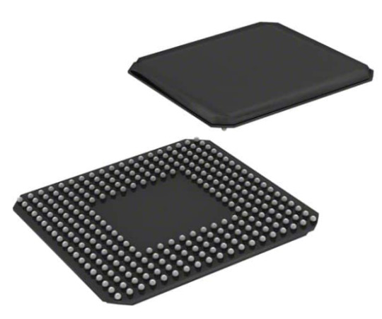
Architecture Overview:
The Intel EP4CE15F23I7N boasts a rich assortment of resources, including programmable logic elements, embedded memory blocks, high-speed transceivers, and dedicated input/output (I/O) pins. This flexible architecture enables designers to implement complex algorithms, signal processing chains, and control systems with precision and efficiency.
Key Features:
With features such as hardened processors, configurable DSP blocks, and advanced clocking resources, the EP4CE15F23I7N offers unparalleled flexibility and performance. These features are instrumental in meeting the demanding requirements of modern applications, including machine learning, image processing, and network acceleration.
Development Process:
To fully leverage the capabilities of the Intel EP4CE15F23I7N FPGA, developers must navigate through the stages of design, implementation, and validation with diligence and proficiency.
Design Entry:
Design entry can be accomplished using hardware description languages (HDL) such as Verilog or VHDL, or through graphical schematic entry tools. Intel's Quartus Prime Design Software provides a comprehensive platform for design entry, synthesis, and verification.
Synthesis and Optimization:
During synthesis, the HDL code is translated into a hardware netlist, which is then optimized for performance, area, and power consumption. Quartus Prime's synthesis and optimization tools enable designers to achieve the desired balance between these metrics while meeting stringent timing constraints.
Place and Route:
The place and route stage involves mapping the logical design onto physical FPGA resources and determining the routing of interconnections. Quartus Prime's advanced algorithms ensure optimal placement and routing, thereby maximizing performance and minimizing timing violations.
Testing and Validation:
Thorough testing and validation are imperative to ensure the reliability and functionality of the FPGA design.
Functional Simulation:
Functional simulation allows designers to verify the behavior of the FPGA design under different operating conditions and input stimuli. Comprehensive test benches and simulation tools facilitate rigorous testing and debugging.
Hardware Validation:
Once the design is synthesized, implemented, and verified through simulation, it is deployed onto a target FPGA device for hardware validation. Real-world testing validates the performance and functionality of the FPGA design in practical scenarios.
Conclusion:
The Intel EP4CE15F23I7N FPGA stands as a testament to innovation and engineering excellence, offering unmatched performance, versatility, and scalability. By mastering its architecture and development workflow, designers can unlock its full potential and realize groundbreaking solutions across diverse industries. Whether you're designing cutting-edge data processing systems, high-speed communication interfaces, or embedded control applications, the Intel EP4CE15F23I7N FPGA serves as a reliable and powerful enabler of technological advancement.
1 note
·
View note
Text
Best VLSI Training Institute (Courses) in Hyderabad | Maven Silicon
Join VLSI Course in Hyderabad at Maven Silicon. We are the best VLSI training institutes in Hyderabad, offer in VLSI Design, VLSI Course, System Verilog, UVM, Verilog & ASIC Verification courses. 100% placement assistance, Free Internship!
0 notes
Link
As the VLSI industry continues to evolve, the requirements for ASIC verification continue to expand to incorporate new ideas, which makes it essential for even professionals in the field to enroll in ASIC verification training to upgrade their knowledge from time to time. When it comes to UVM and ASIC verification training, Upgrade VLSI technologies ranks among the top 10 verification training institutes in Bangalore for a good number of reasons.
At Upgrade VLSI Technologies, we deliver advanced ASIC verification courses straight to your home. When you enroll for our ASIC verification and UVM course, you gain extensive knowledge of the different verification methodologies and Advanced Verilog for Verification. Other topics covered under the ASIC verification training includes:
RTL Design Training
System Verilog
UVM
Assertion Based Verification-SVA
Verification planning and management
Code and functional coverage
VIP coding style
Perl scripting language
At Upgrade VLSI Technologies, we offer a 5-month online verification training with six months internship. The course curriculum is designed to produce industry-ready professionals to fill up the gap between demand and supply in the industry.
Top Reasons Why Upgrade VLSI is Number One Choice for ASIC Verification Course#1 Upgrade VLSI Technologies Institutes is
low Cost Verification Training Institutes
If you are looking for an ASIC verification training institute in Bangalore that offers quality RTL Verification training at an affordable price P, Upgrade VLSI Technologies is the place to turn to for your training. Our prices are very competitive when compared to other VLSI institutes offering the same quality of lectures we offer.
#2
100%
Placement ASIC Verification Institute
If you are looking for an institution that guarantees you a 100% placement opportunity after your ASIC Verification training, Upgrade VLSI Technologies is the right institution for you. We offer ASIC verification online training with 100% placement support. Once you sign up with us, we provide you with the necessary assistance you need to become the best when it comes to UVM and ASIC verification. We continue to provide our trainees with the necessary placement support they require to excel as ASIC verification engineers. Over the years, Upgrade VLSI Technologies institute has remained the number one choice for students looking for an ASIC verification training institute with placement. Upgrade VLSI Technologies ranks among the best UVM training institutes when it comes to placement. Through a non-profit placement cell, we tap into the various placement opportunities in some of the top-tier semiconductor industries frequently for the sake of our trainees.
0 notes
Text
Mastering VLSI Design: A Comprehensive Training Path for Future Engineers
The Importance of VLSI Design in Modern Electronics
Very Large Scale Integration (VLSI) plays a pivotal role in the design and functioning of electronic devices that dominate our daily lives. From smartphones to automotive systems, VLSI is at the core of these innovations. As the semiconductor industry continues to evolve, the need for skilled professionals in this domain has become increasingly critical. VLSI design encompasses various stages including system-level design, RTL coding, functional verification, and physical implementation. Each stage requires a deep understanding of both theoretical concepts and practical skills. This has made structured training programs highly sought-after for aspirants wanting to enter the industry. Educational institutions and training centers across India are now focusing on offering specialized modules that help individuals develop end-to-end design capabilities. A well-structured course not only boosts technical knowledge but also enhances problem-solving abilities required in the dynamic field of chip design.
Why Functional Verification is a Crucial Skill
One of the most in-demand areas within the VLSI domain is functional verification. This process ensures that the chip behaves as intended before it goes into fabrication, reducing costly errors and time-to-market. Verification typically makes up more than 70% of a chip’s development timeline, emphasizing its importance. Learning verification techniques and tools is essential for engineers aiming to work in the semiconductor industry. Among the popular options for specialization is rtl verification training in hyderabad, where students are exposed to hands-on experience with industry-standard tools like UVM, SystemVerilog, and simulation environments. Such training not only imparts technical knowledge but also instills confidence in debugging and test-bench creation. The training covers key aspects like assertions, coverage, and test planning, equipping learners to tackle real-world verification challenges effectively.
Exploring the Role of SystemVerilog in Chip Development
SystemVerilog has emerged as the industry’s standard hardware description and verification language. It extends Verilog by adding advanced verification features like object-oriented programming, functional coverage, and constrained random verification. These enhancements make it easier to simulate and verify complex digital systems, making SystemVerilog expertise a valuable asset in the job market. Aspiring engineers looking for niche skill development often turn to system verilog training institutes in hyderabad for comprehensive education in this domain. These institutes provide in-depth courses that blend theoretical knowledge with practical implementation, ensuring that learners understand the nuances of verification methodologies. The learning curve may be steep initially, but structured training accelerates comprehension and builds long-term proficiency. Institutions with strong industry ties often provide opportunities to work on real-time projects and internships, enhancing the employability of students.
What to Look for in a Quality VLSI Training Institute
Choosing the right training institute can significantly influence an individual’s career path in VLSI design. Several factors should be considered including curriculum depth, experienced faculty, lab infrastructure, placement assistance, and industry collaborations. A good institute goes beyond textbooks, providing hands-on training on EDA tools, exposure to real-time case studies, and mock interviews to prepare students for industry demands. Interactive sessions, mentorship from industry experts, and regular assessments form the foundation of effective training. Additionally, flexible learning modes such as weekend batches and online classes cater to both students and working professionals. An ideal institute keeps pace with the latest industry trends and technological advancements to offer up-to-date content. Certification from a reputed institution adds credibility to the learner’s profile, boosting their chances of getting hired by top semiconductor companies.
Conclusion: Investing in a Future-Ready Career
The VLSI industry is a challenging yet rewarding field offering immense growth potential for skilled engineers. With continuous technological advancements, there is an increasing demand for professionals well-versed in both digital design and verification techniques. Investing in specialized training equips aspirants with the right tools and knowledge to succeed in this competitive space. Whether you're a recent graduate or an industry professional looking to upskill, choosing the right learning path is crucial. Structured courses, real-time project exposure, and industry-aligned curriculum are essential components of effective training. For those aspiring to carve a niche in VLSI, institutions like takshila-vlsi.com offer the ideal environment to grow and succeed.
0 notes
Text
The Growing Demand for VLSI Training and Career Opportunities
The Importance of VLSI in the Semiconductor Industry
The field of Very Large Scale Integration (VLSI) has seen exponential growth in recent years, driven by the rapid advancements in semiconductor technology. With the ever-increasing demand for high-performance chips used in smartphones, computers, automotive electronics, and artificial intelligence, VLSI has become a crucial aspect of modern electronics. The need for skilled professionals in this domain is rising, leading to the emergence of specialized training institutes that equip students with the necessary knowledge and hands-on experience. Engineers with expertise in VLSI design and verification are highly sought after by global technology firms, making this an attractive career path for aspiring electronics engineers.
Skills and Knowledge Required for a Career in VLSI
A successful career in VLSI requires a deep understanding of digital design, analog and mixed-signal design, system-on-chip (SoC) architecture, and verification methodologies. Programming skills in hardware description languages like VHDL and Verilog are essential, along with expertise in Electronic Design Automation (EDA) tools. The learning curve for VLSI professionals is steep, as it involves both theoretical concepts and practical applications. Many engineers and students opt for professional training programs to bridge the gap between academic knowledge and industry expectations. In particular, enrolling in one of the top 10 VLSI training institutes can provide a strong foundation and industry exposure, helping individuals stay ahead in this competitive field.
The Role of Training Institutes in Shaping VLSI Professionals
VLSI training institutes play a significant role in preparing students for real-world industry challenges. These institutes offer comprehensive courses covering fundamental to advanced topics, ensuring that learners gain practical expertise. Training programs often include hands-on projects, industry-relevant case studies, and internship opportunities that enhance problem-solving abilities. Many training centers collaborate with semiconductor companies, providing students with valuable networking opportunities and job placements. Among the many options available, VLSI institutes in Bangalore are particularly renowned for their high-quality education and strong industry connections. As Bangalore is a hub for semiconductor companies, students trained here have a higher chance of securing rewarding job opportunities.
Career Opportunities and Future Scope in VLSI
With the rapid expansion of the semiconductor industry, the demand for skilled VLSI engineers continues to grow. Companies specializing in chip design, manufacturing, and embedded systems actively seek trained professionals who can contribute to the development of cutting-edge technologies. Career opportunities in this field are diverse, ranging from digital and analog design to verification and testing. Additionally, with the emergence of AI, IoT, and 5G, the scope for VLSI professionals is expanding further. Salaries in this domain are highly competitive, and individuals with specialized training can secure lucrative positions in leading global technology firms. Those who continue upgrading their skills and staying updated with industry trends will find themselves at the forefront of technological advancements.
Choosing the Right VLSI Training Institute
Selecting the right training institute is a crucial step in building a successful career in VLSI. Factors such as faculty expertise, course curriculum, industry collaborations, hands-on training, and placement assistance should be carefully evaluated before making a decision. Institutes that offer mentorship, real-time project exposure, and certification programs can significantly enhance a student’s career prospects. One such institute that has gained recognition for providing quality VLSI training is Takshila VLSI.com. By enrolling in a reputed training institute, aspiring VLSI professionals can equip themselves with the necessary skills and knowledge to excel in the semiconductor industry.
0 notes
Text
How To Choose Frontend Vs. Backend? A guide for Freshers

#VLSI frontend and backend are nothing but two different domains in the field of VLSI. The classification is based on the different steps involved in a typical ASIC design flow. Following diagram shows a typical design flow for an ASIC or SOC.
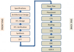
As it shows the design flow starts with a specification document which lists out the technical requirements needed in the chip design. It is followed by translating the specification to Architectural design. The architectural design involves designing the functional blocks and the communication protocol between them and translating them into actual modules that contain FSMs, combinational and sequential circuits etc. The architectural design is then modelled using a Hardware description language like Verilog/VHDL/System Verilog, which is the RTL design stage. The Functional Verification stage starts with a verification plan and a corresponding verification environment which describes and implements the method of proving the design correctness, using different Verification techniques. The design is refined until the HDL model is proved to be meeting the specifications.This stage is followed by Synthesis – a process of transforming the HDL design into a technology specific gate-level netlist, given all the specified constraints and optimization settings. DFT is a structural technique which facilitates a design to become testable after production. All the works till this stage are normally called as the Frontend of VLSI design and are executed by Frontend Engineers.
The next step in the ASIC Design flow is Placement and Routing which involves arranging approximate locations of a set of modules that need to be placed on a layout. Clock tree synthesis is a process which makes sure that the clock gets distributed evenly to all sequential elements in a design to fix the timing violations. This is followed by routing in which exact paths for the interconnection of standard cells and macros and I/O pins are determined.The file produced at the output of the layout is the GDSII (GDS2) file which is the file used by the foundry to fabricate the silicon. Gate level simulations and Static Timing Analysis (a method of validating the timing performance of a design by checking all possible paths for timing violations without having to simulate) are also done to make sure that the gate level design meets the timing requirements for correct design operations. All steps after logic synthesis are performed by Backend engineers and forms the Backend jobs.
Work of a Frontend Engineer
RTL Design/Coding
Synthesis
Functional Verification
DFT
Work of a Backend Engineer
Floor Planning
Placement
Clock Tree Synthesis
STA
Physical Verification
Which one has more career Opportunities?
With the advances being made in technologies like process geometries, feature size and product innovations on a daily basis, there is a constant need to design, develop and re-engineer integrated circuits (ICs). Since electronic products like mobile phones are being released with new features in shorter cycles, there is a healthy demand for qualified VLSI engineers to work on these products. Therefore, there is good scope for a career in the VLSI industry. The important point is that both the domains, front end and back end have their own advantages and have great career prospects. It is completely up to you which one to choose depending on your interest and confidence level, as both offer a great deal of learning and growth.
How to choose?
In order to become a front end engineer, one needs to have good knowledge of HDLs(Verilog/VHDL/SystemVerilog). It will be an added advantage if you have industry related protocol knowledge. So if you have ample digital fundamental knowledge, are fond of HDL coding, love debugging and want to have a sound understanding about the functionality of IC or chip you should definitely go for Front End. With the recent emergence of Artificial intelligence and its application towards VLSI opens up a huge scope for Front end engineers. In order to become a back end engineer, one needs to be well equipped with the concepts of digital electronics, CMOS and Analog Circuits, Scripting knowledge for automation, Hands on Tools for physical design, layout etc. If the above mentioned skills fascinates you then you can opt for Backend and there might be a chance to work in Foundry as well.
Challenges faced by a fresher to get into VLSI industry
Even though VLSI industry is a niche and has lots of career opportunities, on the flip side, industry is currently somewhat less reachable for fresh graduates, compared to other areas due to some particular reasons. Firstly, VLSI or chip design requires a deeper level of knowledge and skills than other electronics related fields .But our Universities are not catering 100% to the VLSI industry requirements. Secondly, VLSI chip design is expensive and requires access to high-cost, specialised electronic design automation (EDA) tools.
How can Chipedge help?
Chipedge offers various courses for fresh graduates both in frontend and backend domains, to choose from. The courses are well structured starting from building a strong foundation by emphasising on fundamental subjects like Digital, CMOS etc. Once the candidate becomes confident with the fundamental knowledge, we impart all the domain specific skills required for the VLSI industry, by giving hands on training on industry standard EDA tools (Synopsys).
1 note
·
View note
Text
System Verilog for Functional Verification in Bangalore – Inskill Courses
The demand for skilled professionals in functional verification is surging, driven by advancements in the semiconductor and VLSI industries. If you're looking to upskill in SystemVerilog-based functional verification, Inskill Courses in Bangalore offers the ideal platform to kickstart or advance your career.

Why SystemVerilog for Functional Verification?
SystemVerilog is a hardware description and verification language widely used for designing and verifying complex digital systems. It extends the capabilities of Verilog by adding object-oriented programming features, making it the go-to choice for functional verification.
Key benefits of mastering SystemVerilog include:
Comprehensive support for complex verification tasks.
Compatibility with advanced methodologies like UVM (Universal Verification Methodology).
Industry adoption by leading semiconductor companies.
About the Course
Inskill's SystemVerilog for Functional Verification course in Bangalore is designed to provide a solid foundation in SystemVerilog while addressing real-world verification challenges. Whether you're a fresher in VLSI or an experienced professional, this course caters to all levels of expertise.
What You’ll Learn:
Core concepts of SystemVerilog.
Advanced features like randomization, assertions, and coverage.
Building robust testbenches.
Applying UVM methodology for efficient verification.
Hands-On Learning
At Inskill, we believe in learning by doing. Our course emphasizes hands-on projects, enabling participants to apply theoretical knowledge to real-world scenarios. This practical exposure ensures you're job-ready from day one.
Why Choose Inskill in Bangalore?
Bangalore, the Silicon Valley of India, is a hub for technology and semiconductor industries. Inskill Courses is strategically located to connect you with opportunities in this thriving ecosystem. Here's why Inskill stands out:
Expert Trainers: Learn from industry veterans with years of experience in VLSI and functional verification.
Cutting-Edge Curriculum: Stay ahead with a syllabus tailored to current industry requirements.
Career Support: Get guidance for job placements and interviews.
Flexible Learning Options: Choose from classroom or online learning to suit your schedule.
Career Opportunities
After completing this course, you can pursue roles like:
Verification Engineer
ASIC Design Engineer
SystemVerilog Specialist
Functional Verification Expert
With the semiconductor industry booming, professionals skilled in SystemVerilog functional verification are highly sought after in Bangalore and beyond.
Enroll Now!
Take the first step towards a rewarding career in functional verification with Inskill Courses in Bangalore. Gain the knowledge, hands-on experience, and industry exposure needed to excel in VLSI verification.
1 note
·
View note
Text
Intel® Fpga Development Instruments Design
Our placement staff schedule placement drives and likewise conducts interview in several MNCs. Already, we've kept a average CMOS & FPGA Design Flow course charge to help college students coming from all sections of the society. Further, college students discover the CMOS & FPGA Design Flow coaching course duration flexible. CMOS & FPGA Design Flow course time is scheduled based on the coed's necessities.
The interconnect of an FPGA could be very totally different than that of a CPLD, but is somewhat just like that of a gate array ASIC. In Figure eleven, a hierarchy of interconnect sources can be seen. There are long traces which can be used to connect important CLBs which would possibly be bodily removed from each other on the chip with out inducing much delay. There are also brief traces that are used to connect individual CLBs that are positioned bodily close to each other.
They include just one performance in them and thru the lifetime of the chip, it could perform solely that perform. Its logic operate can't be changed to anything else as a result of its digital circuitry is made up of permanently connected gates and flip-flops on silicon. The difference in case of ASIC is that the resultant circuit is completely drawn into silicon whereas in FPGA the circuit is made by connecting numerous configurable blocks.
He has proficiency in SPICE, VHDL, Verilog, SystemVerilog, Xilinx ISE, Vivado, CoventorWare, COMSOL and LabVIEW programming. It may be “field” programmed to work as per the supposed design. It means it could work as a microprocessor or graphics card, and even as both directly. The designs running on FPGA’s are typically created utilizing hardware description languages such as VHDL and Verilog.
This two-day workshop in the space of FPGA design using Xilinx Vivado aims to enhance the intellectuals in direction of the design of digital circuits for real-time functions. Figure 8 FPGA Architecture Each FPGA vendor has its own FPGA architecture, but normally phrases they're all a variation of that proven in Figure 8. The structure consists of configurable logic blocks, configurable I/O blocks, and programmable interconnect. Also, there shall be clock circuitry for driving the clock signals to every logic block, and extra logic resources similar to ALUs, reminiscence, and decoders could additionally be obtainable. The two fundamental types of programmable components for an FPGA are Static RAM and anti-fuses. It is a tool that's created for a specific function or functionality.
There is commonly one or a quantity of switch matrices, like that in a CPLD, to attach these lengthy and brief strains collectively in particular ways. Programmable switches contained in the chip allow the connection of CLBs to interconnect lines and interconnect lines to each other and to the swap matrix. Three-state buffers are used to attach many CLBs to an extended line, creating a bus. Special lengthy lines, referred to as world clock traces, are specifically designed for low impedance and thus fast propagation times.
Our Electronic Design Automation ecosystem ensures that you've a whole design answer in designing, verifying, and integrating Intel® FPGAs into your methods. Find videos on the method to get began with Intel® Quartus® Prime and how to get the most effective performance on your Stratix 10 designs. This course trains you on the superior Design and Verification applied sciences and methodologies. One can simply enter into the VLSI trade with the talent units which may be gained by way of this coaching course. When the chips are put into production, it is essential to have some sort of burn-in check of your system that frequently tests your system over some lengthy period of time.
This information will allow us to route your request to the appropriate person. ITZIP conducts Personality Development periods together with Spoken English, Group Discussions, Mock Interviews, Presentation abilities to organize students Logic Fruit to face difficult interview situation with ease. ITZIP is the chief in providing placement to the students, as it has a devoted placement wing which caters to the wants of the students throughout placements.

This functionality supplies a simple methodology to confirm hardware implementation and accelerate simulations. No price training sessions are carried out on personality growth, spoken English, group dialogue, and mock interview to sharpen the presentation expertise. APTRON Gurgaon CMOS & FPGA Design Flow is all about sensible and follow; our classes embody concept and practical exposure for the students in studying. Join one of the best CMOS & FPGA Design Flow coaching in gurgaon supplied by APTRON Gurgaon to avail fast CMOS & FPGA Design Flow teaching, average course fee, and placement after Ab initio course.
The coaching happened remotely, nonetheless I really did not get the feel of distance hole. The trainer helped me to associated the course ideas with the IT industry that honed my artistic considering expertise. Attending CEH training at Multisoft Systems fulfills my objective utterly. Training starting from the basics of networking to the superior level of hacking expertise provides me nice publicity to the ethical hacking domain. Now, I’m confident sufficient to satisfy the security talent crisis of my group. The coaching was excellent and educated, filled with illustrations.
1 note
·
View note
Text
Best VLSI Training Institute in Pune | Maven Silicon
Join VLSI Course in Pune at Maven Silicon. We are the best VLSI training institute in Pune. We offer online and offline courses in VLSI Design, System Verilog, UVM, Verilog, ASIC Verification and such. 100% placement assistance, 24/7 Lab Access and support!
0 notes
Text
VLSI Technology: History, Usage and Design Process
VLSI Technology
Very large-scale integration is a process of embedding or integrating hundreds of thousands of transistors onto a singular silicon semiconductor microchip. VLSI technology's conception dates back to the late 1970s when advanced level processor (computer) microchips were also in their development stages. Two of the most common VLSI devices are the microprocessor and the microcontroller.
VLSI refers to an integrated circuit technology with numerous devices on a single chip. The remarkable growth of the electronics industry is primarily due to the advances in large-scale integration technologies. With the arrival of VLSI designs, the number of possibilities for ICs in control applications, telecommunications, high-performance computing, and consumer electronics as a whole continues to rise.
Presently, technologies like smartphones and cellular communications afford unprecedented portability, processing capabilities, and application access due to VLSI technology. The forecast for this trend indicates a rapid increase as demands continue to increase.
The Advantages of VLSI Technology
The following are the primary advantages of VLSI technology:
Reduced size for circuits
Increased cost-effectiveness for devices
Improved performance in terms of the operating speed of circuits
Requires less power than discrete components
Higher device reliability
Requires less space and promotes miniaturization
The Design Process of a VLSI IC
Overall, VLSI IC design incorporates two primary stages or parts:
1. Front-End Design: This includes digital design using a hardware description language, for example, Verilog, System Verilog, and VHDL. Furthermore, this stage encompasses design verification via simulation and other verification techniques. The entire process also incorporates designing, which starts with the gates and continues through to design for testability.
2. Back-End Design: This consists of checking the manufacturability of the chip. It involves placement, routing, clock tree synthesis, timing closure, LVS/DRC checks and a mask creation that can be delivered to the fabrication unit for manufacturing.
3. Fabrication: This consists of the processes involved in manufacturing a chip out of a piece of silicon.
The entire design process follows a step-by-step approach, and the following are the front-end design steps:
Problem Specification: This is a high-level interpretation of a system. We address the key parameters, such as design techniques, functionality, performance, fabrication technology, and physical dimensions. The final specifications include the power, functionality, speed, and size of the VLSI system.
Architecture Definition: This includes fundamental specifications such as floating-point units and which system to use, such as RISC or CISC and ALU's cache size.
Functional Design: This recognizes the vital functional units of a system and, thus, enables identification of each unit's physical and electrical specifications and interconnect requirements.
Logic Design: This step involves control flow, Boolean expressions, word width, and register allocation.
Circuit Design: This step performs the realization of the circuit in the form of a netlist. Since this is a software step, it utilizes simulation to check the outcome.
The following are the back-end design steps for hardware development:
Physical Design: In this step, we create the layout by converting the netlist into a geometrical depiction. This step also follows some preconceived static rules, such as the lambda rules, which afford precise details of the ratio, spacing between components, and size.
The following are the steps followed in a foundry for manufacturing a chip:
Wafer Processing: This step utilizes pure silicon melted in a pot at 1400º C. Then, a small seed comprising the required crystal orientation is injected into liquefied silicon and gradually pulled out, 1mm per minute. We manufacture the silicon crystal as a cylindrical ingot and cut it into discs or wafers before polishing and crystal orientation.
Lithography: This process (photolithography) includes masking with photo etching and a photographic mask. Next, we apply a photoresist film on the wafer. A photo aligner then aligns the wafer to a mask. Finally, we expose the wafer to ultraviolet light, thus highlighting the tracks through the mask.
Etching: Here, we selectively remove material from the surface of the wafer to produce patterns. With an etching mask to protect the essential parts of the material, we use additional plasma or chemicals to remove the remaining photoresist.
Ion Implantation: Here, we utilize a method to achieve a desired electrical characteristic in the semiconductor, i.e., a process of adding dopants. The process uses a beam of high-energy dopant ions to target precise areas of the wafer. The beam's energy level determines the depth of wafer penetration.
Metallization: In this step, we apply a thin layer of aluminum over the entire wafer.
Assembly and Packaging: Every one of the wafers contains hundreds of chips. Therefore, we use a diamond saw to cut the wafers into single chips. Afterward, they receive electrical testing, and we discard the failures. In contrast, those that pass receive a thorough visual inspection utilizing a microscope. Finally, we package the chips that pass the visual inspection as well as recheck them.
VLSI technology is ideally suited to the demands of today's electronic devices and systems. With the ever-increasing demand for miniaturization, portability, performance, reliability, and functionality, VLSI technology will continue to drive electronics advancement.
0 notes
Text
Track a Vehicle Using Telegram App and Live Location on Google Maps With ESP32
youtube
Remotely GPS Tracker with IoT and Telegram App Using ESP32 With Exact Location on Google Maps | GPS Based Vehicle Tracking Using ESP32 and Live Location on Google Maps With Telegram App | IOT. ****************************************************************** If You Want To Purchase the Full Project or Software Code Mail Us: [email protected] Title Name Along With You-Tube Video Link Project Changes also Made according to Student Requirements http://svsembedded.com/ è https://www.svskits.in/ M1: +91 9491535690 è M2: +91 7842358459 ****************************************************************** 1. Google Maps and Live Location Tracking, 2. How to track exact location of your family members by using Google maps, 3. Track Live Location With Google Maps - Google Maps Live Location, 4. How to Track Location of Your Family & Friends Using Google Maps, 5. TRACK YOUR VEHICLE USING GPS TELEGRAM, 6. GPS To Telegram Locator | GPS Vehicle Tracker , 7. HOW TO TRACK YOUR VEHICLE DEMO OF AS GPS TRACKER, 8. Best Way To Track Your Car Using Android Phone Or PC For FREE, 9. GPS tracker for Car and Bike , 10. How to Install HIDDEN GPS Tracker in any Car | Spy Car Tracker, 11. Installing High security GPS tracker on My New Car, 12. Mini GPS GF-07 Tracker for Vehicle Haw to Use setup the APP, 13. Telegram Bot on Android Device, 14. Android GPS Shield App for Arduino Projects, 15. Trace Mobile Number Current Location , 16. Trace Mobile Number Exact Location on Map | Find GPS, 17. How To Find a GPS Tracker on My Car, 18. EASY GPS TRACKER To Track Your CAR, 19. How To Track A Phone Number Location, 20. Car GPS Tracker - easy install video with Relay Disable - india car tracker | Tegnotech, 21. GPS and how it works, 22. How To Find a GPS Tracker on Your Vehicle, 23. How to Detect a GPS Tracker On My Car, 24. Remotely GPS tracker with raspberry pi4 via telegram app, 25. Gas Alert System with IoT and Telegram App Using ESP32, 26. How to install a Car GPS Tracker in your Car or Bike or Truck, 27. Never Lose Your Vehicle Again - Portable Real Time GPS Tracker Unboxing & Review, 28. How To Detect Hidden GPS Trackers On Any Vehicle, 29. How to Install a Car Tracker DIY Simple Easy Steps, 30. How to Book OLA Cab Step By Step in Hindi, 31. Track Any Mobile Number With Exact Location Using Your Device Itself 2017, 32. How to Use Google Maps, 33. New Device Lets You Track Your Vehicles Using Your Smartphone, 34. GPS Tracker For Car - Track your Teenage Driver, 35. Covert GPS Tracker Placement Tips, 36. How To: Track a Vehicle Using Your Mobile Phone, 37. how to track bike location without gps tracker system, 38. gps tracking system with android mobile, 39. TRACK YOUR CAR with CarLock - GPS ANTI-THEFT DEVICE, 40. Tracking vehicles using GPS or license plates, 41. Track Your Vehicles Anywhere in Nepal, 42. 5 Best Car GPS Tracker No Monthly Fee, 43. Track Your Car Using This Device, 44. Vehicle Tracking System Using GPS – GSM, 45. GPS + GSM Based Advanced Vehicle Tracking System Project, 46. Where is my car- Realtime GPS+GPRS Tracking of Vehicles using Arduino, 47. Car Tracking Device for Parents - Bouncie App Review, 48. GOOGLE TRACKER, Track your car for free using Google, 49. Spy GPS tracker GF-07 unboxing review, 50. GPS Based Vehicle Tracking and Theft Detection System, 51. GUI Based Error Correction In Data Communication Using MATLAB, 52. Ultrasonic Distance Meter Using Raspberry Pi 2, 53. IoT-Enabled Air Pollution Meter With Digital Dashboard On Smartphone, 54. USB Interface Using Python Software, 55. Line Frequency Meter Based On Reciprocal Counting, 56. Arduino Based Digital Capacitance Meter: An Interrupt Based Approach, 57. Duck Hunt Game Using Arduino And Python, 58. IoT Based Notification System Using Android App, 59. RGB Colour Detector Using TCS3200 Sensor Module, 60. Time For A Break, 61. Short-Range FM Radio Station, 62. Diode Tester Using MATLAB Based GUI, 63. Serial Interface Using Python Software, 64. Real-Time Face Recognition Using Python And OpenCV, 65. Memory Design Using Verilog, 66. Arduino based Windows PC volume remote control, 67. Make Your Own Remote-Controlled Robot, 68. Precision Stopwatch, 69. Electronic voting machine demo using MATLAB GUI, 70. Auto reversible DC motor with speed and rotation control, 71. Ultra-low-power sensor hub using nRF24L01 modules, 72. Electronic tone generator system, 73. PC-based oscilloscope using Arduino, 74. Image compression using discrete cosine transform technique, 75. Voting Machine Using AVR Microcontroller, 76. Countdown Timer, 77. Centre-of-Mass Extraction Using MATLAB, 78. Arduino Based Digital IC Tester Using MATLAB, 79. Fan Speed increasing Regulator Using PIC16F73, 80. Arduino-Based Smartphone Controlled Robot Car, 81. Demo Of 555 Timer-Based Astable Multivibrator Using MATLAB, 82. Computer Vision Based Quality Control Using Python,
0 notes
Link
Regardless of whether you happen to be a youthful engineer looking to go into the VLSI industry, or are aspiring to construct the most amazing profession, our UVM and ASIC verification training is unquestionably the training alternative that will work best for you. Our ASIC verification course trains budding engineers broadly on the foremost and the most trending verification strategies, in the end, helping them to join the VLSI verification industry as a portion of the foremost ASIC verification engineers. There are numerous reasons why we guarantee that our course is the one that will work best for you. A portion of those reasons are; We Lead All Other ASIC Verification Institutes As an aggregate that includes a few ASIC verification institutes with placement openings after you graduate, we are certainly the pioneer of the pack. We have online verification training that is offered in the entirety of our institutes including our ASIC verification training institutes in Bangalore, just as our ASIC verification training institutes in Hyderabad. This means you can join and experience our examinations from basically any piece of the world. Is there any comfort that outperforms this? Low Cost Training We are the foremost of all low cost verification training institutes you will ever find the world over. On the off chance that you analyze the measure of cash our understudies pay with the kind of training we offer, the instructors, materials, and most trending advances that we use in teaching, at that point you will comprehend that we offer much more incentive for the affordable value that we charge. This is among the key reasons why we are among the main 10 verification training institutes around. Dynamically more understudies from around the globe are seeing the worth we are offering and signing up for our ASIC verification course. The Best ASIC verification Course Around With the RTL verification training and System Verilog training that we have mixed into this course, we have had the option to beat all other System Verilog training institutes and Verilog training institutes. Different courses we have in the blend that causes this conceivable to include out VHDL training courses and our RTL design training. No institute offers a single course that combines such a wide assortment of vital training as we do. We do all these to guarantee that our understudies turn out the best the industry brings to the table when they graduate. Also, that is the motivation behind why we gladly offer 100% placement support after you graduate. We are certain that our understudies can contend with the best of them. The Best in UVM Verification Training We are the foremost among the best UVM training institutes in the event that you investigate the substance and setting of the UVM training that we provide for our understudies. UVM (Universal Verification Methodology) is an approach that defines the use of System Verilog to confirm complex designs. By joining us, you are acquiring the most standard UVM training from a standout among st other UVM training institutes in the entire world. UVM instructs engineers to compose reusable yet exceptionally exhaustive test conditions using a hearty procedure that offers a few propelled highlights. In the wake of going through our training, engineers become experts at applying UVM to exchange level verification, inclusion, age of constrained irregular tests, just as score boarding. Subjects that are educated by the foremost specialists of the industry in our training include UVM test stages, UVM utilities, UVM sequencers, UVM screens, UVM Registers, UVM class libraries, UVM production lines, UVM drivers, UVM scoreboards, just as the setup of UVM tests. We Have the Best UVM Training Institutes With the foremost UVM training institute in Bangalore which offers the best yet most affordable UVM training for professionals, you ought to be certain that we offer the best training that the industry has ever observed. We are the best UVM training institute with placement support for our understudies after the finishing of their training. This additionally makes us the best PERL training institute considering that we have the foremost specialists of the whole industry to instruct PERL to our understudies. Features and Features of the Course As the multifaceted nature of advanced systems develops, the strategies of verification are likewise becoming continuously progressively basic. Despite the fact that computerized designs could be confirmed by taking a glance at wave forms and conducting manual checks in the early beginnings, the present-day intricacy doesn't allow for such verification's any longer. Thusly, designers have been improving methods for automating the procedure. That is the reason we guarantee that we give our understudies the best conceivable training. The features of the highlights of our training include; Classes that are directed by the foremost specialists who are as of now working in the industry. All modules being cultivated together with hands-on undertakings. Assignments that include totally robotized verification flows. Research center help together with classwork practice presents just as the best course materials. The improvement of delicate abilities, UVM training which is work situated, together with 100% placement support. Incredible accentuation on UVM libraries and ideas, UVM test structuring just as utilitarian inclusion. Under taking on the most trending industry-acknowledged conventions. Taking everything into account, there are a few different explanations behind which our UVM and ASIC verification training is the alternative that will work best for you, particularly when you take all the novel highlights of the course into thought. Be that as it may, these recorded ones are sufficient to make you join us. That is without a doubt the best thing you can accomplish for your profession.
0 notes