
Don't wanna be here? Send us removal request.
Statistics
We looked inside some of the posts by vlsiguru24 and here's what we found interesting.
Average Info
Notes Per Post
1
Likes Per Post
1
Reblog Per Post
0
Reply Per Post
0
Time Between Posts
2 days
Number of Posts By Type
Text
9
Last Seen Tumblr Blogs


Fun Fact
If you dial 1-866-584-6757, you can leave an audio post for your followers.
Text
FPGA System Design Training in Bangalore - VLSI Gu
In the fast-paced semiconductor industry, expertise in FPGA design is highly sought after. If you’re looking to enhance your skills and become industry-ready, FPGA System Design Training in Bangalore by VLSI Guru is the perfect opportunity.

Why Choose FPGA System Design Training?
Field-Programmable Gate Arrays (FPGAs) are the backbone of modern digital systems. Mastering FPGA design allows engineers to create efficient, flexible, and high-performance solutions for various applications. The training covers essential topics like:
VHDL/Verilog programming
Simulation and synthesis
Timing analysis and debugging
FPGA architecture and implementation
Why VLSI Guru?
VLSI Guru is a leading institute in Bangalore offering industry-aligned FPGA System Design Training in Bangalore. With experienced trainers, state-of-the-art tools, and a practical curriculum, students gain hands-on experience and confidence in FPGA design.
Enroll today at VLSI Guru and take your first step toward an exciting career in FPGA design!
0 notes
Text
Physical Design Training in Bangalore - VLSI Guru
Bangalore, often referred to as the Silicon Valley of India, is a thriving hub for the semiconductor and electronics industries. For anyone aspiring to build a successful career in VLSI, gaining expertise in Physical Design Training in Bangalore is a must. At VLSI Guru, we offer industry-leading training programs designed to bridge the gap between academic concepts and practical industry requirements.

Why Choose VLSI Guru for Physical Design Training?
At VLSI Guru, our training is meticulously crafted to equip students with hands-on skills and in-depth knowledge of physical design concepts. Our course covers:
Floor Planning and Placement: Learn to optimize chip area and layout.
Clock Tree Synthesis (CTS): Gain expertise in minimizing skew and ensuring balanced clock distribution.
Routing and Timing Analysis: Master techniques to improve chip performance and resolve timing issues.
Design Rule Checking (DRC): Understand compliance with manufacturing constraints.
Our training program incorporates industry-standard tools like Cadence and Synopsys, ensuring students gain relevant and practical skills essential for the semiconductor industry.
Advantages of Physical Design Training in Bangalore
Being the semiconductor capital of India, Bangalore offers unparalleled opportunities to network with industry professionals and gain exposure to cutting-edge technologies. Companies specializing in ASIC and SOC design actively seek skilled physical design engineers. With VLSI Guru's training, you will gain a competitive edge to secure placements in top VLSI companies.
Key Features of VLSI Guru’s Training
Experienced Trainers: Learn from industry veterans with years of VLSI experience.
Practical Exposure: Work on live projects and real-world scenarios to solidify your understanding.
Comprehensive Curriculum: Covers topics such as standard cell libraries, power optimization, and chip tape-out methodologies.
Flexible Learning Options: Suitable for students, freshers, and working professionals.
Enroll Today and Excel in VLSI Design
VLSI Guru’s Physical Design Training in Bangalore is your pathway to a rewarding career. Whether you’re a fresher or a professional looking to upskill, our program will help you achieve your goals. With our focus on real-world applications, you’ll be job-ready and confident to tackle the challenges of the semiconductor industry.
Don’t wait! Join the best physical design training program in Bangalore and take the first step toward becoming a skilled Physical Design Engineer.
For more information, contact us or visit our training center in Bangalore today.
0 notes
Text
VLSI Design And Verification Course For Fresher - VLSI Guru
In the fast-paced world of technology, the VLSI (Very Large Scale Integration) domain stands as a cornerstone for innovations in electronics and semiconductor design. If you’re a fresher aiming to dive into this exciting field, the VLSI Design and Verification Course by VLSI Guru is your perfect launchpad.

Why Choose VLSI as a Career Path?
The demand for skilled professionals in VLSI design and verification is skyrocketing, with industries relying on advanced ASIC (Application-Specific Integrated Circuits) and FPGA (Field-Programmable Gate Arrays) to power cutting-edge technologies. From smartphones to autonomous vehicles, the scope of VLSI is vast and evolving.
What Does the Course Offer?
The VLSI Design and Verification Course by VLSI Guru is tailored for freshers, focusing on:
HDL Languages: Master Verilog and VHDL for RTL coding.
SystemVerilog & UVM: Learn modern verification methodologies for building robust testbenches.
ASIC Design Flow: Gain insights into the complete chip design process.
FPGA Prototyping: Get hands-on experience with FPGA tools and workflows.
Debugging & Tools Expertise: Work with industry-standard tools like Cadence, Synopsys, and Mentor Graphics.
Why VLSI Guru?
VLSI Guru emphasizes practical learning through real-world projects and labs. Freshers are trained to handle challenges in semiconductor design and verification, bridging the gap between academia and industry.
Who Can Enroll?
The course is ideal for engineering graduates in ECE, EE, or CSE with a passion for chip design and a desire to work in leading semiconductor companies.
Start your journey in the semiconductor industry today with VLSI Guru's specialized training.
0 notes
Text
Custom And Analog Layout Training In Bangalore - VLSI Guru
The VLSI (Very Large Scale Integration) industry is booming, offering vast opportunities for skilled professionals in custom and analog layout design. As a tech hub, Bangalore is a prime destination for those looking to excel in this field. Among the top training institutes, VLSI Guru stands out for its comprehensive and industry-relevant custom and analog layout training in Bangalore.
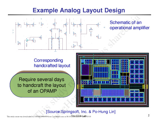
Why Choose Custom and Analog Layout Design?
Custom and analog layout design is a critical aspect of semiconductor design. It involves the intricate placement of transistors, resistors, capacitors, and interconnects to achieve high performance and precision in electronic circuits. Analog layout design focuses on ensuring signal integrity, power efficiency, and noise minimization, making it a sought-after skill in industries like consumer electronics, automotive, and telecommunications.
Professionals with expertise in custom and analog layout design are in high demand as they contribute to developing cutting-edge technologies such as IoT devices, AI processors, and advanced medical equipment.
Why Bangalore?
As India’s Silicon Valley, Bangalore hosts a thriving VLSI ecosystem, with leading semiconductor companies and startups establishing their presence here. This creates an ideal environment for aspiring VLSI professionals to acquire skills and secure opportunities. Whether you are a fresh graduate or an experienced engineer looking to upskill, Bangalore offers access to the best training facilities and industry connections.
Custom and Analog Layout Training at VLSI Guru
At VLSI Guru, we take pride in delivering a world-class custom and analog layout training program in Bangalore tailored to meet the current demands of the VLSI industry. Here's what sets us apart:
1. Comprehensive Curriculum
Our training program covers fundamental concepts and advanced techniques in custom and analog layout design. Topics include:
Basics of MOSFETs and CMOS Technology
Layout Design Rules (DRC and LVS)
Analog and Mixed-Signal Layout Techniques
Parasitic Extraction and Optimization
ESD (Electrostatic Discharge) Design Concepts
Tools like Cadence Virtuoso and Mentor Graphics
2. Hands-On Experience
At VLSI Guru, we believe that practical knowledge is key. Our training includes hands-on projects, lab sessions, and exposure to industry-standard EDA tools to ensure you gain real-world experience.
3. Experienced Faculty
Our instructors are industry veterans with years of experience in VLSI design and layout. Their insights help bridge the gap between academic concepts and practical applications.
4. Placement Assistance
We offer extensive support for career development, including resume building, mock interviews, and direct connections to top semiconductor companies in Bangalore.
5. Flexible Learning Options
Whether you prefer classroom sessions or online training, VLSI Guru provides flexible options to suit your schedule.
Who Can Benefit from This Training?
Fresh graduates in ECE, EE, or related fields aspiring for a career in VLSI design.
Professionals looking to switch or advance in the semiconductor industry.
Students interested in understanding custom and analog layout design for research or academic purposes.
Career Prospects in Custom and Analog Layout Design
After completing the training, you can explore roles such as:
Layout Design Engineer
Analog Design Engineer
CAD Engineer
Mixed-Signal Design Specialist
The demand for skilled layout designers is expected to grow with the advancements in AI, 5G, and IoT technologies.
Enroll Today with VLSI Guru!
If you’re passionate about building a career in custom and analog layout design, VLSI Guru in Bangalore is your ideal partner. With our state-of-the-art training and unwavering commitment to excellence, we empower you to succeed in the competitive VLSI industry.
Take the first step toward your dream career. Contact VLSI Guru today to learn more about our programs and enrollment details.
By targeting the custom and analog layout training in Bangalore keyword, this blog aims to help potential learners find the right platform to elevate their careers in VLSI design.
0 notes
Text
Custom And Analog Layout Training - VLSI Guru
In the ever-evolving world of semiconductor design, custom and analog layout plays a crucial role in developing high-performance, reliable, and efficient integrated circuits (ICs). If you are looking to specialize in custom layout and analog design, VLSI Guru in Bangalore offers one of the most comprehensive training programs to help you develop expertise in these highly sought-after fields.

Why Choose Custom and Analog Layout Training in Bangalore?
Bangalore, being the tech and semiconductor capital of India, is home to many leading VLSI companies, design houses, and startups. As a result, there is a significant demand for skilled professionals in custom and analog layout design. VLSI Guru offers custom and analog layout training that provides the foundation and practical skills needed to succeed in the competitive world of IC design.
This training program is ideal for engineers and students aiming to understand the intricacies of analog IC design, custom layout techniques, and their real-world applications. Whether you are a fresher or an experienced engineer, this program will take you through essential concepts and tools required for designing and laying out custom analog circuits.
What Will You Learn in Custom and Analog Layout Training at VLSI Guru?
At VLSI Guru, the custom and analog layout training program covers a wide array of topics to provide you with in-depth knowledge and hands-on experience in analog IC design and custom layout techniques. Here’s a look at the key modules you will explore:
1. Introduction to Analog Layout Design:
Gain an understanding of the fundamentals of analog design and its significance in the broader VLSI design flow.
Learn the principles of custom layout and how they apply to creating efficient and high-performing analog circuits.
2. Analog Circuit Design Fundamentals:
Study the basics of analog components such as transistors, resistors, capacitors, and how they interact in the design of complex circuits like amplifiers, oscillators, and filters.
Learn the different stages of analog design, including device sizing, biasing, and layout optimization.
3. Custom Layout Techniques:
Learn the art of custom layout design for analog circuits, focusing on key concepts like parasitics, matching, and layout-driven optimization.
Understand the importance of device matching and how to achieve optimal performance in analog circuits through effective layout techniques.
Work with tools like Cadence Virtuoso, which is widely used in the industry for custom and analog layout design.
4. Design Rules and Layout Verification:
Learn about the design rules (DRC) and layout verification techniques, which are essential for ensuring that your analog layouts meet manufacturing specifications.
Understand the importance of layout vs schematic (LVS) checks to ensure the layout matches the original circuit design.
5. Power, Area, and Performance (PPA) Optimization:
Gain an understanding of how to optimize analog layouts for power, area, and performance (PPA), which are key factors in VLSI design.
Explore techniques for minimizing power consumption and maximizing the performance of analog circuits while maintaining an efficient layout.
6. Analog Design Flow and Layout Automation:
Learn the end-to-end analog design flow, from schematic capture to layout implementation and verification.
Explore layout automation tools and scripts that help streamline the analog design process, reducing manual effort and ensuring design accuracy.
7. Hands-on Training and Real-World Projects:
The training includes practical sessions where you will work on real-world analog layout projects.
Apply the concepts you have learned to create analog ICs and optimize their layouts using industry-standard tools and workflows.
8. Advanced Topics in Analog Layout Design:
Study advanced topics such as deep submicron analog design, layout parasitics, and techniques for improving layout yield.
Learn how to tackle challenges in high-frequency analog designs, high-precision circuits, and mixed-signal layouts.
Why Choose VLSI Guru for Custom and Analog Layout Training in Bangalore?
At VLSI Guru, you will gain access to a highly specialized custom and analog layout training program taught by industry experts with years of experience in VLSI design and analog IC layout. Here's why VLSI Guru stands out as the preferred choice for training:
Expert Faculty: Learn from professionals who have extensive experience in custom layout and analog design, providing you with real-world insights and advanced techniques.
State-of-the-Art Tools: Get hands-on experience with the latest custom layout design tools like Cadence Virtuoso, Mentor Graphics, and others, widely used by top semiconductor companies.
Comprehensive Curriculum: The training program is designed to cover all aspects of custom and analog layout design, making it suitable for both beginners and advanced learners.
Industry-Relevant Projects: Work on live projects that simulate real-world VLSI design challenges, ensuring that you are job-ready after completing the training.
Career Opportunities: With the training provided at VLSI Guru, you will be well-equipped to pursue careers as analog layout engineers, IC designers, and VLSI engineers in leading semiconductor companies.
Career Opportunities After Custom and Analog Layout Training
Completing custom and analog layout training opens up a world of career opportunities in the VLSI design and semiconductor industries. Some of the key roles include:
Custom Layout Engineer
Analog IC Designer
VLSI Design Engineer
Physical Design Engineer
Analog Circuit Design Engineer
IC Layout Verification Engineer
With Bangalore being a major hub for semiconductor and VLSI design companies, professionals trained in custom layout and analog design are highly sought after.
Conclusion
In conclusion, Custom and Analog Layout Training at VLSI Guru in Bangalore is the ideal program for anyone looking to develop expertise in analog IC design and custom layout techniques. Whether you are just starting your career or looking to upskill, this training will provide you with the knowledge, tools, and hands-on experience needed to succeed in the competitive VLSI design industry.
Join VLSI Guru today and take your first step towards a successful career in custom and analog layout design!
Top of Form
Bottom of Form
0 notes
Text
DFT Training in Bangalore - VLSI Guru
In today’s rapidly evolving electronics industry, ensuring that complex integrated circuits (ICs) and systems function correctly is more critical than ever. This is where Design for Testability (DFT) comes into play. VLSI Guru, one of the leading training institutes in Bangalore, offers comprehensive DFT Training aimed at equipping engineers and students with the skills needed to excel in the world of semiconductor design and testing.

Why Choose DFT Training in Bangalore?
As the demand for VLSI design continues to grow, so does the need for skilled professionals who can ensure the reliability and performance of digital circuits. DFT is a critical aspect of the VLSI design process as it helps designers incorporate features that make it easier to test and validate integrated circuits (ICs). Engineers trained in DFT are equipped to tackle challenges in testing complex ICs, leading to high-quality products that meet industry standards.
Bangalore, the hub of India's tech industry, is home to numerous semiconductor companies and design houses. This makes DFT training in Bangalore a strategic choice for anyone looking to pursue a career in VLSI design and IC testing.
What Will You Learn in DFT Training at VLSI Guru?
VLSI Guru's DFT Training program provides in-depth knowledge of the essential concepts and techniques used in design for testability. Whether you are a beginner or have some experience in VLSI design, this training will help you build a strong foundation and advanced skills in DFT.
1. Introduction to DFT Concepts:
Learn the basic principles of DFT and its importance in the VLSI design process.
Understand the challenges of IC testing and why testability is critical for ensuring circuit functionality.
2. DFT Techniques:
Scan Chain Insertion: Learn how to insert scan chains into digital circuits to make them easier to test.
Boundary Scan: Understand how boundary scan methods allow for testing at the pins of ICs.
Built-In Self-Test (BIST): Study how BIST methodologies enable circuits to test themselves during operation.
Memory Test: Gain knowledge about techniques for testing memory modules used in IC designs.
3. Tools and Languages for DFT:
Explore industry-standard tools for DFT, such as Cadence, Synopsys, and Mentor Graphics.
Learn TCL scripting and its applications in automating DFT processes.
4. DFT for Different ICs:
Understand how to apply DFT techniques to various types of ICs such as ASICs, FPGAs, and SOC designs.
Learn to optimize test coverage for different circuit types.
5. Test Pattern Generation and Fault Models:
Study test pattern generation methods to identify potential faults in digital circuits.
Learn about various fault models and how to apply them in designing for better testability.
6. DFT for Low Power Circuits:
Explore techniques for ensuring that low-power designs also meet testability requirements without compromising performance.
7. Real-World Projects:
Work on real-world projects and case studies to develop practical experience in applying DFT techniques to actual VLSI designs.
Why Choose VLSI Guru for DFT Training?
VLSI Guru stands out as one of the best training providers for DFT training in Bangalore for several reasons:
Expert Trainers: The program is taught by industry experts with years of experience in DFT and VLSI design, offering hands-on insights into the latest techniques and tools.
Comprehensive Curriculum: The curriculum covers everything from basic concepts to advanced DFT techniques, making it suitable for both beginners and experienced engineers.
Hands-on Experience: You’ll get to work on real-world projects, allowing you to apply DFT techniques in a practical setting.
Career Support: The training program prepares you for lucrative career opportunities in VLSI design, IC testing, and semiconductor industries, all of which are in high demand in Bangalore.
Career Opportunities After DFT Training
Completing the DFT Training at VLSI Guru opens up a wide range of career opportunities. DFT-trained professionals are in demand in companies involved in semiconductor design, IC testing, embedded systems, and electronic manufacturing. Some potential job roles include:
DFT Engineer
Test Engineer
VLSI Design Engineer
ASIC Design Engineer
Validation Engineer
SOC Design Engineer
With Bangalore being a hub for VLSI design companies, the demand for professionals skilled in DFT is rising steadily, offering numerous job opportunities for those who complete this training.
Conclusion
In conclusion, DFT Training is an essential step for anyone looking to build a career in VLSI design and IC testing. VLSI Guru’s DFT training in Bangalore provides the right blend of theoretical knowledge and practical experience, making it an ideal choice for engineers and students who want to enhance their skills in Design for Testability.
Join VLSI Guru’s DFT Training program today and take your career to new heights in the world of VLSI design and testability.
0 notes
Text
FPGA System Design Training - VLSI Guru
In the evolving world of digital design, FPGA System Design Training has become a cornerstone for engineers aspiring to excel in hardware design and embedded systems. VLSI Guru’s comprehensive FPGA System Design course equips you with the skills to design, develop, and implement FPGA-based systems using the latest industry tools and methodologies.

What is FPGA System Design?
FPGA (Field-Programmable Gate Array) System Design involves programming configurable logic blocks to create customized hardware solutions. FPGAs are widely used in applications like embedded systems, signal processing, and high-performance computing due to their flexibility, scalability, and speed.
Why Choose VLSI Guru for FPGA System Design Training?
1. Industry-Focused Curriculum
VLSI Guru’s training covers all essential aspects of FPGA System Design, including:
Basics of FPGA architecture and design flow.
Programming using VHDL and Verilog.
Advanced concepts like timing analysis, IP integration, and system optimization.
Hands-on experience with industry tools like Xilinx Vivado and Intel Quartus.
2. Hands-On Learning
Our training emphasizes practical exposure, allowing you to work on real-world FPGA projects such as:
Designing digital circuits.
Implementing communication protocols.
Developing hardware acceleration modules.
3. Expert Mentorship
Learn from experienced trainers with extensive industry expertise, ensuring you gain insights into real-world FPGA system design challenges and solutions.
4. Placement Assistance
VLSI Guru provides job-oriented training along with resume building, interview preparation, and placement support to help you secure roles in top hardware and semiconductor companies.
What Will You Learn?
Fundamentals of FPGA architecture and HDL programming.
Design, simulation, and implementation using Verilog/VHDL.
Prototyping on FPGA development boards.
Debugging and optimization techniques for FPGA-based systems.
Who Should Enroll?
This course is ideal for:
Engineering graduates in electronics, electrical, or related fields.
Freshers and professionals seeking a career in FPGA System Design.
Embedded system developers looking to enhance their hardware design skills.
Why FPGA System Design is in Demand
FPGAs are the backbone of modern electronics, powering innovations in telecommunications, automotive, IoT, and artificial intelligence. Skilled FPGA engineers are in high demand to meet the growing need for customized hardware solutions.
Join VLSI Guru Today
Get ahead in the competitive semiconductor industry with VLSI Guru’s FPGA System Design Training. Our hands-on approach, expert guidance, and career support ensure you are ready to tackle the challenges of FPGA-based system design.
Contact us now to learn more and take the first step toward an exciting career in FPGA design
0 notes
Text
Physical Design Training - VLSI Guru
In the dynamic world of semiconductor design, Physical Design Training plays a crucial role in preparing aspiring professionals for backend design processes. If you're looking to excel in this field, VLSI Guru’s Physical Design Training provides the perfect blend of theoretical knowledge and hands-on experience, making you industry-ready.

What is VLSI Physical Design?
VLSI Physical Design refers to the process of transforming a circuit’s design (RTL) into its physical layout (GDSII), ready for fabrication. This involves steps like floorplanning, placement, clock tree synthesis (CTS), routing, and static timing analysis (STA). Mastering these skills is essential for anyone aspiring to work in backend VLSI design.
Why Choose VLSI Guru for Physical Design Training?
1. Industry-Aligned Curriculum
VLSI Guru’s training program covers the complete RTL to GDSII flow, ensuring you gain proficiency in:
Floorplanning and placement.
Routing and clock tree synthesis (CTS).
Timing optimization using STA.
Design Rule Check (DRC) and Layout Versus Schematic (LVS).
2. Hands-On Learning
Learn by working on real-world Physical Design projects using industry-standard tools like Cadence and Synopsys. This practical approach helps you understand challenges and solutions in a real semiconductor environment.
3. Expert Trainers
Our trainers are experienced VLSI professionals with years of experience in backend design. They provide valuable industry insights and mentorship throughout the training.
4. Placement Assistance
VLSI Guru goes beyond training by offering job support, career guidance, and interview preparation, helping you secure opportunities in top semiconductor companies.
What You Will Learn
Fundamentals of Physical Design and its importance in chip manufacturing.
Step-by-step understanding of RTL to GDSII implementation.
Optimization techniques for power, performance, and area (PPA).
Troubleshooting and debugging in backend design flows.
Who Should Enroll?
This program is ideal for:
Fresh graduates in electronics, electrical, or related fields.
Professionals looking to switch to backend VLSI roles.
Anyone eager to gain expertise in VLSI Physical Design.
Why Physical Design Training is In-Demand
The semiconductor industry is growing exponentially, and the demand for skilled Physical Design engineers is higher than ever. With VLSI Guru’s specialized training, you’ll gain the expertise needed to stand out in this competitive field and unlock lucrative career opportunities.
Take the Next Step with VLSI Guru
Whether you’re a fresher or an experienced professional, VLSI Guru’s Physical Design Training is your gateway to a successful career in VLSI backend design.
Contact us today to learn more and get started on your journey to becoming a VLSI Physical Design expert
0 notes
Text
VLSI Design And Verification Course For Fresher - VLSI Guru
VLSI Guru offers a comprehensive VLSI Design and Verification course for freshers, providing the perfect platform to kickstart your career in the semiconductor industry. Designed for engineering graduates and beginners, this course focuses on equipping students with the skills and knowledge needed to excel in VLSI design, verification, and front-end/back-end processes.

Why Choose VLSI Guru?
Industry-Relevant Curriculum: Our course covers all major aspects of VLSI design and verification, including RTL design, functional verification, SystemVerilog, UVM, and advanced techniques used in the industry.
Hands-On Training: Learn through practical assignments and projects that simulate real-world challenges in VLSI design and verification.
Expert Trainers: Our instructors are seasoned professionals with extensive experience in the VLSI industry, offering valuable insights and mentorship.
Job Assistance: We provide placement support and career guidance to help freshers secure opportunities in top semiconductor companies.
Flexible Learning Options: Choose from online or offline classes to suit your learning preferences.
What Will You Learn?
Fundamentals of VLSI design and verification.
Basics of digital design, Verilog, and SystemVerilog.
Advanced concepts in UVM methodology.
Practical skills to work on VLSI projects.
Who Should Enroll?
Engineering graduates in electronics, electrical, or related fields.
Freshers aspiring to build a career in VLSI design and verification.
Beginners looking for an in-depth, industry-oriented VLSI course.
Take the first step toward a rewarding career in the semiconductor domain with VLSI Guru’s VLSI Design and Verification course for freshers.
1 note
·
View note