#Semiconductor Bonding Market Semiconductor Bonding Market Size Semiconductor Bonding Market Share Semiconductor Bonding Market Growth Semico
Text
Global Semiconductor Bonding Market

Semiconductor Bonding Market size is projected to reach USD 1,135.79 million by 2028 from an estimated USD 904.89 million in 2021, growing at a CAGR of 3.3% globally.
Semiconductors encompass atoms bonded collectively to shape a homogeneous shape. In the bonding model, the shape of the cloth is homogeneous and truly comparable throughout. Semiconductor bonding is used within the making of numerous incorporated circuits and fabrication devices. The increase in complexity of semiconductor IC designs, growth with inside the want for semiconductor ICs which can carry out a couple of capabilities is major drives the marketplace at some point of the forecast period. Semiconductor Bonding Equipment is used for an incorporated chip to function, it wishes to be linked to the package deal or immediately to the broadcast circuit. This entails twine bonding, die-bonding, and dicing. Also, it's far a back-give-up system of chip formation. Increased usage of IoT devices and automated automotive components push the growth of the semiconductor bonding market.
#Global Semiconductor Bonding Market Size#Global Semiconductor Bonding Market Share#Global Semiconductor Bonding Market Growth#Global Semiconductor Bonding Market Trend#Global Semiconductor Bonding Market segment#Global Semiconductor Bonding Market Opportunity#Global Semiconductor Bonding Market Analysis 2022
0 notes
Text
Semiconductor Bonding Market

Semiconductor Bonding Market size is projected to reach USD 1,135.79 million by 2028 from an estimated USD 904.89 million in 2021, growing at a CAGR of 3.3% globally.
Market Scope:
The global semiconductor bonding market is growing rapidly. Semiconductors are found in all types of electronic devices. Semiconductor technology holds the immense potential to transform industries such as healthcare, manufacturing, and aerospace & defense, offering various innovative electronic devices. Resultantly, the market is witnessing increased funding and support from public and private organizations. With the substantial investments from OEMs, venture capitalists, and government bodies, the market is projected to perceive exponential gains during the next few years.
The parts that have a transmittance between transmission lines (often metals) and non-conductors or insulators are known as semiconductors (such as ceramics). Semiconductors can be made of pure elements like silicon or molecules like gallium arsenide. Physics explains the presumptions, traits, and mathematical strategy that govern semiconductors. Charged particles in this electronegativity shell are the ones that interact with nearby atoms. Such bonds are referred to as covalent bonds. Most conductors have just one electron in their valence shell. In contrast, the outermost shell of semiconductors typically has four electrons. However, electrons may interact with the valence electrons of other particles if the number of electrons in neighboring atoms is the same. When this happens, atoms self-organize into crystalline formations.
#Semiconductor Bonding Market#Semiconductor Bonding Market Size#Semiconductor Bonding Market Share#Semiconductor Bonding Market Growth#Semiconductor Bonding Market Trend#Semiconductor Bonding Market Opportunity
0 notes
Text
What is Semiconductor Bonding Market?
Semiconductor Bonding Market size is projected to reach USD 1,099.50 million by 2028 from an estimated USD 875.98 million in 2021, growing at a CAGR of 3.3% globally.
Market Scope:
The global semiconductor bonding market is growing rapidly. Semiconductors are found in all types of electronic devices. Semiconductor technology holds the immense potential to transform industries such as healthcare, manufacturing, and aerospace & defense, offering various innovative electronic devices. Resultantly, the market is witnessing increased funding and support from public and private organizations. With the substantial investments from OEMs, venture capitalists, and government bodies, the market is projected to perceive exponential gains during the next few years.
IMR offers a comprehensive overview of the market through the analysis of key parameters such as revenue, price, competition, and promotions, as well as the study, synthesis, and summarization of data from different sources. It analyzes the leading industry drivers and shows numerous market components. The information offered is thorough, dependable, and the result of a comprehensive primary and secondary study. IMR market research reports offer a comprehensive global market as well as an in-depth strategic sourcing methodology and analysis based on qualitative and quantitative research to anticipate market growth.
Key Players Covered In Semiconductor Bonding Market Are:
· BE Semiconductor Industries N.V.(Netherland)
· ASM Pacific Technology Ltd.(Singapore)
· Kulicke & Soffa(Singapore)
· Panasonic(Japan)
· Fuji Corporation(Japan)
· Yamaha Motor Robotics Corporation Co.(Japan)
· SUSS MicroTech SE(Germany)
· Shiaura Mechatronics(Japan)
Market has segmented the global Semiconductor Bonding market on the basis of type, application, and region:
By Type:
· Die Bonder
· Wafer Bonder
· and Flip Chip Bonder
By Application:
· RF Devices
· MEMS and Sensors
· LED
· 3D NAND and CMOS Image Sensors
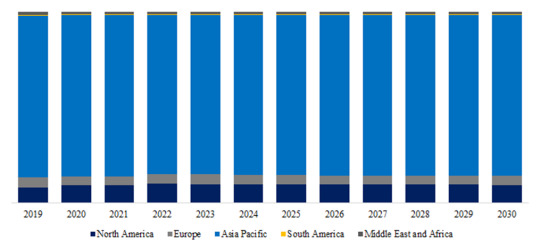
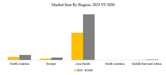
By Regional Outlook (Revenue, USD Billion, 2017 – 2028)
· North America (U.S., Canada, Mexico)
· Europe (Germany, U.K., France, Italy, Russia, Spain, Rest of Europe)
· Asia-Pacific (China, India, Japan, Southeast Asia, Rest of APAC)
· Middle East & Africa (GCC Countries, South Africa, Rest of MEA)
· South America (Brazil, Argentina, Rest of South America)
Get a Sample Copy of the Report@: https://introspectivemarketresearch.com/request/15917
Covid-19 Impact and Recovery Analysis on Industry:
The COVID-19 outbreak upset the balance of semiconductors supply and demand globally, resulting in a big gap in semiconductors' demand supply. Bonding materials are an important aspect of the semiconductor industry, required to establish systems for the stable supply of semiconductors. Bonding technology providers intend to contribute to the semiconductor industry by supplying sustainably around the world, even in states of emergency.
Share your Queries: https://introspectivemarketresearch.com/inquiry/15917
Semiconductor Bonding Market report covers the detailed analysis on current and upcoming market trends, company market shares, market projections, competitive benchmarking, competition mapping, and in-depth research of the most significant sustainability strategies and their impact on industry growth and competition. The research was conducted using a combination of primary and secondary data, as well as input from leading industry players.
How insights and forecasts from the reports could benefit you:
· To understand latest market dynamics and Demand & Supply situation
· Gauging timing and size of R&D activities
· To gear up or down production cycle to meet demand
· Ways to increase or decrease sales force activities
· Supporting & Adjust Investment/business decisions
· Benchmark and judge own competitiveness
· Assisting in allocating marketing investments
· Supporting company financial and cash flow planning
0 notes
Text
Aluminum Nitride Ceramics Market Regional Competitiveness, Revenue, Sales, and Market Evolution 2024 - 2031
The "Aluminum Nitride Ceramics Market" is a dynamic and rapidly evolving sector, with significant advancements and growth anticipated by 2031. Comprehensive market research reveals a detailed analysis of market size, share, and trends, providing valuable insights into its expansion. This report delves into segmentation and definition, offering a clear understanding of market components and drivers. Employing SWOT and PESTEL analyses, the study evaluates the market's strengths, weaknesses, opportunities, and threats, alongside political, economic, social, technological, environmental, and legal factors. Expert opinions and recent developments highlight the geographical distribution and forecast the market's trajectory, ensuring a robust foundation for strategic planning and investment.
What is the projected market size & growth rate of the Aluminum Nitride Ceramics Market?
Market Analysis and Insights :
Global Aluminum Nitride Ceramics Market
The aluminum nitride ceramics market is expected to witness market growth at a rate of 6.10% in the forecast period of 2021 to 2028. Data Bridge Market Research report on aluminum nitride ceramics market provides analysis and insights regarding the various factors expected to be prevalent throughout the forecast period while providing their impacts on the market’s growth. The rise in demand for the products from various end use industries is escalating the growth of aluminum nitride ceramics market.
Aluminum nitride, also called as nitride of aluminum with the chemical formula if AIN refers to covalently bonded metal that shows excellent thermal conductivity. The metal possesses hexagonal crystal structure and is generally manufactured by carbo-thermal reduction of aluminum oxide in the presence of gaseous nitrogen or ammonia.
The high usage of the metal in the production of semiconductors across the globe, acts as one of the major factors driving the growth of aluminum nitride ceramics market. The increase in demand for the product from several sectors owning to its most known properties including thermal conductivity, electric insulation, and mechanical strength and rise in use as a filler for power electronics and semiconductor packaging accelerate the market growth. The increase in the consumer inclination towards for aluminum nitride powder for electric vehicles over alumina due to its nine times higher thermal conductivity and surge in the utilization of the metal in evaporation boats, grinding media, crystal growing crucibles and thermocouple insulators further influence the market. Additionally, urbanization and digitization, growth of the semiconductor industry and increase in adoption due to minimum toxicity positively affect the aluminum nitride ceramics market. Furthermore, technological advancements in the metal and applications extend profitable opportunities to the market players in the forecast period of 2021 to 2028.
On the other hand, high cost associated with the aluminum nitride ceramics in comparison with regular alumina or zirconia is expected to obstruct the market growth. The volatility in raw material prices is projected to challenge the aluminum nitride ceramics market in the forecast period of 2021-2028.
This aluminum nitride ceramics market report provides details of new recent developments, trade regulations, import export analysis, production analysis, value chain optimization, market share, impact of domestic and localized market players, analyses opportunities in terms of emerging revenue pockets, changes in market regulations, strategic market growth analysis, market size, category market growths, application niches and dominance, product approvals, product launches, geographical expansions, technological innovations in the market. To gain more info on aluminum nitride ceramics market contact Data Bridge Market Research for an Analyst Brief, our team will help you take an informed market decision to achieve market growth.
Browse Detailed TOC, Tables and Figures with Charts which is spread across 350 Pages that provides exclusive data, information, vital statistics, trends, and competitive landscape details in this niche sector.
This research report is the result of an extensive primary and secondary research effort into the Aluminum Nitride Ceramics market. It provides a thorough overview of the market's current and future objectives, along with a competitive analysis of the industry, broken down by application, type and regional trends. It also provides a dashboard overview of the past and present performance of leading companies. A variety of methodologies and analyses are used in the research to ensure accurate and comprehensive information about the Aluminum Nitride Ceramics Market.
Get a Sample PDF of Report - https://www.databridgemarketresearch.com/request-a-sample/?dbmr=global-aluminum-nitride-ceramics-market
Which are the driving factors of the Aluminum Nitride Ceramics market?
The driving factors of the Aluminum Nitride Ceramics market include technological advancements that enhance product efficiency and user experience, increasing consumer demand driven by changing lifestyle preferences, and favorable government regulations and policies that support market growth. Additionally, rising investment in research and development and the expanding application scope of Aluminum Nitride Ceramics across various industries further propel market expansion.
Aluminum Nitride Ceramics Market - Competitive and Segmentation Analysis:
Global Aluminum Nitride Ceramics Market, By Grade (Technical Grade, Analytical Grade), Method (Carbothermal Reduction Method, Direct Nitridation Method, Nitridation Method), Form (Powder, Granules, Sheet), Application (Micro Electronics, Naval Radio, Power Electronics, Aeronautical System, Automotive, Emission Control, Others), Country (U.S., Canada, Mexico, Brazil, Argentina, Rest of South America, Germany, France, Italy, U.K., Belgium, Spain, Russia, Turkey, Netherlands, Switzerland, Rest of Europe, Japan, China, India, South Korea, Australia, Singapore, Malaysia, Thailand, Indonesia, Philippines, Rest of Asia-Pacific, U.A.E, Saudi Arabia, Egypt, South Africa, Israel, Rest of Middle East and Africa) Industry Trends and Forecast to 2031.
How do you determine the list of the key players included in the report?
With the aim of clearly revealing the competitive situation of the industry, we concretely analyze not only the leading enterprises that have a voice on a global scale, but also the regional small and medium-sized companies that play key roles and have plenty of potential growth.
Which are the top companies operating in the Aluminum Nitride Ceramics market?
The major players covered in the aluminum nitride ceramics market reports are 3M, CeramTec GmbH, CoorsTek Inc., FURUKAWA CO.,LTD, KYOCERA Corporation, MARUWA Co., Ltd., Nishimura & Asahi., Precision Ceramics, Surmet Corporation, Tokuyama Corporation., Toyal Toyo Aluminium KK, Liaoning Desunmet Special Ceramic Manufacture Co. Ltd, The American Ceramic Society, Thrutek Applied Materials, LEATEC Fine Ceramics Co,. Ltd., NIKKO CERAMICS, INC., Yokowo co., ltd., Ferrotec (USA) Corporation., NIPPON CARBIDE INDUSTRIES CO.,INC., KCC CORPORATION., and Heraeus Holding, among other domestic and global players.
Short Description About Aluminum Nitride Ceramics Market:
The Global Aluminum Nitride Ceramics market is anticipated to rise at a considerable rate during the forecast period, between 2024 and 2031. In 2023, the market is growing at a steady rate and with the rising adoption of strategies by key players, the market is expected to rise over the projected horizon.
North America, especially The United States, will still play an important role which can not be ignored. Any changes from United States might affect the development trend of Aluminum Nitride Ceramics. The market in North America is expected to grow considerably during the forecast period. The high adoption of advanced technology and the presence of large players in this region are likely to create ample growth opportunities for the market.
Europe also play important roles in global market, with a magnificent growth in CAGR During the Forecast period 2024-2031.
Aluminum Nitride Ceramics Market size is projected to reach Multimillion USD by 2031, In comparison to 2024, at unexpected CAGR during 2024-2031.
Despite the presence of intense competition, due to the global recovery trend is clear, investors are still optimistic about this area, and it will still be more new investments entering the field in the future.
This report focuses on the Aluminum Nitride Ceramics in global market, especially in North America, Europe and Asia-Pacific, South America, Middle East and Africa. This report categorizes the market based on manufacturers, regions, type and application.
Get a Sample Copy of the Aluminum Nitride Ceramics Report 2024
What are your main data sources?
Both Primary and Secondary data sources are being used while compiling the report. Primary sources include extensive interviews of key opinion leaders and industry experts (such as experienced front-line staff, directors, CEOs, and marketing executives), downstream distributors, as well as end-users. Secondary sources include the research of the annual and financial reports of the top companies, public files, new journals, etc. We also cooperate with some third-party databases.
Geographically, the detailed analysis of consumption, revenue, market share and growth rate, historical data and forecast (2024-2031) of the following regions are covered in Chapters
What are the key regions in the global Aluminum Nitride Ceramics market?
North America (United States, Canada and Mexico)
Europe (Germany, UK, France, Italy, Russia and Turkey etc.)
Asia-Pacific (China, Japan, Korea, India, Australia, Indonesia, Thailand, Philippines, Malaysia and Vietnam)
South America (Brazil, Argentina, Columbia etc.)
Middle East and Africa (Saudi Arabia, UAE, Egypt, Nigeria and South Africa)
This Aluminum Nitride Ceramics Market Research/Analysis Report Contains Answers to your following Questions
What are the global trends in the Aluminum Nitride Ceramics market?
Would the market witness an increase or decline in the demand in the coming years?
What is the estimated demand for different types of products in Aluminum Nitride Ceramics?
What are the upcoming industry applications and trends for Aluminum Nitride Ceramics market?
What Are Projections of Global Aluminum Nitride Ceramics Industry Considering Capacity, Production and Production Value? What Will Be the Estimation of Cost and Profit? What Will Be Market Share, Supply and Consumption? What about Import and Export?
Where will the strategic developments take the industry in the mid to long-term?
What are the factors contributing to the final price of Aluminum Nitride Ceramics?
What are the raw materials used for Aluminum Nitride Ceramics manufacturing?
How big is the opportunity for the Aluminum Nitride Ceramics market?
How will the increasing adoption of Aluminum Nitride Ceramics for mining impact the growth rate of the overall market?
How much is the global Aluminum Nitride Ceramics market worth? What was the value of the market In 2020?
Who are the major players operating in the Aluminum Nitride Ceramics market? Which companies are the front runners?
Which are the recent industry trends that can be implemented to generate additional revenue streams?
What Should Be Entry Strategies, Countermeasures to Economic Impact, and Marketing Channels for Aluminum Nitride Ceramics Industry?
Customization of the Report
Can I modify the scope of the report and customize it to suit my requirements? Yes. Customized requirements of multi-dimensional, deep-level and high-quality can help our customers precisely grasp market opportunities, effortlessly confront market challenges, properly formulate market strategies and act promptly, thus to win them sufficient time and space for market competition.
Inquire more and share questions if any before the purchase on this report at - https://www.databridgemarketresearch.com/inquire-before-buying/?dbmr=global-aluminum-nitride-ceramics-market
Detailed TOC of Global Aluminum Nitride Ceramics Market Insights and Forecast to 2031
Introduction
Market Segmentation
Executive Summary
Premium Insights
Market Overview
Aluminum Nitride Ceramics Market By Type
Aluminum Nitride Ceramics Market By Function
Aluminum Nitride Ceramics Market By Material
Aluminum Nitride Ceramics Market By End User
Aluminum Nitride Ceramics Market By Region
Aluminum Nitride Ceramics Market: Company Landscape
SWOT Analysis
Company Profiles
Continued...
Purchase this report – https://www.databridgemarketresearch.com/checkout/buy/singleuser/global-aluminum-nitride-ceramics-market
Data Bridge Market Research:
Today's trends are a great way to predict future events!
Data Bridge Market Research is a market research and consulting company that stands out for its innovative and distinctive approach, as well as its unmatched resilience and integrated methods. We are dedicated to identifying the best market opportunities, and providing insightful information that will help your business thrive in the marketplace. Data Bridge offers tailored solutions to complex business challenges. This facilitates a smooth decision-making process. Data Bridge was founded in Pune in 2015. It is the product of deep wisdom and experience.
Contact Us:
Data Bridge Market Research
US: +1 614 591 3140
UK: +44 845 154 9652
APAC: +653 1251 975
Email:- [email protected]
Browse More Reports:
Global Popping Boba/Juice Balls Market – Industry Trends and Forecast to 2031
Global Infrared Ear Thermometers Market – Industry Trends and Forecast to 2029
Global Cell Banking Outsourcing Market - Industry Trends and Forecast to 2029
Global Aluminum Nitride Ceramics Market – Industry Trends and Forecast to 2028
Global Automotive Night Vision Systems Market – Industry Trends and Forecast to 2029
0 notes
Text
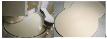
Polymer CMP Pads, Global Market Size Forecast, Top 10 Players Rank and Market Share
Polymer CMP Pads Market Summary
Chemical mechanical polishing/planarization (CMP) is a process that removes materials by a combination of chemical and mechanical (or abrasive) actions to achieve highly smooth and planar material surfaces. Chemical-mechanical polishing (CMP) is often associated with chemical-mechanical planarization which is a polishing process assisted by chemical reactions to remove surface materials. CMP is a standard manufacturing process practiced at the semiconductor industry to fabricate integrated circuits and memory disks. When the purpose is to remove surface materials, it is referred to as chemical-mechanical polishing. However, when the purpose is to flatten a surface, it is referred to as chemical-mechanical planarization. CMP is considered to be a tribochemical process because of the synergy between friction and corrosion. CMP Pad (Chemical Mechanical Polishing Pad) is a product which increases semiconductor integration by smoothening the semiconductor wafer surface through physical and chemical polishing processes.
Source: Secondary Sources and QYResearch, 2024
According to the new market research report “Global Polymer CMP Pads Market Report 2023-2030”, published by QYResearch, the global Polymer CMP Pads market size is projected to reach USD 1.38 billion by 2030, at a CAGR of 7.0% during the forecast period.
Figure. Global Polymer CMP Pads Market Size (US$ Million), 2019-2030
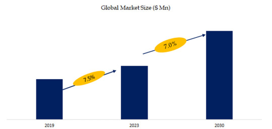
Above data is based on report from QYResearch: Global Polymer CMP Pads Market Report 2023-2030 (published in 2024). If you need the latest data, plaese contact QYResearch.
Figure. Global Polymer CMP Pads Top 10 Players Ranking and Market Share (Ranking is based on the revenue of 2023, continually updated)

Above data is based on report from QYResearch: Global Polymer CMP Pads Market Report 2023-2030 (published in 2024). If you need the latest data, plaese contact QYResearch.
According to QYResearch Top Players Research Center, the global key manufacturers of Polymer CMP Pads include DuPont, Entegris, etc. In 2023, the global top three players had a share approximately 82.0% in terms of revenue.
Figure. Polymer CMP Pads, Global Market Size, Split by Product Segment
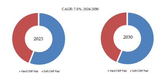
Based on or includes research from QYResearch: Global Polymer CMP Pads Market Report 2023-2030.
In terms of product type, Hard CMP Pad is the largest segment, hold a share of 55.9%,
Figure. Polymer CMP Pads, Global Market Size, Split by Application Segment
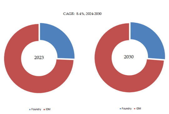
Based on or includes research from QYResearch: Global Polymer CMP Pads Market Report 2023-2030.
In terms of product application, IDM is the largest application, hold a share of 74.6%,
Figure. Polymer CMP Pads, Global Market Size, Split by Region
Based on or includes research from QYResearch: Global Polymer CMP Pads Market Report 2023-2030.
Market Drivers:
D1: The development of wafers has driven the development of its entire industrial chain, such as wafer shippers and carriers, wafer probe station, wafer bonding machine wafer grinder, electrostatic chucks, etc.
The development of the semiconductor industry has a continuous demand for wafer. Global achieved 9.28 billion USD from wafer, approximately 4% growth rate in the past few years.
The development of wafers will inevitably lead to the development of CMP polishing pads
D2: As a basic, leading and strategic pillar industry related to the overall national economy and social development, the semiconductor industry is strongly supported by various national policies. Among them, the huge localized replacement demand for core process materials in the semiconductor industry has become the general consensus of the market and the industry, showing a good situation of rapid growth. Benefited from the country's support for the semiconductor material industry and the rise of a number of companies in South Korea and China, the companies that started mass production in 2018 include South Korea's SKC (research and development and trial production before 2016) and Hubei Dinglong. These companies are expected to invest heavily in CMP polishing pads, and local companies will replace a large number of imported products.
D3: At present, advanced international chip manufacturers have used the 7-nanometer process technology, and the difficulty can be imagined. CMP enables chip manufacturers to continue to shrink circuit area and expand the performance of lithography tools. China and South Korea are countries with strong demand for CMP polishing pads. In the past, almost all CMP polishing pads in these countries depended on imports. After several years of development, the polishing pad technology of local manufacturers has the ability to replace overseas products. And local companies are expanding production on a large scale to replace imported products.
Restraint:
R1: CMP polishing pad is a key material in wafer polishing, and there is no alternative product. In addition, the market concentration of this industry is very high, and the suppliers are relatively stable. Furthermore, the product development and production costs are high and belong to a technology monopoly industry. So downstream customers have no bargaining power, but suppliers have strong bargaining power.
R2: The industry has a high technical threshold. New entrants must have a high level of technology, strong capital, broad sales channels, and the support of national policies to bring certain threats to leading companies. With the Japan-Korea trade war, the China–United States trade war continues to heat up. New entrants from China and South Korea expanded rapidly with the strong support of national policies, strengthened local brands to replace imported brands, and grabbed a certain market share.
Challenges:
C1: Trade deficits and disputes are the nodes that must be encountered for the rapid rise of national leading enterprises. During the trade war between Japan and South Korea, the Korean semiconductor industry was locked in the throat of fate because Japan restricted the export of key semiconductor materials. As a result, semiconductor materials have become the focus of attention from all walks of life. Korean domestic companies are facing great challenges. For example, FNS TECH Co., LTD, SKC is rapidly expanding production capacity. During the China–United States trade war, Hubei Dinglong Co., Ltd., a leading Chinese company, has increased its R&D and production of CMP polishing pads, expanded with the trend, and occupied a place.
C2: The raw material of Hard CMP Pad is mainly polyurethane, and the price fluctuation of raw materials has a certain impact on Hard CMP Pad. Considering the cost impact of all aspects, companies generally choose to purchase raw materials nearby.
C3: Under the influence of COVID-19, the global economy is declining. In the June report of the International Monetary Fund (IMF), almost all IMF member countries have lowered their predicted economic growth rates in 2020. In 2020, more than 95% of the country’s per capita income is expected to show negative growth, and the economic performance of export-oriented economies will be more severely affected.
About the Authors
Wei Qin
Lead Author
Semiconductor and Electronics
Email: [email protected]
About QYResearch
QYResearch founded in California, USA in 2007. It is a leading global market research and consulting company. With over 16 years’ experience and professional research team in various cities over the world QY Research focuses on management consulting, database and seminar services, IPO consulting, industry chain research and customized research to help our clients in providing non-linear revenue model and make them successful. We are globally recognized for our expansive portfolio of services, good corporate citizenship, and our strong commitment to sustainability. Up to now, we have cooperated with more than 60,000 clients across five continents. Let’s work closely with you and build a bold and better future.
QYResearch is a world-renowned large-scale consulting company. The industry covers various high-tech industry chain market segments, spanning the semiconductor industry chain (semiconductor equipment and parts, semiconductor materials, ICs, Foundry, packaging and testing, discrete devices, sensors, optoelectronic devices), photovoltaic industry chain (equipment, cells, modules, auxiliary material brackets, inverters, power station terminals), new energy automobile industry chain (batteries and materials, auto parts, batteries, motors, electronic control, automotive semiconductors, etc.), communication industry chain (communication system equipment, terminal equipment, electronic components, RF front-end, optical modules, 4G/5G/6G, broadband, IoT, digital economy, AI), advanced materials industry Chain (metal materials, polymer materials, ceramic materials, nano materials, etc.), machinery manufacturing industry chain (CNC machine tools, construction machinery, electrical machinery, 3C automation, industrial robots, lasers, industrial control, drones), food, beverages and pharmaceuticals, medical equipment, agriculture, etc.
0 notes
Text
Semiconductor Packaging Material Market - Worldwide Industry Share & Size & Growth, Gross Margin, Trend, Future Demand, Analysis By Top Leading Player And Forecast Till 2033
Future Outlook
The global market for semiconductor packaging materials was valued at USD 27.5 billion in 2022. By 2023, it is projected to reach USD 32 billion, growing at a CAGR of 7.2%. The market is forecast to surpass USD 71.5 billion by 2032, exhibiting a CAGR of 9.3% during the forecast period.
Miniaturization, demand for improved efficiency and thermal management in devices, and advanced packaging integration will drive future growth. The market faces challenges in the form of fluctuating raw material prices and declining PC sales. However, rising electronics demand from the automotive and industrial sectors is poised to create lucrative opportunities.
Take a Look at the Premium Report: https://dimensionmarketresearch.com/report/semiconductor-packaging-material-market/
Overview of the Semiconductor Packaging Materials Market
Semiconductor packaging provides interconnectivity, power delivery, heat dissipation, and physical protection to chips. It is an integral part of semiconductor manufacturing. Materials used for packaging include organic substrates, lead frames, bonding wires, encapsulation resins, ceramics, and die attach films among others.
With rising demand for consumer electronics and portable devices, manufacturers are developing new packaging technologies like Wafer-Level Packaging (WLP) and System-in-Package (SiP). This is expected to escalate the demand for innovative packaging materials.
Key Market Drivers
The proliferation of IoT and wearable technologies requiring miniaturized packages
Evolution of advanced System-in-Package architectures
Rising adoption of Flip Chip and Wafer Level packaging
Developments in Fan-Out panel-level packaging
Increased outsourcing to OSATs (Outsourced Semiconductor Assembly and Test providers)
Focus on enhancing thermal performance, efficiency, and reliability
Segmentation by Materials
The semiconductor packaging materials market is segmented into:
Organic Substrates
Bonding Wires
Leadframes
Encapsulation Resins
Ceramic Packages
Die Attach Materials
Others (lids, spacers)
Organic substrates dominate in terms of revenue contribution owing to their widespread usage and high cost. The die attach materials segment is slated for maximum growth fueled by the expanding use of flip chip interconnects.
Segmentation by Packaging Type
Based on packaging type, key segments include:
Flip Chip
Embedded Die
Fan-in WLP
Fan-out WLP
Flip chip packages account for the largest share driven by high I/O density requirements. However, Fan-Out WLP is expected to exhibit the highest CAGR owing to the rising adoption in mobile APs.
Segmentation by Technology
Different packaging technologies employ specific materials, hence driving demand patterns. Major technology segments are:
Grid Array Packages
Small Outline Packages
Flat No-leads Packages
Dual In-line Packages
Others like QFN, SOP, QFP etc.
Grid array packages contribute maximum market revenue. But declining use in PCs will restrain growth. In contrast, QFN packages are projected to drive robust demand owing to their rising adoption in automotive and IoT applications.
Regional Demand Dynamics
Asia Pacific drives the largest demand for semiconductor packaging materials because of high concentration of chip assembly units and OSAT providers, especially in China and Taiwan. North America and Europe are the other major markets. Developing economies are forecast to exhibit the fastest growth.
Competitive Environment
The market is highly consolidated with top companies occupying major shares.
Key players operating in the semiconductor packaging materials market include:
Samsung Electronics
TSMC Ltd.
Texas Instruments
Amkor Technology
Intel Corporation
Jiangsu Changjiang Electronics Tech Co.
IBM Corporation
Hitachi Chemical
Kyocera
Brewer Science
#semiconductormaterials#semiconductorpackaging#packagingmaterials#ICpackaging#semiconductorindustry#siliconpackaging#waferpackaging#SiP#systeminpackage#flipchip#fanoutWLP#embeddeddie#leadframes#substrates#bondwires#ceramicpackages#resinencapsulation#OSAT#semiconductorassembly#ICassembly#waferlevelpackaging#electronicsmanufacturing#mobileAPs#IoTdevices#wearabledevices#chippackaging#samsungsemiconductors#TSMC#TexasInstruments#AmkorTechnology
0 notes
Text
Electronic Adhesives: The $6.1 Billion Industry Force Powering Modern Electronics

The electronics industry is a rapidly growing sector that relies heavily on a variety of adhesives to ensure the functionality and reliability of electronic devices. These adhesives play a crucial role in bonding components, protecting sensitive circuits, and dissipating heat, making them indispensable for the production of modern electronics.
Market Size and Growth Projections
The global electronic adhesives market is expected to reach a staggering USD 6.1 billion by 2027, expanding at a compound annual growth rate (CAGR) of 6.1% from 2022 to 2027. This impressive growth is fueled by several factors, including:
Rising Demand for Electronic Devices: The increasing demand for smartphones, laptops, wearable devices, and other electronic gadgets is driving the need for high-performance adhesives that can meet the stringent requirements of the electronics industry.
Miniaturization of Electronic Components: As electronic components continue to shrink in size, the need for precision adhesives that can securely bond these tiny components is becoming increasingly important.
Advancements in Adhesive Technologies: Continuous advancements in adhesive technologies are leading to the development of new adhesives with improved properties, such as higher strength, heat resistance, and electrical insulation.
Types of Electronic Adhesives
A wide range of adhesives are utilized in the electronics industry, each with its unique properties and applications:
Epoxies: Epoxies are known for their exceptional strength, durability, and electrical insulation properties, making them ideal for bonding semiconductors, capacitors, and other electronic components.
Acrylics: Acrylics offer versatility and ease of application, making them suitable for bonding flexible printed circuits and other applications where flexibility is crucial.
Silicones: Silicones provide superior resistance to heat, chemicals, and vibration, making them excellent choices for sealing applications, protecting electronic components from environmental hazards.
Polyurethanes: Polyurethanes exhibit strong adhesion and remarkable bonding strength to a variety of substrates, making them suitable for bonding metal and plastic components in electronic devices.
Application Segments of Electronic Adhesives
The electronic adhesives market is segmented into various applications, each with its distinct growth drivers:
Semiconductor Manufacturing: The semiconductor industry is a major consumer of electronic adhesives, with adhesives used in wafer bonding, encapsulation, and device packaging.
Printed Circuit Board (PCB) Assembly: PCBs are the backbone of modern electronics, and adhesives play a critical role in bonding components, securing traces, and providing electrical insulation.
Consumer Electronics: Smartphones, laptops, tablets, and other consumer electronics devices rely heavily on adhesives for assembly, sealing, and heat dissipation.
Automotive Electronics: The increasing complexity of automotive electronics is driving the demand for high-performance adhesives that can withstand harsh automotive environments.
Medical Electronics: Medical devices require adhesives that meet stringent regulatory standards and offer biocompatibility with human tissues.
Geographical Landscape of the Electronic Adhesives Market
The global electronic adhesives market is dominated by Asia Pacific, primarily driven by the strong electronics manufacturing industry in China, South Korea, and Taiwan. North America and Europe also hold significant market shares due to their advanced technological expertise and established electronics manufacturing bases.
Key Players in the Electronic Adhesives Market
The electronic adhesives market is characterized by a competitive landscape, with several major players vying for market share:
Henkel AG & Co. KGaA
3M
H.B. Fuller Company
Dow Chemical Company
Huntsman Corporation
Eastman Chemical Company
Avery Dennison Corporation
Nitta Corporation
tesa SE
Würth Group
Download PDF Brochure :
The electronic adhesives market is poised for robust growth in the coming years, driven by the increasing demand for electronic devices, advancements in adhesive technologies, and the expansion of the electronics industry into new applications. As electronic devices become more complex and sophisticated, the role of electronic adhesives will become even more critical in ensuring the performance, reliability, and durability of these devices.
0 notes
Text
The Growth of Global Semiconductor Materials Market is segmented by Application (Fabrication (Process Chemicals, Photomasks, Electronic Gases, Photoresists Ancillaries, Sputtering Targets, and Silicon) and Packaging (Substrates, Lead Frames, Ceramic Packages, Bonding Wire, Encapsulation Resins (Liquid), and Die Attach Materials), by End-user Industry (Consumer Electronics, Telecommunication, Manufacturing, Automotive, and Energy and Utility), and by Geography (Taiwan, South Korea, China, Japan, North America, Europe, and Rest of the World).
0 notes
Text
Semiconductor Packaging Market Size Growth Of $60.44 Billion by 2030
According to a new report published by Allied Market Research, titled, “Semiconductor Packaging Market by Type, Packaging Material, Wafer Material, Technology, and Industry Vertical: Global Opportunity Analysis and Industry Forecast, 2021–2030” the global semiconductor packaging market size was valued at $27.10 billion in 2020 and is projected to reach $60.44 billion by 2030, registering a CAGR of 9.10% during the forecast period. Asia-Pacific is expected to be the leading contributor to the global market, followed by North America and Europe.
Semiconductor packaging is an advanced semiconductor packaging technology where the layers of components inside and integrated circuit (IC) are stacked together while the horizontal and vertical connections are made to keep them in place and work as a single device. Semiconductor packaging offers distinct advantages over other packaging technologies such as reduced power consumption, enhanced efficiency, better overall performance, and high frequency of operation.
Download Research Report Sample & TOC: Semiconductor Packaging Market Forecast, 2021–2030

Emerging technologies, such as artificial intelligence (AI) and quantum computing, require compound semiconductors to achieve full commercialization. The UK has a rich heritage of microprocessor design, with companies, such as ARM and Imagination Technologies, and new start-up companies designing AI processors, such as Bristol-based GraphCore, which are expected to create lucrative opportunities for the global semiconductor packaging market growth.
China is the largest country, in terms of revenue generation, in the global semiconductor packaging market share. The semiconductor packaging industry is well-established in China and Taiwan. In addition, rapid growth in sales of consumer electronic products supplements the market growth. Moreover, increase in defense expenditure and widespread use of semiconductors material in IT & telecommunication, consumer electronics, and automotive industries drive the growth of the semiconductor packaging market revenue. Increase in demand for high-speed and compact size electronic products boosts the adoption of flip chip technology in the electronic industry. Internet of Things (IoT) has been gaining popularity and serves as a key driver of the market.
Products used in IoT, such as sensors & actuators, analog & mixed-signal translators, and microcontrollers or embedded processors, require efficient and reliable packaging solutions, which can be done using flip chips, contributed the highest share in the global semiconductor packaging market. In comparison to customary wire-bond packaging, flip chip offers various benefits such as superior thermal & electrical performance, substrate flexibility for varying performance requirements, remarkable I/O capability, reduced form factors, and well-established process equipment expertise.
By region, the semiconductor packaging market trends have been analyzed across North America, Europe, Asia-Pacific, and LAMEA. The market analysis had identified that Asia-Pacific contributed maximum revenue in 2020 and is expected to grow at a faster rate as compared to other regions.
Inquiry Before Buying: Semiconductor Packaging Market
Covid 19 Impact Analysis
The impact of COVID-19 on the manufacturing industry has significantly affected the global economy. Electronic components, such as PCBs, LED chips and wafers, ICs, and other semiconductor devices, are mostly imported from China. Attributed to the shutdown of manufacturing units, the prices of semiconductor components have increased by 2-3%, owing to shortage of supplies.
The ongoing COVID-19 pandemic has abruptly re-shaped the global economy. Sudden decline in infrastructure development and installation projects is expected to hamper the semiconductor packaging market growth for automotive and other industrial verticals.
Key Findings Of The Study
In 2020, the flip chip segment accounted for maximum revenue and is projected to grow at a notable CAGR of 8.40% during the forecast period.
The consumer electronics segment accounted for more than 45% of the semiconductor packaging market share in 2020.
The fan-out WLP segment is expected to witness the highest growth rate during the forecast period.
UK was the major shareholder in the Europe semiconductor packaging market, accounting for approximately 35% share in 2020.
The key players profiled in the report include Amkor Technology (U.S.), ASE Group (Taiwan), ChipMOS Technologies, Inc. (Taiwan), Powertech Technology, Inc. (Taiwan), Intel Corporation (U.S.), Jiangsu Changjiang Electronics Technology Co., LTD (China), Samsung Electronics Co., Ltd. (South Korea), Taiwan Semiconductor Manufacturing Company (Taiwan), Texas Instruments (U.S.), and Fujitsu Limited (Japan). Market players have adopted various strategies, such as product launch, collaboration, product development, agreement, and expansion, to expand their foothold in the semiconductor packaging industry.
About Us:
Allied Market Research is a top provider of market intelligence that offers reports from leading technology publishers. Our in-depth market assessments in our research reports take into account significant technological advancements in the sector. In addition to other areas of expertise, AMR focuses on the analysis of high-tech systems and advanced production systems. We have a team of experts who compile thorough research reports and actively advise leading businesses to enhance their current procedures. Our experts have a wealth of knowledge on the topics they cover. Also, they use a variety of tools and techniques when gathering and analyzing data, including patented data sources.
Contact Us:
David Correa
1209 Orange Street
Corporation Trust Center
Wilmington
New Castle
Delaware 19801
USA Int'l: +1-503-894-6022
Toll Free: +1-800-792-5285
Fax: +1-800-792-5285
0 notes
Text
0 notes
Text
Wafer Bonding Equipment Market Size, Emerging Trends, Technological Advancements, and Business Strategies 2023-2029
The global Wafer Bonding Equipment market was valued at US$ 316.7 million in 2022 and is projected to reach US$ 461 million by 2029, at a CAGR of 5.5% during the forecast period. The influence of COVID-19 and the Russia-Ukraine War were considered while estimating market sizes.
Get Full Report @ https://semiconductorinsight.com/report/wafer-bonding-equipment-market/
Wafer bonding equipment is a type of semiconductor processing equipment used to bond two or more wafers together to form a single structure. This process is typically used to create complex semiconductor devices that require multiple layers or different materials.
Wafer bonding can be achieved through various techniques, including thermal compression bonding, adhesive bonding, and direct bonding. The choice of bonding technique depends on the materials being bonded, the required bonding strength, and the desired level of precision.
The equipment used for wafer bonding typically includes a bonding chamber or tool, which provides a controlled environment for the bonding process. The bonding surfaces of the wafers are carefully cleaned and prepared to ensure a strong and uniform bond. The wafers are then aligned and brought into contact with each other under controlled pressure and temperature conditions.
Wafer bonding equipment is commonly used in the manufacturing of advanced semiconductor devices such as micro-electro-mechanical systems (MEMS), power devices, and sensors. The bonding process enables the creation of highly integrated devices with multiple functionalities and improved performance characteristics.
This report aims to provide a comprehensive presentation of the global market for Wafer Bonding Equipment, with both quantitative and qualitative analysis, to help readers develop business/growth strategies, assess the market competitive situation, analyze their position in the current marketplace, and make informed business decisions regarding Wafer Bonding Equipment.
This report contains market size and forecasts of Wafer Bonding Equipment in global, including the following market information:
Global Wafer Bonding Equipment Market Revenue, 2018-2023, 2024-2029, ($ millions)
Global Wafer Bonding Equipment Market Sales, 2018-2023, 2024-2029, (Units)
Global top five Wafer Bonding Equipment companies in 2022 (%)
Global key players of wafer bonding equipment include EV Group, SUSS MicroTec, Tokyo Electron, etc. Asia-Pacific is the largest producer of wafer bonding equipment, holds a share over 60%, followed by Europe, and North America. In terms of product, fully automatic is the largest segment, with a share over 80%. And in terms of application, the largest segment is MEMS, with a share about 40%.
We surveyed the Wafer Bonding Equipment manufacturers, suppliers, distributors and industry experts on this industry, involving the sales, revenue, demand, price change, product type, recent development and plan, industry trends, drivers, challenges, obstacles, and potential risks.
Total Market by Segment:
Global Wafer Bonding Equipment Market, by Type, 2018-2023, 2024-2029 ($ Millions) & (Units)
Global Wafer Bonding Equipment Market Segment Percentages, by Type, 2022 (%)
Fully Automatic
Semi Automatic
Global Wafer Bonding Equipment Market, by Application, 2018-2023, 2024-2029 ($ Millions) & (Units)
Global Wafer Bonding Equipment Market Segment Percentages, by Application, 2022 (%)
MEMS
Advanced Packaging
CIS
Others
Global Wafer-Bonding Equipment Market, by Wafer Size, 2018-2023, 2024-2029 ($ Millions) & (Units)
Global Wafer-Bonding Equipment Market Segment Percentages, by Wafer Size, 2022 (%)
4 Inch
6 Inch
8 Inch
12 Inch
Others
Global Wafer-Bonding Equipment Market, by End-User, 2018-2023, 2024-2029 ($ Millions) & (Units)
Global Wafer-Bonding Equipment Market Segment Percentages, by End-User, 2022 (%)
Integrated Device Manufacturers (IDMs)
Foundries
Global Wafer-Bonding Equipment Market, By Region and Country, 2018-2023, 2024-2029 ($ Millions) & (Units)
Global Wafer-Bonding Equipment Market Segment Percentages, By Region and Country, 2022 (%)
North America
US
Canada
Mexico
Europe
Germany
France
U.K.
Italy
Russia
Nordic Countries
Benelux
Rest of Europe
Asia
China
Japan
South Korea
Southeast Asia
India
Rest of Asia
South America
Brazil
Argentina
Rest of South America
Middle East & Africa
Turkey
Israel
Saudi Arabia
UAE
Rest of Middle East & Africa
Competitor Analysis
The report also provides analysis of leading market participants including:
Key companies Wafer-Bonding Equipment revenues in global market, 2018-2023 (Estimated), ($ millions)
Key companies Wafer-Bonding Equipment revenues share in global market, 2022 (%)
Key companies Wafer-Bonding Equipment sales in global market, 2018-2023 (Estimated), (Units)
Key companies Wafer-Bonding Equipment sales share in global market, 2022 (%)
Further, the report presents profiles of competitors in the market, key players include:
EV Group
SUSS MicroTec
Tokyo Electron
Applied Microengineering
Nidec Machinetool
Ayumi Industry
Shanghai Micro Electronics
U-Precision Tech
Hutem
Canon
Bondtech
TAZMO
TOK
Kulicke & Soffa
Market Drivers:
Growing demand for advanced semiconductor devices: The increasing demand for advanced semiconductor devices such as MEMS, power devices, and sensors is driving the growth of the wafer bonding equipment market. Wafer bonding enables the creation of complex devices with multiple layers and improved performance characteristics, which are essential for a wide range of applications.
Technological advancements in wafer bonding techniques: The development of new wafer bonding techniques such as plasma activation bonding, anodic bonding, and hybrid bonding is driving the growth of the wafer bonding equipment market. These techniques offer higher bonding strength, improved precision, and lower processing temperatures, which are essential for the manufacturing of advanced semiconductor devices.
Growing demand for 3D ICs and TSVs: The increasing demand for 3D integrated circuits (ICs) and through-silicon vias (TSVs) is driving the growth of the wafer bonding equipment market. Wafer bonding is a key process in the manufacturing of 3D ICs and TSVs, which offer higher performance, reduced form factor, and lower power consumption.
Rising demand for consumer electronics: The growing demand for consumer electronics such as smartphones, tablets, and wearable devices is driving the growth of the wafer-bonding equipment market. Wafer bonding is a critical process in the manufacturing of these devices, which require complex semiconductor structures and high-performance components.
Increasing investment in semiconductor manufacturing: The increasing investment in semiconductor manufacturing by governments and private companies is driving the growth of the wafer bonding equipment market. This investment is aimed at increasing the production capacity and improving the efficiency of semiconductor manufacturing, which requires advanced wafer-bonding equipment.
Get Full Report @ https://semiconductorinsight.com/report/wafer-bonding-equipment-market/
0 notes
Text
Lead Frame Market 2023 Global Industry Size, Share, Business Growth, Revenue|SH Materials, Mitsui High-tec, Enomoto, Dynacraft Industries, etc
The lead frame market refers to the market for metal frames used in the assembly and packaging of semiconductor devices. Lead frames are thin metal structures that serve as the mechanical support for integrated circuits (ICs) and other semiconductor components. They provide electrical connections between the IC chip and the external circuitry.
Lead frames are typically made of alloys such as copper or copper alloys, and they are manufactured through a stamping process. The lead frame design consists of a grid-like structure with lead fingers that extend outward from the chip bonding area. These lead fingers provide connection points for wire bonding or other interconnect technologies.
Free Download Link:-https://www.marketinforeports.com/Market-Reports/Request-Sample/470550
The lead frame market is closely tied to the semiconductor industry as lead frames are essential components in the production of ICs. The increasing demand for electronic devices, such as smartphones, tablets, automotive electronics, and consumer electronics, has been driving the growth of the lead frame market. The rise of emerging technologies like the Internet of Things (IoT) and artificial intelligence (AI) has further boosted the demand for semiconductor devices, thus impacting the lead frame market positively.
The market is characterized by the presence of both global and regional manufacturers. Major players in the lead frame market include semiconductor packaging companies, integrated circuit manufacturers, and specialized lead frame manufacturers. These companies offer a wide range of lead frame solutions tailored to specific requirements, such as different package sizes, lead counts, and configurations.
The lead frame market has witnessed advancements and innovations to meet the evolving demands of the semiconductor industry. This includes the development of new lead frame materials with improved thermal conductivity and electrical performance. Additionally, the miniaturization trend in the semiconductor industry has led to the introduction of smaller and more intricate lead frame designs to accommodate higher chip densities.
With the emergence of advanced packaging technologies, such as flip-chip packaging and system-in-package (SiP), the role of lead frames has evolved. While traditional lead frames are still widely used, alternative packaging technologies may reduce the reliance on lead frames in certain applications.
In conclusion, the lead frame market plays a crucial role in the semiconductor industry by providing mechanical support and electrical connections for ICs and semiconductor components. With the increasing demand for electronic devices and advancements in semiconductor packaging technologies, the lead frame market is expected to continue growing. The market is driven by the need for miniaturization, higher chip densities, and improved performance, leading to ongoing innovations in lead frame design and materials.
0 notes
Text
Elemental Fluorine Market Regional Size and Share Forecast

Color Cosmetics
Fluorine is a highly reactive, pale yellow gas with the atomic number 9 and the symbol F on the periodic table. It is the most electronegative and reactive of all the elements, and is found naturally in the Earth's crust as fluoride minerals. Elemental fluorine is extremely toxic, corrosive, and can ignite spontaneously in the presence of organic materials, such as wood or paper. It has a wide range of industrial applications, including the production of uranium, fluorocarbons, and many other chemicals. Due to its high reactivity, fluorine is not typically found in its elemental form in nature, but rather is usually bonded to other elements, such as hydrogen or chlorine.
Color Cosmetics Market Overview
The elemental fluorine market is relatively small and specialized, as its extreme reactivity and toxicity make it difficult to handle and transport safely. The majority of fluorine production is used to create other chemicals and materials, such as hydrofluoric acid, uranium hexafluoride, and fluorocarbons. These products have a wide range of industrial and consumer applications, including refrigeration, air conditioning, and semiconductor manufacturing. The demand for elemental fluorine is driven by the growth of these industries, as well as ongoing research and development in the fields of chemistry and materials science. However, due to concerns about the environmental impact of fluorocarbons, there is increasing interest in developing alternative materials that do not require elemental fluorine in their production processes.
Color Cosmetics Market Growth
The market for elemental fluorine is expected to experience modest growth in the coming years, driven by the expanding demand for fluorine-based chemicals and materials in a variety of industries. The use of hydrofluoric acid, in particular, is expected to drive growth, as it is a key component in the production of a range of products, including refrigerants, aluminum, and petroleum. Additionally, the growing demand for fluoropolymers, which are used in a wide range of applications, including electronics, aerospace, and automotive industries, is expected to drive growth. However, the market for elemental fluorine is also subject to various challenges, including concerns about the environmental impact of fluorocarbons and the high cost of production, which may limit growth in the short term.
Color Cosmetics Market Trends
One of the key trends in the elemental fluorine market is the increasing demand for fluoropolymers, which are highly durable and resistant to chemicals, heat, and other forms of damage. These materials have a wide range of applications in industries such as electronics, aerospace, and automotive, and are expected to continue to drive growth in the market. Another trend is the development of alternative materials that do not require elemental fluorine, due to concerns about the environmental impact of fluorocarbons. This trend is likely to accelerate as governments around the world implement regulations aimed at reducing greenhouse gas emissions and other forms of pollution. Additionally, advances in technology and manufacturing processes are expected to drive down the cost of elemental fluorine production, making it more affordable for a wider range of applications.
0 notes
Text
Japan BJapan Market 2023 by Top Key Players, Types, Applications and Future Forecast to 2030
https://theprose.com/post/713860/europe-data-exfiltration-protection-market-2023-data-analysis-brief-reviewhttps://theprose.com/post/713861/europe-deep-uv-led-market-2023-projected-industry-growths-to-2029https://theprose.com/post/713862/usa-aircraft-steel-brakes-market-2023-new-study-report-2029https://theprose.com/post/713863/europe-colored-tattoo-inks-market-future-demand-market-analysis-2029https://theprose.com/post/713864/europe-water-based-pharmaceutical-ink-market-overview-demand-size-analysis-2029https://theprose.com/post/713865/europe-robotic-position-sensor-market-2023-new-comprehensive-study-by-key-playershttps://theprose.com/post/713866/europe-bonded-wheels-market-2029-new-research-reporthttps://theprose.com/post/713867/usa-aviation-electric-actuator-systems-market-leading-countries-landscape-analysis-applicationhttps://theprose.com/post/713868/europe-glider-aircraft-market-2023-regions-type-application-2029https://theprose.com/post/713869/usa-semiconductor-bonder-machine-market-2023-top-trends-segments-analysis-2029https://theprose.com/post/713871/europe-chopsticks-disinfection-machine-market-2023-development-growth-trends-2029https://theprose.com/post/713872/usa-precision-stainless-fittings-and-valves-market-2023-latest-trends-with-advancementhttps://theprose.com/post/713873/europe-skateboard-trucks-market-is-expected-to-grow-at-an-active-cagrhttps://theprose.com/post/713874/usa-computer-container-technology-market-size-2023-shares-growth-cost-structureshttps://theprose.com/post/713875/europe-polyvinylidene-chloride-coated-film-market-2023-growth-trends-size-share-2029https://theprose.com/post/713876/usa-weld-positioner-market-share-size-trends-growth-2023-to-2029https://theprose.com/post/713877/europe-fipronil-market-to-witness-astonishing-growthhttps://theprose.com/post/713878/europe-emergency-case-industry-statistics-market-analysis-2029https://theprose.com/post/713879/europe-auto-dialer-systems-market-2023-data-analysis-brief-reviewhttps://theprose.com/post/713880/europe-aircraft-maintenance-management-solutions-market-2023-projected-industry-growths-to-2029https://theprose.com/post/713881/usa-copper-oxide-nanomaterials-market-2023-new-study-report-2029https://theprose.com/post/713882/europe-electromagnetic-interference-emi-shielding-materials-market-future-demand-market-analysis-2029https://theprose.com/post/713883/europe-self-checkout-kiosk-market-overview-demand-size-analysis-2029https://theprose.com/post/713884/europe-welded-steel-conveyor-chain-market-2023-new-comprehensive-study-by-key-playershttps://theprose.com/post/713885/europe-portable-homogenizers-market-2029-new-research-reporthttps://theprose.com/post/713886/usa-liquid-nitrogen-generators-market-leading-countries-landscape-analysis-applicationhttps://theprose.com/post/713887/europe-water-infrastructure-construction-market-2023-regions-type-application-2029https://theprose.com/post/713888/usa-swing-gate-opener-market-2023-top-trends-segments-analysis-2029https://theprose.com/post/713890/europe-medical-aesthetics-training-market-2023-development-growth-trends-2029https://theprose.com/post/713891/usa-mechanical-spring-starter-market-2023-latest-trends-with-advancement
0 notes
Text
Semiconductor Bonding Market2022: SWOT Analysis by Players Continues Explosive Growth by 2028

Semiconductor Bonding Market size is projected to reach USD 1,135.79 million by 2028 from an estimated USD 904.89 million in 2021, growing at a CAGR of 3.3% globally.
Semiconductors encompass atoms bonded collectively to shape a homogeneous shape. In the bonding model, the shape of the cloth is homogeneous and truly comparable throughout. Semiconductor bonding is used within the making of numerous incorporated circuits and fabrication devices. The increase in complexity of semiconductor IC designs, growth with inside the want for semiconductor ICs which can carry out a couple of capabilities is major drives the marketplace at some point of the forecast period. Semiconductor Bonding Equipment is used for an incorporated chip to function, it wishes to be linked to the package deal or immediately to the broadcast circuit. This entails twine bonding, die-bonding, and dicing. Also, it's far a back-give-up system of chip formation. Increased usage of IoT devices and automated automotive components push the growth of the semiconductor bonding market.
Read More: -
The report Semiconductor Bonding Market report provides an in-depth analysis of the Semiconductor Bonding market, including a detailed description of market growth and size, value, and the key opportunities in the market, as well as an outline of the factors that are and will be driving the industry's growth, taking previous growth patterns into account. The global Semiconductor Bonding market report provides an in-depth analysis of the market state of Semiconductor Bonding manufacturers, including the latest facts and data, SWOT analysis, and expert views from around the world. The cost structure, market size, Semiconductor Bonding Sales, Gross Margin and Market Share, Price, Revenue, Size, Forecast, and Growth Rate are all calculated in the report. The income earned from the sale of This Study and technologies by various application industries is considered in the report.
1 note
·
View note
Text
Bonding Wire for Semiconductor, Global Market Size Forecast, Top 10 Players Rank and Market Share
Bonding Wire for Semiconductor Market Summary
Bonding wire is the core material for semiconductor packaging. It is a component that connects pins and silicon wafers and transmits electrical signals. It is an indispensable core material in semiconductor production.
According to the new market research report “Global Bonding Wire for Semiconductor Market Report 2023”, published by QYResearch, the global Bonding Wire for Semiconductor market size is projected to reach USD 4115.5 million by 2029, at a CAGR of 3.1% during the forecast period.

Figure. .Global Bonding Wire for Semiconductor Market Size (US$ Million), 2018 VS 2022 VS 2029

Snapshot from QYResearch Report: Global Bonding Wire for Semiconductor Market Report 2023.
Figure. Global Bonding Wire for Semiconductor Market Size (US$ Million), 2018-2029

Snapshot from QYResearch Report: Global Bonding Wire for Semiconductor Market Report 2023.
Market Drivers
1 Growth of electronic equipment
As the electronic equipment market continues to expand, such as the demand for smartphones, tablets, computers, etc., the demand for semiconductor bonding wires has also increased accordingly. The chips and integrated circuits in these devices often require semiconductor bonding wires to connect different components on the chip.
2 Growth of the automotive electronics market
Automotive electronics is another important semiconductor market. As the level of automotive electronics increases, including the application of Internet of Vehicles, autonomous driving technology, etc., the demand for semiconductor bonding wires is also increasing.
3 Development of the energy industry
With the development of renewable energy and electrical energy storage technology, the demand for efficient energy conversion and storage devices has increased, which has also put forward higher requirements for semiconductor bonding wires.
The global top 10 manufacturers includes TANAKA Precious Metals, Heraeus, MK Electron, Nippon Micrometal Corporation, AMETEK(Coining), Beijing Dabo, TATSUTA Group, Kangqiang Electronics, Yantai Zhaojin Kanfort, Yantai Yesdo Electronic Materials. In 2022, the global top 10 players had a share approximately 70.3% in terms of revenue.
Figure. Bonding Wire for Semiconductor, Global Top 10 Players’ Ranking and Market Share in 2022


Snapshot from QYResearch Report: Global Bonding Wire for Semiconductor Market Report 2023.
Based on the product form, Bonding Wire for Semiconductor is divided into Copper Wires, Palladium Coated Copper Wire, Thick Copper Wires, Copper Ribbons, Gold Wire, Silver Wires. Among them, Gold Wires hold the largest market with a share of 76.3% in terms of revenue in 2022.
Figure. Bonding Wire for Semiconductor, Global Market Size, Split by Type Segment 2018-2029

Snapshot from QYResearch Report: Global Bonding Wire for Semiconductor Market Report 2023.
Bonding Wire for Semiconductor is widely used in Discrete Device Packaging, IC Packaging, Others. Among them, IC Packaging holds the largest market with a sales share of 72.7% in 2022.
Figure. Bonding Wire for Semiconductor, Global Market Size, Split by Application Segment 2018-2029

Snapshot from QYResearch Report: Global Bonding Wire for Semiconductor Market Report 2023.
For regions, the top consumption regions are China, United States, Europe, Japan, South Korea, China Taiwan and Others. China is the larger producing region with a revenue share over 41.8% in 2022.
Figure. Bonding Wire for Semiconductor, Global Market Size, Split by Region 2018 VS 2022 VS 2029

Snapshot from QYResearch Report: Global Bonding Wire for Semiconductor Market Report 2023.
About The Authors
Li Ting –Intermediate Analyst
Email: [email protected]
Liting is an intermediate analyst, specializing in chemical industry, agriculture, scientific instrument, etc. Analyst Liting has 3 years of experience in the chemical industry and consumer goods industry, focusing on APIs, chemical intermediates, instrument, etc.
About QYResearch
QYResearch founded in California, USA in 2007.It is a leading China market research and consulting company. With over 16 years’ experience and professional research team in various cities over the world QY Research focuses on management consulting, database and seminar services, IPO consulting, industry chain research and customized research to help our clients in providing non-linear revenue model and make them successful. We are recognized for our expansive portfolio of services, good corporate citizenship, and our strong commitment to sustainability. Up to now, we have cooperated with more than 60,000 clients across five continents. Let’s work closely with you and build a bold and better future.
QYResearch is a world-renowned large-scale consulting company. The industry covers various high-tech industry chain market segments, spanning the semiconductor industry chain (semiconductor equipment and parts, semiconductor materials, ICs, Foundry, packaging and testing, discrete devices, sensors, optoelectronic devices), photovoltaic industry chain (equipment, cells, modules, auxiliary material brackets, inverters, power station terminals), new energy automobile industry chain (batteries and materials, auto parts, batteries, motors, electronic control, automotive semiconductors, etc.), communication industry chain (communication system equipment, terminal equipment, electronic components, RF front-end, optical modules, 4G/5G/6G, broadband, IoT, digital economy, AI), advanced materials industry chain (metal materials, polymer materials, ceramic materials, nano materials, etc.), machinery manufacturing industry chain (CNC machine tools, construction machinery, electrical machinery, 3c automation, industrial robots, lasers, industrial control, drones), food, beverages and pharmaceuticals, medical equipment, agriculture, etc.
0 notes
Last Seen Blogs

fllowzn
f l ⭕ w z n


aya-a3
Petite plume

kanatatass-blog
☆puka puka~☆

macleoding
hope is kinda the whole point