#Silicon Wafers Analysis
Explore tagged Tumblr posts
Visit Tumblr Blog
Explore Tumblr blogs with no restrictions, modern design and the best experience.
Last Seen Tumblr Blogs


Fun Fact
69% of Tumblr users are millennials.
Text
E-beam Wafer Inspection Industry Expands with Need for Nanometer-Level Defect Detection
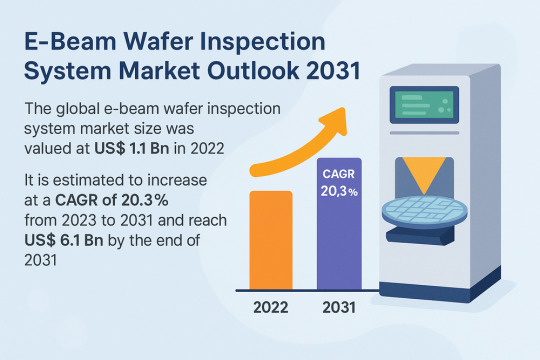
The global e-beam wafer inspection system market, valued at US$ 1.1 Bn in 2022, is projected to grow at a stellar CAGR of 20.3% from 2023 to 2031, reaching a market size of US$ 6.1 Bn by the end of 2031. As the semiconductor industry scales down to ever-smaller nodes and complex 3D architectures, electron beam (e-beam) wafer inspection systems are emerging as critical tools for defect detection and process optimization.
Market Overview: E-beam wafer inspection systems utilize high-energy electron beams to scan semiconductor wafers at nanoscale resolutions. These tools are essential in identifying particles, pattern anomalies, and line-width variations that are undetectable by traditional optical inspection systems. Their increasing application across memory and logic chip production lines highlights their importance in ensuring device reliability and performance.
Market Drivers & Trends
Miniaturization of Semiconductor Nodes: As manufacturers move toward 7nm, 5nm, and even smaller nodes, traditional optical inspection is insufficient. E-beam inspection offers the resolution and sensitivity required for these dimensions.
EUV Lithography Integration: EUV (Extreme Ultraviolet) lithography is now a standard in cutting-edge chip manufacturing. However, it introduces new stochastic defects and patterning challenges. E-beam inspection tools provide essential capabilities to detect these elusive defects early in the production cycle.
Rise of Advanced Packaging: The industry's transition to 2.5D and 3D architectures such as TSV (through-silicon vias) and RDL (redistribution layers) necessitates repeated, high-resolution inspection. E-beam systems are ideally suited for these tasks.
Key Players and Industry Leaders
The competitive landscape includes both established giants and niche innovators. Key players include:
Applied Materials Inc.
ASML Holding N.V.
Hitachi Ltd.
Holon co., ltd.
KLA Corporation
MKS Instruments, Inc.
PDF Solutions
Photo electron Soul Inc.
TASMIT, Inc.
Telemark Factory
ZEISS Semiconductor Manufacturing Technology
Recent Developments
Hitachi Ltd. (2021) launched its GS1000 e-beam inspection system, targeting defect inspection challenges in 3nm and 5nm EUV lithography processes.
KLA Corporation (2020) introduced the eSL10TM, a next-generation e-beam defect inspection platform designed to support rapid development and yield enhancement for EUV-based logic and memory devices.
Download to explore critical insights from our Report in this sample - https://www.transparencymarketresearch.com/sample/sample.php?flag=S&rep_id=15884
Latest Market Trends
A major trend shaping the industry is the rise of multibeam e-beam wafer inspection systems. These systems tackle two core challenges: increasing throughput and improving defect sensitivity. With more beams operating simultaneously, they scan wafers faster while maintaining the precision necessary for advanced nodes. Multibeam technology is expected to gain significant market share in the coming years.
Market Opportunities
The rise in electric vehicle (EV) production, 5G infrastructure deployment, and AI/ML chip manufacturing are fueling demand for semiconductors—and by extension, wafer inspection technologies. Additionally, government-backed initiatives like the CHIPS and Science Act in the U.S. offer a significant boost to semiconductor R&D and domestic production.
Future Outlook
According to analysts, the e-beam wafer inspection system market will continue to experience robust growth due to:
Continuous scaling of device architectures.
Complexity in back-end packaging and integration.
Demand for real-time yield learning and root-cause analysis.
Global expansion of fab capacity in response to chip shortages.
By 2031, multibeam inspection systems are expected to become the default standard for high-volume manufacturing environments.
Market Segmentation
By Type:
Single Beam
Multi Beam (Fastest growing segment)
By Wafer Node:
Mature Nodes (Above 10nm)
Advanced Nodes (10nm, 7nm, 5nm, below)
By Application:
Logic Chips
Memory Chips
Others
By End-use Industry:
Automotive
Consumer Electronics
IT & Telecom
Industrial
Others (Aerospace, Healthcare)
Regional Insights
Asia Pacific dominates the global market, led by powerhouse semiconductor hubs in China, Taiwan, South Korea, and Japan. Rapid expansion in consumer electronics, EVs, and 5G rollout is driving massive investments in chip fabrication and inspection technologies.
North America follows closely, supported by a robust R&D ecosystem, the rise of AI data centers, and federal funding through the CHIPS Act to bolster domestic semiconductor manufacturing.
Europe and South America are emerging as key regions, with growing investments in clean tech, automotive chips, and industrial IoT requiring advanced IC inspection systems.
Why Buy This Report?
Comprehensive Analysis: Covers market dynamics, drivers, trends, and competitive landscape.
Quantitative Forecasts: Value (US$ Bn) and volume (units) projections from 2023–2031.
Company Profiles: Includes strategic insights, product offerings, and recent developments of key players.
Regional Coverage: Provides market insights from major regions and economies.
In-depth Segmentation: Enables clear understanding of sub-market trends.
Frequently Asked Questions (FAQs)
Q1. What is the current size of the global e-beam wafer inspection system market? The market was valued at US$ 1.1 Bn in 2022.
Q2. What is the projected market size by 2031? It is expected to reach US$ 6.1 Bn, growing at a CAGR of 20.3%.
Q3. What are the major growth drivers? Key drivers include shrinking device nodes, EUV lithography adoption, and advanced packaging technologies.
Q4. Who are the major players in the market? Some of the major players include KLA Corporation, Hitachi Ltd., Applied Materials Inc., ASML, and ZEISS SMT.
Q5. Which region leads the market? Asia Pacific currently leads, followed by North America.
Q6. Which segment will grow fastest during the forecast period? The multibeam e-beam inspection system segment is projected to grow the fastest due to its throughput and sensitivity advantages.
Explore Latest Research Reports by Transparency Market Research: Semiconductor Metrology Equipment Market: https://www.transparencymarketresearch.com/semiconductor-metrology-equipment-market.html
Quantum Processing Units (QPU) Market: https://www.transparencymarketresearch.com/quantum-processing-units-qpu-market.html
Solid State Transformer Market: https://www.transparencymarketresearch.com/solid-State-transformer.html
Tactile Switches Market: https://www.transparencymarketresearch.com/tactile-switches-market.html
About Transparency Market Research Transparency Market Research, a global market research company registered at Wilmington, Delaware, United States, provides custom research and consulting services. Our exclusive blend of quantitative forecasting and trends analysis provides forward-looking insights for thousands of decision makers. Our experienced team of Analysts, Researchers, and Consultants use proprietary data sources and various tools & techniques to gather and analyses information. Our data repository is continuously updated and revised by a team of research experts, so that it always reflects the latest trends and information. With a broad research and analysis capability, Transparency Market Research employs rigorous primary and secondary research techniques in developing distinctive data sets and research material for business reports. Contact: Transparency Market Research Inc. CORPORATE HEADQUARTER DOWNTOWN, 1000 N. West Street, Suite 1200, Wilmington, Delaware 19801 USA Tel: +1-518-618-1030 USA - Canada Toll Free: 866-552-3453 Website: https://www.transparencymarketresearch.com Email: [email protected]
0 notes
Text
Copper Plating Solutions for Semiconductor Manufacturing Market Growth Analysis, Market Dynamics, Key Players and Innovations, Outlook and Forecast 2025-2031
The global Copper Plating Solutions for Semiconductor Manufacturing market was valued at US$ 487.75 million in 2023 and is anticipated to reach US$ 829.34 million by 2030, witnessing a CAGR of 8.67% during the forecast period 2024-2030.
Get free sample of this report at : https://www.intelmarketresearch.com/download-free-sample/375/copper-plating-solutions-semiconductor
Copper Plating Solutions for Semiconductor Manufacturing are special types of chemical solutions that are used in the manufacture of semiconductor devices, such as microchips and computer processors.
North American market for Copper Plating Solutions for Semiconductor Manufacturing is estimated to increase from $ 130.86 million in 2023 to reach $ 222.1 million by 2030, at a CAGR of 8.62% during the forecast period of 2024 through 2030.
Asia-Pacific market for Copper Plating Solutions for Semiconductor Manufacturing is estimated to increase from $ 267.97 million in 2023 to reach $ 473.64 million by 2030, at a CAGR of 9.26% during the forecast period of 2024 through 2030.
The major global manufacturers of Copper Plating Solutions for Semiconductor Manufacturing include Umicore, Element Solutions, MKS (Atotech), BASF, Moses Lake Industries, Shanghai Sinyang Semiconductor Materials, Entegris, PhiChem Corporation, and RESOUND TECH INC., etc. in 2023, the world's top three vendors accounted for approximately 61.29% of the revenue.
This report aims to provide a comprehensive presentation of the global market for Copper Plating Solutions for Semiconductor Manufacturing, with both quantitative and qualitative analysis, to help readers develop business/growth strategies, assess the market competitive situation, analyze their position in the current marketplace, and make informed business decisions regarding Copper Plating Solutions for Semiconductor Manufacturing.
The Copper Plating Solutions for Semiconductor Manufacturing market size, estimations, and forecasts are provided in terms of output/shipments (Kiloton) and revenue ($ millions), considering 2023 as the base year, with history and forecast data for the period from 2019 to 2030. This report segments the global Copper Plating Solutions for Semiconductor Manufacturing market comprehensively. Regional market sizes, concerning products by Type, by Application, and by players, are also provided.
For a more in-depth understanding of the market, the report provides profiles of the competitive landscape, key competitors, and their respective market ranks. The report also discusses technological trends and new product developments.
The report will help the Copper Plating Solutions for Semiconductor Manufacturing manufacturers, new entrants, and industry chain related companies in this market with information on the revenues, production, and average price for the overall market and the sub-segments across the different segments, by company, by Type, by Application, and by regions.
Market Segmentation
By Company
Umicore
Element Solutions
MKS (Atotech)
Moses Lake Industries
BASF
Dupont
Shanghai Sinyang Semiconductor Materials
Technic
ADEKA
PhiChem Corporation
RESOUND TECH INC.
Segment by Type
Copper Sulfate
Copper Methanesulfonate
Others
Segment by Application
Damascene
Chip Substrate Plating (CSP)
Through Silicon Via (TSV)
Wafer Level Packaging (WLP)
Others
Production by Region
North America
Europe
China
Japan
Consumption by Region
North America
U.S.
Canada
Asia-Pacific
China
Japan
South Korea
China Taiwan
Southeast Asia
India
Europe
Germany
France
U.K.
Italy
Russia
Rest of Europe
South America
Mexico
Brazil
Rest of South America
Get free sample of this report at : https://www.intelmarketresearch.com/download-free-sample/375/copper-plating-solutions-semiconductor
0 notes
Text
CMP Slurry Market : Size, Trends, and Growth Analysis 2032
The CMP Slurry Market was valued at US$ 1,998.32 million in 2024 and is expected to grow at a CAGR of 6.90% from 2025 to 2032. This growth reflects the rising demand for advanced semiconductor devices and the crucial role that CMP slurry plays in their fabrication. Chemical Mechanical Planarization (CMP) slurry is a key consumable material used in the semiconductor manufacturing process, ensuring a smooth, flat wafer surface essential for precise layer stacking and the reliable performance of modern integrated circuits.
What Is CMP Slurry and Why Is It Important?
CMP slurry is a chemically reactive, abrasive liquid used during the CMP process to planarize or flatten layers on semiconductor wafers. It typically comprises a mix of abrasive particles—commonly silica (SiO₂) or alumina (Al₂O₃)—dispersed in a chemically active solution. This solution helps selectively remove excess materials from the wafer surface while minimizing surface defects.
The CMP process is indispensable for fabricating advanced integrated circuits (ICs), including logic chips, memory devices, and 3D-stacked architectures. Any uneven surface at a nanometer scale can compromise the performance, yield, and reliability of semiconductor devices. CMP slurry ensures uniformity across each wafer layer, enabling high-resolution photolithography and defect-free deposition in subsequent steps.
Key Market Drivers
1. Rapid Advancement in Semiconductor Node Shrinkage As chipmakers move toward smaller process nodes—such as 5nm, 3nm, and beyond—precision planarization becomes more critical. CMP slurry must deliver ultra-fine abrasive performance to meet the stringent requirements of nanoscale fabrication while avoiding dishing and erosion of patterns.
2. Proliferation of Advanced Packaging Techniques Technologies such as 3D ICs, chiplet integration, and through-silicon vias (TSVs) rely heavily on planar surfaces. CMP slurry plays an essential role in preparing surfaces for bonding, stacking, and encapsulation, supporting high-density device integration.
3. Growth in Demand for High-Performance Computing and AI Chips The explosion of data from artificial intelligence, cloud computing, and edge devices is pushing chipmakers to design increasingly complex architectures. CMP slurry supports these developments by enabling the fabrication of multi-layer interconnects and ultra-flat surfaces required for reliable signal transmission and reduced power consumption.
4. Expanding Foundry and Fab Capacity Global investment in semiconductor foundries, particularly in Asia-Pacific and North America, is accelerating. Countries like South Korea, Taiwan, the U.S., and China are increasing their wafer fabrication capacities to strengthen supply chains, boosting the demand for CMP consumables, including slurry.
5. Shift Toward Eco-Friendly and Low-Defect Slurries Sustainability concerns and stricter environmental regulations are prompting slurry manufacturers to innovate. New formulations with reduced metal content, biodegradable surfactants, and lower environmental impact are gaining traction, offering better performance with fewer residues.
Applications of CMP Slurry
CMP slurry is used across several critical processes in semiconductor manufacturing:
Oxide CMP: For planarizing silicon oxide layers in dielectric structures.
Metal CMP: For metals like copper, tungsten, and tantalum in interconnect layers.
Poly-Si CMP: Used in transistor gate formation.
Shallow Trench Isolation (STI): To isolate devices on a silicon wafer.
Each application demands different slurry compositions, pH levels, particle sizes, and chemical reactivity, making slurry customization a vital part of the supply chain.
Competitive Landscape: Major Market Players
Several companies dominate the global CMP slurry market through technological leadership, broad product portfolios, and strategic collaborations with semiconductor fabs:
Air Products/Versum Materials A key supplier of electronic materials, the company focuses on high-performance CMP slurries tailored for metal and dielectric polishing. Their formulations support complex node transitions and advanced memory technologies.
Saint-Gobain Known for its abrasives expertise, Saint-Gobain supplies advanced slurry solutions engineered for high removal rates and low defectivity. They serve both front-end and back-end semiconductor applications.
Asahi Glass (AGC Inc.) This Japanese materials leader offers CMP slurries with specialized chemical control, targeting both logic and memory wafer processes. AGC emphasizes high throughput and defect reduction in its product development.
Ace Nanochem A fast-growing player focusing on advanced oxide and metal CMP slurry formulations. Ace Nanochem is recognized for its innovations in nano-abrasive dispersion and defect control in high-k/metal gate structures.
Cabot Microelectronics (Entegris) One of the largest and most established names in CMP slurry, Cabot provides customized solutions across oxide, copper, tungsten, and barrier layer polishing. The company merged with Entegris to expand its global reach and technological capabilities.
Fujimi Incorporated A pioneer in precision abrasives, Fujimi specializes in ultra-pure slurries for advanced semiconductor manufacturing. Their products are known for consistent particle size distribution and strong global supply chain integration.
Regional Insights
Asia-Pacific holds the largest market share due to the concentration of leading semiconductor manufacturers in countries such as Taiwan, South Korea, China, and Japan. Companies like TSMC, Samsung, and SK Hynix drive the demand for CMP slurry in large volumes.
North America, led by U.S.-based fabs and investments in chip production under the CHIPS Act, is a growing region for CMP slurry demand, especially with Intel and GlobalFoundries expanding operations.
Europe is gradually catching up with investments in domestic chip manufacturing, creating new demand opportunities for CMP consumables in the region.
Browse more Report:
Advanced Traveller Information System Market
Pleated Filters Market
Pharmaceutical Waste Management Market
Pharmaceutical Fittings Market
Patient Engagement Solutions Market
0 notes
Text
Personal Alarm Security Devices Market Size [2025],Global Growth, Recent Scope, Sales & Revenue till 2033
Global “Personal Alarm Security Devices Market” research report is a comprehensive analysis of the current status of the Personal Alarm Security Devices industry worldwide. The report categorizes the global Personal Alarm Security Devices market by top players/brands, region, type, and end-user. It also examines the competition landscape, market share, growth rate, future trends, market drivers, opportunities, and challenges in the global Personal Alarm Security Devices market. The report provides a professional and in-depth study of the industry to help understand its current state and future prospects. What Are The Prominent Key Player Of the Personal Alarm Security Devices Market?
SABRE
Mace Security International
Streetwise Security
JNE Security
Nano Banshee
VitalCall
Vigilant
Doberman Security
GE
The Primary Objectives in This Report Are:
To determine the size of the total market opportunity of global and key countries
To assess the growth potential for Personal Alarm Security Devices
To forecast future growth in each product and end-use market
To assess competitive factors affecting the marketplace
This report also provides key insights about market drivers, restraints, opportunities, new product launches or approvals.
Regional Segment of Personal Alarm Security Devices Market:
Geographically, the report includes research on production, consumption, revenue, market share, and growth rate of the following regions:
United States
Europe (Germany, UK, France, Italy, Spain, Russia, Poland)
China
Japan
India
Southeast Asia (Malaysia, Singapore, Philippines, Indonesia, Thailand, Vietnam)
Latin America (Brazil, Mexico, Colombia)
Middle East and Africa (Saudi Arabia, United Arab Emirates, Turkey, Egypt, South Africa, Nigeria)
The global Personal Alarm Security Devices Market report answers the following questions:
What are the main drivers of the global Personal Alarm Security Devices market? How big will the Personal Alarm Security Devices market and growth rate in upcoming years?
What are the major market trends that affecting the growth of the global Personal Alarm Security Devices market?
Key trend factors affect market share in the world's top regions?
Who are the most important market participants and what strategies being they pursuing in the global Personal Alarm Security Devices market?
What are the market opportunities and threats to which players are exposed in the global Personal Alarm Security Devices market?
Which industry trends, drivers and challenges are driving that growth?
Browse More Details On This Report at - https://www.businessresearchinsights.com/market-reports/personal-alarm-security-devices-market-104427
Contact Us:
Business Research Insights
Phone:
US: (+1) 424 253 0807
UK: (+44) 203 239 8187
Email: [email protected]
Web: https://www.businessresearchinsights.com
Other Reports Here:
Tubular Skylights Market
Vertical Motor Market
Patient Scheduling Applications Market
Auxiliary Locks Market
Floor and Roof Joists Market
Muffle Furnaces Market
Nootkatone (CAS 4674-50-4) Market
Trymethylolethane (TME) Sales Market
Skewer Machines Market
Silicon Reclaim Wafers Market
Other Reports Here:
Teleportation Market
Blockchain Identity Software Market
Nonprofit Auction Software Market
Shock Absorbing Sneakers Market
Energy Recovery Ventilation System Market
Pulling Grip Market
Gear Reducer Market
Game Video Technology and Services Market
Mechanized Irrigation Systems Market
Food Allergen Testing Market
0 notes
Text
The Role and Application of Quartz Boat
Quartz boats, made of high-purity quartz, are precision instrument parts. They are vital in fields like semiconductor manufacturing and optoelectronics. They also aid in chemical analysis and high-temperature experiments. Their unique properties give them many uses and vital functions.
The Role of Quartz Boats
Quartz boats must provide a stable, high-temperature, inert platform. They must carry and protect materials in high-temperature or corrosive environments. Their high transparency lets experimenters see changes in samples. This allows for quick adjustments to the experimental conditions. Also, they seal quartz boats. This prevents samples from volatilizing, leaking, or contaminating during heating. This ensures accurate and reliable experimental results.

Applications of Quartz Boats
1. Quartz boats are a common component in semiconductor manufacturing. They carry silicon wafers for diffusion, oxidation, and annealing processes. Their high-temperature resistance prevents contamination and deformation of silicon wafers in hot environments. This guarantees the quality and performance of semiconductor devices.
2. Optoelectronics Industry: Quartz boats are crucial in making optoelectronic devices. They can act as carriers in the fiber drawing process. They ensure that optical fibers keep a stable shape and size during high-temperature drawing. Also, manufacturers use quartz boats to make LED chips. They provide a stable growth environment for the chips.
3. Chemical Analysis: In chemical analysis, quartz boats are often used as containers for high-temperature digestion experiments. They can withstand strong acids, bases, and corrosive chemicals. This ensures that samples are not lost or contaminated during digestion. Also, quartz boats are transparent. So, experimenters can monitor and analyze samples in real-time using spectroscopy.
4. High-Temperature Experiments: In high-temperature experimental environments, quartz boats also perform well. They can hold samples or be reaction vessels for high-temp physics, chemistry, or materials science experiments. Their high-temperature resistance and chemical stability ensure better results.
In conclusion, quartz boats are unique. Their properties are vital in many fields. These include semiconductor manufacturing, optoelectronics, chemical analysis, and high-temperature experiments. They provide a stable, reliable platform for experiments and production. They also improve the accuracy and reliability of experimental results. As technology advances and applications expand, quartz boats will have wider uses.
0 notes
Text

12 Inch Silicon Wafers Market Analysis:
The global 12 Inch Silicon Wafers Market was valued at 10850 million in 2023 and is projected to reach US$ 18310 million by 2030, at a CAGR of 9.5% during the forecast period.
12 Inch Silicon Wafers Market Overview
Semiconductor silicon wafers are the foundational components of integrated circuits used in a wide range of electronics, including computers, cell phones, and other devices. These wafers are made from high-quality silicon, which serves as an excellent semiconductor material, making it ideal for manufacturing complex electronic devices.
The 300mm/12-inch wafers are the largest segment in the market and are primarily used in memory, logic, and analog applications. These wafers are available in various forms, including polished wafers and epitaxial wafers, each suited for different semiconductor applications.
Key Market Trends and Players
Geographical Production
Japan is the largest producer of 300mm semiconductor wafers, holding a 35% market share.
Other major producers include the USA, South Korea, Germany, Taiwan, Singapore, and China mainland.
In the coming years, China is expected to be the fastest-growing producer of 12-inch wafers, aiming to close the current gap in production.
Top Manufacturers in the Market
The global market for 12-inch semiconductor silicon wafers is largely dominated by five major manufacturers, which together account for more than 85% of the market share:
Shin-Etsu Chemical
SUMCO
GlobalWafers
Siltronic AG
SK Siltron
Chinese Manufacturers: Local companies such as National Silicon Industry Group (NSIG), Hangzhou Semiconductor Wafer (CCMC), Beijing ESWIN Technology Group, Shanghai Advanced Silicon Technology (AST), Zhonghuan Advanced Semiconductor Materials, and GRINM Semiconductor Materials are emerging players but still account for only 4.2% of the global market share. Currently, the Chinese market still relies heavily on imports, highlighting a significant opportunity and risk.
Product Types and Market Segments
Product Types
In terms of wafer types, the market is dominated by 300mm polished wafers, which accounted for 67% of the market share in 2023. Other wafer types include:
300mm epitaxial wafers
300mm SOI wafers (mainly dominated by France’s Soitec)
300mm annealed wafers
Market Applications
The primary application of 300mm semiconductor silicon wafers is in memory, which accounted for 52% of the market share in 2023. Other key applications include:
Logic chips: 46% market share
Advanced processes: Processes below 20nm are becoming more prominent, with 68% of TSMC’s revenue coming from these advanced processes in 2023.
The demand for logic chips is expected to grow rapidly, driven by technologies such as AI, data centers, 5G, and IoT.
Major End-Users
Downstream customers of 12-inch semiconductor silicon wafers are primarily divided into two categories:
Foundry:
TSMC
SMIC
GlobalFoundries
UMC
IDM (Integrated Device Manufacturer):
Samsung
Intel
SK Hynix
Micron Technology
Texas Instruments
STMicroelectronics
Future Outlook
As advanced wafer manufacturing processes continue to evolve, the demand for 300mm/12-inch wafers is expected to grow, especially in logic chip production. With the ongoing advances in AI, 5G, IoT, and other cutting-edge technologies, the semiconductor industry will rely on smaller process nodes to meet the growing performance demands.
Furthermore, China’s expanding production capacity for 12-inch wafers is expected to significantly impact the global semiconductor market, with both opportunities and risks as the country strives for self-sufficiency in wafer production.
.We have surveyed the 12 Inch Silicon Wafers manufacturers, suppliers, distributors, and industry experts on this industry, involving the sales, revenue, demand, price change, product type, recent development and plan, industry trends, drivers, challenges, obstacles, and potential risks This report aims to provide a comprehensive presentation of the global market for 12 Inch Silicon Wafers, with both quantitative and qualitative analysis, to help readers develop business/growth strategies, assess the market competitive situation, analyze their position in the current marketplace, and make informed business decisions regarding 12 Inch Silicon Wafers. This report contains market size and forecasts of 12 Inch Silicon Wafers in global, including the following market information:
Global 12 Inch Silicon Wafers market revenue, 2019-2024, 2025-2030, ($ millions)
Global 12 Inch Silicon Wafers market sales, 2019-2024, 2025-2030, (K Pcs)
Global top five 12 Inch Silicon Wafers companies in 2023 (%)
12 Inch Silicon Wafers Key Market Trends :
Increasing Demand for Advanced Processes
The demand for 12-inch wafers with advanced processes is growing, especially for nodes below 20 nanometers. This trend is driven by the increasing need for high-performance semiconductors in industries like AI, data centers, and 5G.
Rising Market Share of Logic Chips
The logic chip market is expected to grow rapidly due to technological advancements in areas like AI, data centers, 5G, and IoT, maintaining faster growth compared to memory chips in the coming years.
Growing Focus on Epitaxial and SOI Wafers
Epitaxial and SOI (Silicon on Insulator) wafers are gaining prominence due to their critical applications in high-performance logic devices and memory modules.
Increased Production in China
China is poised to become a fast-growing producer of 12-inch silicon wafers in the coming years, driven by technological advancements and local manufacturing expansion, reducing dependency on imports.
Consolidation of Market Share by Leading Manufacturers
A small number of large players, like Shin-Etsu Chemical, SUMCO, and GlobalWafers, dominate the market. This trend of consolidation continues to shape the global 12-inch silicon wafer market.
12 Inch Silicon Wafers Market Regional Analysis :
North America:Strong demand driven by EVs, 5G infrastructure, and renewable energy, with the U.S. leading the market.
Europe:Growth fueled by automotive electrification, renewable energy, and strong regulatory support, with Germany as a key player.
Asia-Pacific:Dominates the market due to large-scale manufacturing in China and Japan, with growing demand from EVs, 5G, and semiconductors.
South America:Emerging market, driven by renewable energy and EV adoption, with Brazil leading growth.
Middle East & Africa:Gradual growth, mainly due to investments in renewable energy and EV infrastructure, with Saudi Arabia and UAE as key contributors.
Total Market by Segment:
Global 12 Inch Silicon Wafers market, by Type, 2019-2024, 2025-2030 ($ millions) & (K Pcs) Global 12 Inch Silicon Wafers market segment percentages, by Type, 2023 (%)
300mm Polished Silicon Wafer
300mm Epitaxial Silicon Wafer
300mm Annealed Silicon Wafer
300mm SOI Silicon Wafer
Global 12 Inch Silicon Wafers market, by Application, 2019-2024, 2025-2030 ($ Millions) & (K Pcs) Global 12 Inch Silicon Wafers market segment percentages, by Application, 2023 (%)
Memory
Logic/MPU
Others
Competitor Analysis The report also provides analysis of leading market participants including:
Key companies 12 Inch Silicon Wafers revenues in global market, 2019-2024 (estimated), ($ millions)
Key companies 12 Inch Silicon Wafers revenues share in global market, 2023 (%)
Key companies 12 Inch Silicon Wafers sales in global market, 2019-2024 (estimated), (K Pcs)
Key companies 12 Inch Silicon Wafers sales share in global market, 2023 (%)
Further, the report presents profiles of competitors in the market, key players include:
Shin-Etsu Chemical
SUMCO
GlobalWafers
Siltronic AG
SK Siltron
FST Corporation
Wafer Works Corporation
National Silicon Industry Group (NSIG)
Zhonghuan Advanced Semiconductor Materials
Zhejiang Jinruihong Technologies
Hangzhou Semiconductor Wafer (CCMC)
GRINM Semiconductor Materials
MCL Electronic Materials
Nanjing Guosheng Electronics
Hebei Puxing Electronic Technology
Shanghai Advanced Silicon Technology (AST)
Zhejiang MTCN Technology
Beijing ESWIN Technology Group
Drivers
Growth of Semiconductor Industry The increasing demand for semiconductors in consumer electronics, automotive applications, and data centers is a key driver. The rise in smart devices, 5G, and IoT technologies is fueling this demand.
Technological Advancements in Wafer Production The advancement of wafer production processes, including the development of 300mm polished and epitaxial wafers, enhances the production of high-performance chips.
Expanding Applications in Memory and Logic Chips Memory chips (52% market share) and logic chips (46% market share) are witnessing increased demand, especially in AI, automotive, and telecom sectors, pushing growth in 12-inch wafer production.
Restraints
High Manufacturing Costs Producing 12-inch wafers involves high costs for raw materials and precision manufacturing, which can limit accessibility, especially for smaller manufacturers.
Supply Chain and Import Dependency in Certain Regions Certain regions, like China, still rely heavily on imports of 12-inch wafers. This dependency creates vulnerability in the supply chain and poses risks for market stability.
Environmental and Material Challenges Silicon wafer production generates waste and consumes energy, raising environmental concerns. Stricter regulations could impact production timelines and costs.
Opportunities
Expansion in Emerging Markets China and other emerging markets represent significant growth opportunities for the 12-inch silicon wafer industry as these regions ramp up semiconductor manufacturing capabilities.
Technological Innovation in Semiconductor Devices With innovations in AI, 5G, and automotive technologies, there is a growing need for advanced semiconductor devices, driving the demand for 12-inch wafers with higher performance.
Increased Demand for SOI Wafers As advanced technologies like high-frequency RF devices gain importance, the demand for Silicon on Insulator (SOI) wafers, which offer better performance, is set to increase.
Challenges
Supply Chain Disruptions Ongoing global supply chain challenges can lead to delays in production, especially as the demand for 12-inch wafers rises. This is compounded by the need for specific raw materials and advanced production facilities.
Intense Market CompetitionZero-Drift Op Amp Market Analysis:The global Zero-Drift Op Amp Market size was valued at US$ 892 million in 2024 and is projected to reach US$ 1.34 billion by 2032, at a CAGR of 5.9% during the forecast period 2025-2032A zero-drift operational amplifier (op-amp) is a type of op-amp designed to minimize offset voltage drift over time and temperature changes. It achieves this by incorporating internal circuitry that actively compensates for variations, resulting in extremely low offset voltage and drift characteristics. This makes zero-drift op-amps ideal for high-precision applications, such as sensor signal conditioning and data acquisition systems, where maintaining accuracy is crucial.Zero-drift operational amplifiers are precision analog devices designed to minimize input offset voltage drift over time and temperature, crucial for high-accuracy signal processing and measurement applications.The global Zero-Drift Op Amp market is experiencing robust growth, driven by increasing demand for high-precision instrumentation, advancements in medical devices, and the expansion of industrial automation. In 2023, total unit sales reached 450 million, with North America and Asia-Pacific accounting for 70% of global demand. The industrial sector remains the largest end-user at 40%, followed by healthcare and medical devices at 30%. Chopper-stabilized zero-drift op amps dominate with a 65% market share, while auto-zero architectures are growing at 8% annually due to their improved noise performance. The market saw a 15% increase in demand for low-power zero-drift op amps in 2023, reflecting the trend towards battery-operated and portable devices. Application in precision data acquisition systems grew by 20%, driven by Industry 4.0 initiatives. The trend towards miniaturization led to a 10% rise in adoption of zero-drift op amps in compact wearable medical devices. R&D investments in enhancing bandwidth while maintaining ultra-low offset voltage increased by 25% in 2023. The market faces challenges from digital signal processing solutions in some applications, with a 3% shift towards mixed-signal architectures observed. Advancements in semiconductor manufacturing processes improved offset voltage performance by 5% year-over-year, reaching sub-microvolt levels in high-end models.Zero-Drift Op Amp Market OverviewZero-drift op amp family operates within a supply voltage range of 4.5 V to 55 V and provides the ease-of-use of a precision op amp with the ultra-low offset and drift of a zero-drift op amp. This report provides a deep insight into the global Zero-Drift Op Amp market covering all its essential aspects. This ranges from a macro overview of the market to micro details of the market size, competitive landscape, development trend, niche market, key market drivers and challenges, SWOT analysis, value chain analysis, etc. The analysis helps the reader to shape the competition within the industries and strategies for the competitive environment to enhance the potential profit. Furthermore, it provides a simple framework for evaluating and accessing the position of the business organization. The report structure also focuses on the competitive landscape of the Global Zero-Drift Op Amp Market, this report introduces in detail the market share, market performance, product situation, operation situation, etc. of the main players, which helps the readers in the industry to identify the main competitors and deeply understand the competition pattern of the market. In a word, this report is a must-read for industry players, investors, researchers, consultants, business strategists, and all those who have any kind of stake or are planning to foray into the Zero-Drift Op Amp market in any manner.Zero-Drift Op Amp Key Market Trends :
Rising Demand in Industrial Automation: Industry 4.0 adoption has led to a 20% rise in the use of zero-drift op amps in precision data acquisition systems.
Surge in Medical Device Integration: The growing trend of miniaturized and wearable medical devices has driven a 10% increase in adoption.
Dominance of Chopper-Stabilized Op Amps: Chopper-stabilized zero-drift op amps continue to lead with a 65% market share due to superior accuracy.
Shift Toward Low-Power Designs: A 15% boost in demand for low-power variants reflects growing use in battery-operated and portable devices.
Emerging Preference for Auto-Zero Architectures: Auto-zero designs are gaining traction, growing at 8% annually for their enhanced noise performance.
Zero-Drift Op Amp Market Regional Analysis :
North America:Strong demand driven by EVs, 5G infrastructure, and renewable energy, with the U.S. leading the market.
Europe:Growth fueled by automotive electrification, renewable energy, and strong regulatory support, with Germany as a key player.
Asia-Pacific:Dominates the market due to large-scale manufacturing in China and Japan, with growing demand from EVs, 5G, and semiconductors.
South America:Emerging market, driven by renewable energy and EV adoption, with Brazil leading growth.
Middle East & Africa:Gradual growth, mainly due to investments in renewable energy and EV infrastructure, with Saudi Arabia and UAE as key contributors.
Zero-Drift Op Amp Market Segmentation :The research report includes specific segments by region (country), manufacturers, Type, and Application. Market segmentation creates subsets of a market based on product type, end-user or application, Geographic, and other factors. By understanding the market segments, the decision-maker can leverage this targeting in the product, sales, and marketing strategies. Market segments can power your product development cycles by informing how you create product offerings for different segments. Key Company
ANALOG
Digi-Key Electronic
Texas Instruments
Mouser Electronics
Informa USA
Asahi Kasei Microdevices
Microchip Technology
Maxim Integrated Products
MA Business
New Japan Radio
Market Segmentation (by Type)
1 Channel Type
2 Channel Type
4 Channel Type
Market Segmentation (by Application)
Precision Weigh Scale
Sensor Front Ends
Load Cell and Bridge Transducers
Interface for Thermocouple Sensors
Medical Instrumentation
Key Drivers
Growing Demand for High-Precision Electronics: Increasing use in sensor signal conditioning and data acquisition systems is fueling market growth.
Medical and Healthcare Advancements: Precision and miniaturization needs in medical instruments drive higher adoption of zero-drift op amps.
Industrial Automation and IoT Expansion: The need for accurate signal processing in automated systems boosts usage across manufacturing sectors.
Key Restraints
High Design Complexity: Designing systems with ultra-low offset voltage components increases development time and cost.
Availability of Digital Alternatives: Rise of digital signal processing (DSP) and mixed-signal systems reduces demand in certain segments.
Thermal Management Challenges: Maintaining performance in harsh or fluctuating temperature conditions remains a technical hurdle.
Key Opportunities
Expansion in Wearable Healthcare Devices: Growing demand for compact, accurate medical wearables opens new avenues for zero-drift op amps.
Technological Advancements in IC Fabrication: New semiconductor processes improving offset voltage performance unlock potential in precision applications.
Growth in Emerging Markets: Rapid industrialization and healthcare development in Asia-Pacific and Latin America present untapped potential.
Key Challenges
Competitive Pressure from DSP Solutions: A 3% shift toward digital and mixed-signal alternatives puts pressure on analog op amp applications.
Balancing Power Consumption and Accuracy: Achieving ultra-low drift while keeping power use minimal is a constant engineering challenge.
Cost Constraints in Price-Sensitive Markets: Adoption in cost-driven industries may be limited due to the higher price of precision op amps.
Key Benefits of This Market Research:
Industry drivers, restraints, and opportunities covered in the study
Neutral perspective on the market performance
Recent industry trends and developments
Competitive landscape & strategies of key players
Potential & niche segments and regions exhibiting promising growth covered
Historical, current, and projected market size, in terms of value
In-depth analysis of the Zero-Drift Op Amp Market
Overview of the regional outlook of the Zero-Drift Op Amp Market:
Key Reasons to Buy this Report:
Access to date statistics compiled by our researchers. These provide you with historical and forecast data, which is analyzed to tell you why your market is set to change
This enables you to anticipate market changes to remain ahead of your competitors
You will be able to copy data from the Excel spreadsheet straight into your marketing plans, business presentations, or other strategic documents
The concise analysis, clear graph, and table format will enable you to pinpoint the information you require quickly
Provision of market value (USD Billion) data for each segment and sub-segment
Indicates the region and segment that is expected to witness the fastest growth as well as to dominate the market
Analysis by geography highlighting the consumption of the product/service in the region as well as indicating the factors that are affecting the market within each region
Provides insight into the market through Value Chain
Market dynamics scenario, along with growth opportunities of the market in the years to come
6-month post-sales analyst support
The dominance of major players like Shin-Etsu Chemical and SUMCO limits market opportunities for smaller players, leading to high competition and price pressure in the industry.
Rising Costs of Raw Materials Fluctuations in the price of silicon and other raw materials, as well as labor costs, could lead to increasing production costs, impacting profit margins for manufacturers.
Related Reports:
0 notes
Text
0 notes
Text
Chemical Mechanical Polishing Fluid Market Trends 2025: What You Need to Know

Global Chemical Mechanical Polishing Fluid Market is experiencing significant growth, with a valuation of USD 2,600 million in 2024. According to the latest industry analysis, the market is projected to grow at a CAGR of 9.5%, reaching approximately USD 4,100 million by 2032. This growth is primarily driven by increasing demand in semiconductor manufacturing, particularly in the production of silicon wafers and optical substrates, where precision polishing is essential for high-performance electronic devices.
Chemical Mechanical Polishing (CMP) fluids are critical in semiconductor fabrication, enabling ultra-smooth surfaces for integrated circuits and microelectronics. The increasing complexity of semiconductor devices and the shift toward smaller, more efficient chips are driving demand for advanced CMP fluids. As the semiconductor industry continues to expand, manufacturers are investing in innovative formulations to enhance polishing efficiency and reduce defects.
Download FREE Sample Report: https://www.24chemicalresearch.com/download-sample/293728/global-chemical-mechanical-polishing-fluid-forecast-market-2025-2035-519
Market Overview & Regional Analysis
Asia-Pacific dominates the global CMP fluid market, accounting for over 60% of production, driven by strong semiconductor manufacturing in China, South Korea, and Taiwan. The region benefits from robust investments in semiconductor fabrication plants (fabs) and government support for advanced manufacturing technologies. North America follows closely, with the U.S. leading in semiconductor innovation and R&D, while Europe remains a key player in specialty CMP fluid formulations.
Emerging markets in Southeast Asia and India are witnessing rapid growth due to increasing semiconductor investments and expanding electronics manufacturing. Latin America and Africa, though smaller markets, are gradually adopting CMP technologies as semiconductor production expands globally.
Key Market Drivers and Opportunities
The market is driven by the rapid expansion of the semiconductor industry, increasing demand for high-performance electronic devices, and advancements in CMP fluid formulations. The shift toward 5G, AI, and IoT technologies is accelerating demand for advanced semiconductor components, further boosting CMP fluid consumption. Additionally, the rise of electric vehicles (EVs) and renewable energy technologies is creating new opportunities for CMP fluid applications in power electronics.
Opportunities also exist in the development of eco-friendly CMP fluids with reduced environmental impact. The integration of AI-driven polishing optimization and smart manufacturing techniques is expected to enhance efficiency and reduce waste in semiconductor production.
Challenges & Restraints
The CMP fluid market faces challenges such as high production costs, stringent environmental regulations, and the complexity of polishing advanced semiconductor materials. The dependence on rare earth materials for CMP slurry formulations also poses supply chain risks. Additionally, the semiconductor industry's cyclical nature can lead to demand fluctuations, impacting CMP fluid manufacturers.
Trade restrictions and geopolitical tensions in key semiconductor-producing regions may also affect market stability. However, ongoing R&D in alternative materials and sustainable CMP solutions is expected to mitigate some of these challenges.
Market Segmentation
The CMP fluid market is segmented by type and application:
By Type: Alumina Slurry, Colloidal Silica Slurry, Ceria Slurry
By Application: Silicon Wafers, Optical Substrates, Disk Drive Components, Others
Silicon wafers remain the largest application segment, driven by semiconductor demand, while optical substrates are growing rapidly due to the expansion of photonics and optoelectronics.
Competitive Landscape
Key players in the CMP fluid market include:
CMC Materials
DuPont
Fujimi Corporation
Merck KGaA (Versum Materials)
Fujifilm
Showa Denko Materials
Saint-Gobain
AGC
Ace Nanochem
Ferro (UWiZ Technology)
These companies are focusing on R&D, strategic partnerships, and sustainability initiatives to strengthen their market position.
Report Scope
This report provides a comprehensive analysis of the global CMP fluid market, including:
Market size and forecast (2024-2032)
Segmentation by type and application
Regional market analysis
Competitive landscape and key players
Market trends and growth opportunities
For detailed insights, download the full report.
Download FREE Sample Report: https://www.24chemicalresearch.com/download-sample/293728/global-chemical-mechanical-polishing-fluid-forecast-market-2025-2035-519
About 24chemicalresearch
Founded in 2015, 24chemicalresearch is a leading provider of market intelligence in the chemical industry, offering data-driven insights to global clients. Our reports are designed to support strategic decision-making with accurate and actionable data.
International: +1(332) 2424 294 | Asia: +91 9169162030
Website: https://www.24chemicalresearch.com/
Follow us on LinkedIn: https://www.linkedin.com/company/24chemicalresearch
Other Related Reports:
0 notes
Text
0 notes
Text
0 notes
Text
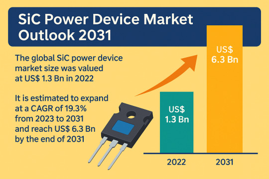
Automotive and Renewable Energy Sectors Power Global SiC Device Market Expansion
The global silicon carbide (SiC) power device market was valued at US$ 1.3 billion in 2022 and is projected to expand at a robust CAGR of 19.3% from 2023 to 2031, reaching an estimated US$ 6.3 billion by the end of 2031, according to the latest industry analysis. SiC devices, known for their high efficiency, low power loss, and durability in high-voltage and high-temperature conditions, are increasingly being adopted across automotive, industrial, renewable energy, and consumer electronics sectors.
Market Overview
SiC power devices have emerged as a critical solution for next-generation power electronics, offering significant improvements over traditional silicon-based components. With the ability to reduce power loss, increase switching speed, and operate under higher temperatures and voltages, SiC semiconductors are transforming industries that demand high reliability and energy efficiency.
Their unique material characteristics are particularly beneficial in wide bandgap applications, where reducing system size, weight, and cost are essential. The automotive industry, especially the electric vehicle (EV) segment, is a primary adopter, leveraging SiC to improve vehicle performance and energy efficiency.
Market Drivers & Trends
The growing push toward electrification, decarbonization, and energy efficiency is propelling the demand for SiC power devices globally. Key market drivers include:
Rising demand for high-efficiency power systems in industrial and renewable energy applications.
Accelerated EV adoption, requiring robust power electronics for traction inverters, battery chargers, and onboard systems.
Reduction in system size and complexity, thanks to superior properties of SiC MOSFETs and diodes.
Government incentives and mandates for cleaner transportation and energy storage systems.
These trends align with global sustainability goals, where power efficiency and reduced carbon footprint are paramount.
Latest Market Trends
SiC MOSFETs Dominate the Market: Representing over 32% of global share in 2022, the MOSFET segment continues to gain traction due to its high reliability, critical breakdown strength, and thermal performance.
600V–1000V Segment Leading by Voltage Range: With 31.89% share in 2022, this voltage range supports applications such as solar inverters, UPS systems, EV charging, and industrial drives.
High Power Modules in EV Applications: Companies like STMicroelectronics and WOLFSPEED have introduced SiC modules aimed at improving the driving range and energy management of electric vehicles.
Download Sample PDF Copy Now: https://www.transparencymarketresearch.com/sample/sample.php?flag=S&rep_id=22034
Key Players and Industry Leaders
The SiC power device market is consolidated, with a few dominant players accounting for a majority of the market share. These include:
Coherent Corp.
Fuji Electric Co., Ltd
Infineon Technologies AG
Microchip Technology Inc.
Mitsubishi Electric Corporation
ON Semiconductor Corp
Renesas Electronics Corporation
ROHM Co., Ltd
Toshiba Electronic Devices & Storage Corporation
WOLFSPEED, INC.
These companies are investing heavily in R&D, expanding wafer production capabilities, and launching new product lines to meet surging demand.
Recent Developments
Mitsubishi Electric (March 2023): Constructed a new wafer facility to meet soaring demand for SiC power semiconductors.
Toshiba (December 2022): Developed advanced SiC MOSFETs with enhanced reliability and low resistance.
Microchip Technology (March 2022): Unveiled 3.3 kV SiC power devices for next-generation renewable energy and transportation solutions.
STMicroelectronics: Launched SiC high-power modules for EV traction systems in December 2022.
Market Opportunities
Emerging opportunities include:
Electrification of transportation: As EV adoption scales, SiC’s role becomes more critical in powertrain efficiency.
Expansion in renewable energy and grid infrastructure: Solar and wind energy systems benefit from SiC’s efficiency and reliability.
Adoption in aerospace and defense sectors: Where lightweight, high-performance power systems are increasingly necessary.
High-growth emerging economies in Asia-Pacific and Latin America provide untapped potential for SiC deployment.
Future Outlook
By 2031, the SiC power device market will be defined by:
Continued penetration into mainstream automotive platforms, including hybrid and electric vehicles.
Broad industrial adoption of SiC for high-efficiency motor drives, UPS, and energy storage.
Increased investment in supply chain capacity and localized SiC wafer manufacturing, especially in Asia and North America.
Analysts emphasize the role of SiC in enabling sustainable energy systems and expect the technology to be foundational to next-gen power semiconductors.
Market Segmentation
By Product Type:
Diode
Power Module
MOSFETs
Gate Driver
By Voltage:
Up to 600V
600V – 1000V
1000V – 1500V
Above 1500V
By Application:
Inverter / Converter
Power Supply
Motor Drive
Photovoltaic / Energy Storage Systems
Flexible AC Transmission Systems (FACTs)
RF Devices & Cellular Base Stations
Others (Traction Systems, Induction Heating)
By End-use Industry:
Automotive & Transportation
Aerospace & Defense
Consumer Electronics
IT & Telecommunication
Others (Healthcare, Energy & Utility)
Regional Insights
Asia Pacific held the largest market share (44.23%) in 2022 due to high demand from the electronics, automotive, and industrial sectors in countries like China, Japan, and India. Government policies supporting EV adoption and renewable energy integration are also fostering market growth.
North America (26.12% share) is poised for strong growth, with major semiconductor companies investing in product innovation and strategic partnerships. The U.S. remains a hub for electric vehicle innovation and renewable power generation.
Europe continues to strengthen its position through green energy mandates and rapid EV expansion in countries like Germany and the U.K.
Why Buy This Report?
Comprehensive Market Coverage: Includes qualitative and quantitative analysis with segment-wise and region-wise forecasts.
Strategic Insights: Covers key drivers, trends, and market dynamics shaping the SiC power device industry.
Competitive Intelligence: Profiles leading companies and details on recent innovations, partnerships, and expansions.
Decision-Making Support: Aids industry stakeholders in understanding growth opportunities and market trajectories to align their strategies accordingly.
Customizable Format: Available in PDF and Excel with deep-dive access to historical and projected data.
0 notes
Text
Solar and Electronic Grade Polysilicon Market Growth Analysis 2025
As of 2024, the global Solar and Electronic Grade Polysilicon Market is valued at approximately USD 32.84 billion. Projections indicate that the market will reach USD 44.91 billion by 2032, growing at a Compound Annual Growth Rate (CAGR) of 4.2% during the forecast period from 2025 to 2032.
Get free sample of this report at : https://www.intelmarketresearch.com/download-free-sample/898/Solar-and-Electronic-Grade-Polysilicon-Market
The global Solar and Electronic Grade Polysilicon market plays a crucial role in the advancement of renewable energy and high-tech electronics industries. The production of polysilicon involves processes like the Siemens method and Fluidized Bed Reactor (FBR) technology, which purify metallurgical-grade silicon into high-purity polysilicon. This purified polysilicon is then formed into ingots, sliced into wafers, and further processed into solar cells or semiconductor components. The demand for solar-grade polysilicon has increased dramatically due to the growing global emphasis on sustainable technologies and clean energy, as well as the quick global adoption of solar photovoltaic (PV) systems.Electronic-grade polysilicon is also necessary for the production of microchips and integrated circuits, which supports the expansion of the semiconductor industry. This market is a major enabler of the green energy transition because manufacturers are able to meet the growing demand for high-quality polysilicon with strict purity requirements because of innovations in production processes and capacity expansion.
Market Dynamics (Drivers, Restraints, Opportunities, and Challenges)
Drivers
Rapid Expansion of Solar Energy Installations
The global solar and electronic grade polysilicon market is experiencing significant growth, primarily driven by the rapid expansion of solar energy installations worldwide. According to International Energy Agency, in 2024, global photovoltaic (PV) capacity reached over 2.2 terawatts (TW), up from 1.6 TW in 2023, with more than 600 gigawatts (GW) of new PV systems commissioned during the year. China installed up to 357.3 GW, accounting for almost 60% of new global capacity. Outside China, 244.6 GW were added, led by the European Union (62.6 GW), USA (47.1 GW), and India (31.9 GW).This surge in solar installations is expected to continue, with projections indicating that the world could be installing 1 TW of solar capacity annually by the end of the decade . As the demand for high-efficiency solar cells increases, so does the need for high-purity polysilicon, a critical material in solar panel manufacturing. This trend underscores the pivotal role of polysilicon in supporting the global transition to renewable energy
Restraints
High Production Costs and Supply Chain Constraints
The high cost of production and continuous supply chain issues are two major factors impeding the expansion of the global market for solar and electronic grade polysilicon. Energy-intensive procedures like the Siemens method are needed to produce ultra-high-purity polysilicon, which raises manufacturing costs dramatically. The U.S. Department of Energy estimates that energy use makes up almost 40% of the total cost of producing polysilicon. Furthermore, recent energy price swings and disruptions in the supply of raw materials like metallurgical-grade silicon have resulted in volatile polysilicon prices, which have an impact on downstream manufacturers' affordability and profitability. These factors can slow capacity expansion and delay project timelines, especially for smaller producers and emerging markets, creating a barrier to faster market growth.
Opportunities
Expansion of Polysilicon Production in Emerging Economies
The expansion of manufacturing capacities in emerging economies, especially in India and Southeast Asia, is creating new growth opportunities for the global polysilicon market. To lessen reliance on imports and encourage the use of clean energy, governments in these areas are making significant investments in domestic solar manufacturing. To encourage integrated polysilicon-to-module production, for instance, the Indian government introduced the Production-Linked Incentive (PLI) program in 2023 with ₹19,500 crore (about $2.4 billion). Large-scale polysilicon facilities are being established by companies like Adani and Reliance with the goal of establishing an independent solar ecosystem. In addition to diversifying the global supply chain, which has historically been controlled by China, this trend also creates jobs, expands regional markets, and aids in the global transition to renewable energy.
Regional Analysis
The Asia-Pacific region dominates the global polysilicon market, accounting for approximately 64% of the market share in 2024. This dominance is primarily due to China's significant production capacity, which produced 857,000 tons of polysilicon in 2022, representing 86% of global production.
North America and Europe also contribute significantly to the market, driven by technological advancements and increasing investments in renewable energy. The Middle East and Africa are emerging as fast-growing regions, with a projected CAGR of 9-11%, fueled by investments in solar energy infrastructure.
Competitor Analysis (in brief)
The global polysilicon market is characterized by the presence of several key players:
Wacker Chemie AG: A leading German chemical company with advanced production facilities and a strong focus on sustainability.
OCI Company Ltd.: A South Korean company known for its significant production capacity and strategic partnerships.
GCL-Poly Energy Holdings Limited: One of China's largest polysilicon producers, contributing substantially to the global supply.
Daqo New Energy Corp.: A Chinese company specializing in high-purity polysilicon for the solar PV industry.
REC Silicon ASA: A Norwegian company with a focus on sustainable polysilicon production.
These companies are actively engaged in expanding their production capacities, investing in research and development, and forming strategic alliances to strengthen their market positions.
In August 2024, Chinese solar giant Tongwei announced the acquisition of a majority stake in Runergy for about $700 million. Consolidating China's oversupplied solar industry was the goal of this move. But Tongwei's financial troubles, which included a 2.3 billion yuan net loss in the second quarter of 2024 and a decline in gross profit margin to 5%, have cast doubt on the acquisition's feasibility.
In May 2024, Elkem ASA, a Norwegian company, REC Solar for $22 million. By utilising REC Solar's technology and experience to increase its renewable energy offerings, this acquisition is anticipated to strengthen Elkem's position in the solar energy industry.
In August 2024, Mississippi Silicon, a manufacturer of raw silicon metal based in the United States, partnered with REC Silicon, a polysilicon manufacturer based in Norway. This partnership, which comes after Hanwha Group invested in REC Silicon, intends to support the growth of an all-encompassing U.S. solar supply chain that includes the processing of raw silicon, the manufacturing of polysilicon, and the assembly of solar modules.
In August 2023, Tokuyama Corp. of Japan and OCI Co. of South Korea announced a joint venture to produce polysilicon semiconductors in Malaysia. The goal of this collaboration is to increase the availability of high-purity polysilicon for use in electronics and solar power.Tokuyama Corp. of Japan and OCI Co. of South Korea announced a joint venture to produce polysilicon semiconductors in Malaysia. The goal of this collaboration is to increase the availability of high-purity polysilicon for use in electronics and solar power.
Global Solar and Electronic Grade Polysilicon Market: Market Segmentation Analysis
This report provides a deep insight into the global Solar and Electronic Grade Polysilicon Market, covering all its essential aspects. This ranges from a macro overview of the market to micro details of the market size, competitive landscape, development trend, niche market, key market drivers and challenges, SWOT analysis, value chain analysis, etc.
The analysis helps the reader to shape the competition within the industries and strategies for the competitive environment to enhance the potential profit. Furthermore, it provides a simple framework for evaluating and assessing the position of the business organization. The report structure also focuses on the competitive landscape of the Global Solar and Electronic Grade Polysilicon Market. This report introduces in detail the market share, market performance, product situation, operation situation, etc., of the main players, which helps the readers in the industry to identify the main competitors and deeply understand the competition pattern of the market.
In a word, this report is a must-read for industry players, investors, researchers, consultants, business strategists, and all those who have any kind of stake or are planning to foray into the Solar and Electronic Grade Polysilicon Market in any manner.
Market Segmentation (by Grade Type)
Solar Grade Polysilicon
Electronic Grade Polysilicon
Market Segmentation (by Application)
Solar Grade Applications
Photovoltaic (PV) Cells
Solar Modules & Panels
Electronic Grade Applications
Semiconductor Wafers (Silicon wafers for chips)
Integrated Circuits (ICs)
Microelectronics & MEMS
LEDs & Optoelectronics
Market Segmentation (by End-Use Industry)
Solar Energy (PV Industry)
Electronics & Semiconductors
Aerospace & Defense
Automotive
Key Company
Wacker Chemie AG
OCI Company Ltd.
GCL-Poly Energy Holdings Limited
Daqo New Energy Corp.
REC Silicon ASA
Tokuyama Corporation
Hemlock Semiconductor Corporation
Mitsubishi Materials Corporation
Sinosico
Huanghe Hydropower
Yichang CSG
Xinte Energy
East Hope
Xinjiang DAQO
Asia Silicon (Qinghai)
Tongwei Co., Ltd.
Dongli Silicon
Geographic Segmentation
North America: United States, Canada, Mexico
Europe: Germany, France, United Kingdom, Italy, Russia, Nordic Countries, Benelux, Rest of Europe
Asia: China, Japan, South Korea, Southeast Asia, India, Rest of Asia
South America: Brazil, Argentina, Rest of South America
Middle East & Africa: Turkey, Israel, Saudi Arabia, United Arab Emirates, Rest of Middle East & Africa
FAQs: Solar and Electronic Grade Polysilicon Market
Q1. What is the current size of the global Solar and Electronic Grade Polysilicon market?
As of 2024, the global Solar and Electronic Grade Polysilicon market is valued at approximately USD 32.84 billion.
Q2. What is the projected market size by 2032?
The market is expected to reach around USD 44.91 billion by 2032, growing at a CAGR of 4.2% from 2025 to 2032.
Q3. What are the primary applications of solar and electronic grade polysilicon?
The market is segmented by application into:
Solar Use: Utilized in photovoltaic (PV) cells for solar energy systems.
Semiconductor Use: Used in the manufacturing of semiconductors for electronics and computing devices.
Q4. Which application segment held the largest market share in 2023?
The solar use segment accounted for about 65% of the market in 2023, driven by the surge in global solar energy installations.
Q5. Which segment is expected to grow the fastest during the forecast period?
The semiconductor use segment is anticipated to grow at the fastest rate, propelled by increasing demand for chips and electronic devices.
Get free sample of this report at : https://www.intelmarketresearch.com/download-free-sample/898/Solar-and-Electronic-Grade-Polysilicon-Market
0 notes
Text
EUV Pellicle Market : Size, Trends, and Growth Analysis 2032
EUV Pellicle Market: Protecting the Future of Semiconductor Lithography
The EUV Pellicle Market size was valued at US$ 590.43 Million in 2024 and is forecasted to grow at a robust CAGR of 14.90% from 2025 to 2032. EUV pellicles are becoming increasingly critical in the semiconductor manufacturing process as the industry pushes the boundaries of miniaturization and chip performance.
What is an EUV Pellicle?
An Extreme Ultraviolet (EUV) pellicle is an ultra-thin, highly transparent membrane film designed to protect photomasks during EUV lithography. Photomasks carry the intricate circuit patterns that need to be etched onto semiconductor wafers. Because EUV lithography uses light at a wavelength of 13.5 nm—much shorter than traditional lithography wavelengths—the precision required is extreme, and even microscopic particles can cause significant defects in the wafer patterns.
The EUV pellicle acts as a physical barrier, preventing dust, contaminants, and particles from settling on the photomask surface. It allows EUV light to pass through with minimal absorption or distortion while ensuring the photomask remains uncontaminated, thereby enhancing yield rates and reducing costly reworks.
Market Drivers
1. Shrinking Node Sizes and Advanced Semiconductor Fabrication As semiconductor manufacturers push towards smaller technology nodes (sub-7 nm and below), the precision requirements for lithography increase exponentially. EUV lithography is pivotal to these advancements, and the demand for reliable EUV pellicles to protect photomasks grows correspondingly.
2. Increasing Demand for High-Performance Electronics The rising adoption of AI, IoT, 5G, and automotive electronics necessitates chips with higher transistor densities and superior performance. This trend drives investments in advanced lithography solutions where EUV pellicles are indispensable.
3. Growing Semiconductor Industry Investment Significant capital investments by semiconductor fabrication plants (fabs) in the U.S., South Korea, Taiwan, and China are accelerating the adoption of EUV lithography equipment. Consequently, the demand for supporting components like pellicles is on the rise.
4. Need for Yield Improvement and Cost Reduction Photomask defects due to particle contamination can cause substantial production losses. EUV pellicles improve yields by minimizing contamination risks, helping fabs reduce scrap rates and overall manufacturing costs.
Technical Challenges and Innovations
Material Selection and Durability EUV pellicles must be ultra-thin yet mechanically robust, withstand high EUV light intensities without degradation, and maintain thermal and chemical stability during lithography. The choice of pellicle materials such as silicon-based membranes or specialized polymers is critical to achieving these performance metrics.
Transparency and Low Absorption Because EUV light has high energy, even slight absorption or reflection by the pellicle can affect lithography quality. Innovations in material engineering aim to enhance pellicle transparency above 90%, reducing light loss and pattern distortion.
Thermal Management EUV lithography exposes pellicles to high thermal loads. Effective heat dissipation techniques and materials with high thermal stability are under continuous development to prevent pellicle damage and maintain performance.
Market Segmentation
By Product Type:
Silicon-based Pellicles
Polymer-based Pellicles
Composite Pellicles
By End-Use:
Semiconductor Foundries
Chip Manufacturers
Research and Development Institutes
By Region:
Asia-Pacific
North America
Europe
Rest of the World
Asia-Pacific dominates due to the concentration of semiconductor manufacturing hubs in countries like Taiwan, South Korea, and China. North America and Europe maintain significant shares driven by technology innovation and fab expansions.
Competitive Landscape
The EUV pellicle market is characterized by a few leading players with advanced technological capabilities and strong R&D investments:
ASML Holding N.V. As the pioneer of EUV lithography systems, ASML plays a critical role in the pellicle market through strategic partnerships and in-house development. Its integration of pellicles in EUV scanners enhances lithography precision.
Mitsui Chemicals, Inc. Known for its innovation in high-performance materials, Mitsui Chemicals produces cutting-edge pellicle films designed for enhanced durability and transparency in EUV applications.
Shin-Etsu Chemical Co., Ltd. Shin-Etsu specializes in advanced semiconductor materials and offers pellicle products engineered for high thermal stability and low EUV absorption.
FUJIFILM Holdings Corporation With a strong presence in thin-film technology, FUJIFILM manufactures pellicles with superior mechanical strength and chemical resistance.
Toppan Inc. Toppan’s expertise in photomask production complements its development of pellicle solutions aimed at minimizing contamination and improving semiconductor yield.
SÜSS MicroTec SE A key player in lithography equipment and photomask technologies, SÜSS MicroTec provides specialized pellicle handling and integration systems.
Industry Outlook
The EUV pellicle market is set to benefit from the global semiconductor industry's unrelenting focus on miniaturization and yield optimization. As fabs increase EUV scanner deployment, demand for pellicles will scale accordingly. Advances in materials science and thermal management will continue to unlock pellicle performance improvements, expanding their adoption.
Moreover, government initiatives worldwide to boost semiconductor self-reliance and chip manufacturing capacity are expected to create new growth opportunities for pellicle manufacturers. Collaborations between pellicle suppliers, lithography system makers, and semiconductor manufacturers are fostering innovation cycles that will push EUV lithography capabilities further.
Browse more Report:
Biostimulants Market
Multilayer Printed Circuit Board Market
Wafer Cases Market
Multimedia Chipsets Market
IoT Microcontroller Market
0 notes
Text
0 notes
Text
Semiconductor Grade Solvents Market, Global Outlook and Forecast 2025-2032
The global Semiconductor Grade Solvents Market is experiencing robust expansion, reaching a valuation of USD 2.68 billion in 2024. Industry forecasts project sustained growth at a 7.0% CAGR, pushing market value to USD 4.27 billion by 2031. This trajectory reflects the critical role of ultra-pure solvents in semiconductor fabrication, where even parts-per-trillion impurities can disrupt advanced chip manufacturing processes.
Semiconductor grade solvents represent the backbone of chip production, enabling precise wafer cleaning, photoresist stripping, and surface preparation. Their application spans across semiconductor manufacturing, display technologies, and photovoltaic production, with purity requirements tightening as process nodes shrink below 3nm. The industry's shift toward EUV lithography and 3D NAND architectures is further elevating solvent performance benchmarks.
Download FREE Sample Report: https://www.24chemicalresearch.com/download-sample/291173/semiconductor-grade-solvents-forecast-market
Market Overview & Regional Analysis
Asia-Pacific dominates semiconductor solvent consumption, accounting for over 50% of global demand. This concentration stems from Taiwan's advanced foundries, South Korea's memory chip hubs, and China's rapidly expanding semiconductor ecosystem. The region benefits from close proximity to major chip manufacturers and government initiatives like China's "Big Fund" investments in domestic semiconductor capabilities.
North America maintains strong market presence through its leading-edge semiconductor research and manufacturing clusters, while Europe sees steady demand from specialized semiconductor applications. Emerging markets in Southeast Asia show promise as new semiconductor fabrication plants diversify global supply chains, creating localized solvent demand.
Key Market Drivers and Opportunities
The market's expansion rides on multiple technological and economic currents. The proliferation of 5G infrastructure demands high-frequency chips requiring ultra-clean surfaces, while automotive electrification increases semiconductor content per vehicle by 40% compared to traditional models. Meanwhile, AI hardware development pushes the boundaries of chip complexity, necessitating next-generation solvent formulations.
Opportunities abound in advanced packaging solutions like chiplet architectures and fan-out wafer-level packaging, where specialized solvents enable higher-density interconnects. The parallel growth of compound semiconductors for power electronics opens new application pathways, particularly for solvents compatible with gallium nitride and silicon carbide processing.
Challenges & Restraints
Market growth faces headwinds from increasing environmental regulations governing solvent emissions and waste treatment. The industry must balance purity requirements with sustainability goals as REACH and similar frameworks tighten VOC restrictions. Supply chain vulnerabilities also persist, with critical solvent precursors sometimes concentrated in geopolitically sensitive regions.
Technical challenges intensify as process nodes shrink—today's 2nm technologies demand solvent purity levels that were theoretical a decade ago. The capital intensity of purification infrastructure creates barriers for new entrants, while lengthy qualification processes slow supplier diversification in this stringent market.
Market Segmentation
By Product Type
Ultra High Purity Reagents
Functional Chemicals
By Application
Wafer Cleaning
Photolithography
Etching Processes
Packaging Applications
Competitive Landscape
The market features a mix of global chemical conglomerates and specialized purity solution providers:
Mitsubishi Chemical
Entegris (CMC Materials)
Stella Chemifa
Avantor
BASF
Honeywell
TOKYO OHKA KOGYO
JSR Corporation
Report Coverage
This comprehensive market analysis examines:
Technology trends in solvent purification and delivery systems
Purity standard evolution across semiconductor generations
Regional capacity expansions and supply chain dynamics
Strategic initiatives by leading market participants
Get Full Report Here: https://www.24chemicalresearch.com/reports/291173/semiconductor-grade-solvents-forecast-market
About 24chemicalresearch
Founded in 2015, 24chemicalresearch has rapidly established itself as a leader in chemical market intelligence, serving clients including over 30 Fortune 500 companies. We provide data-driven insights through rigorous research methodologies, addressing key industry factors such as government policy, emerging technologies, and competitive landscapes.
Plant-level capacity tracking
Real-time price monitoring
Techno-economic feasibility studies
With a dedicated team of researchers possessing over a decade of experience, we focus on delivering actionable, timely, and high-quality reports to help clients achieve their strategic goals. Our mission is to be the most trusted resource for market insights in the chemical and materials industries.
International: +1(332) 2424 294 | Asia: +91 9169162030
Website: https://www.24chemicalresearch.com/
Follow us on LinkedIn: https://www.linkedin.com/company/24chemicalresearch
0 notes