#compound semiconductor wafer china
Text
Epitaxial Wafer Market Trends Growth by Innovation in LED lighting
The epitaxial wafer market plays a pivotal role in manufacturing high-performance semiconductor devices used in applications ranging from consumer electronics to advanced healthcare devices. Epitaxial wafers aid in developing sophisticated integrated circuits and semiconductor chips through epitaxial growth techniques. Advancements in LED technology have increased the demand for epitaxial wafers for commercial and industrial applications. The global epitaxial wafer market is expected to gain significant traction on account of rising adoption of LED lighting and displays.
The Epitaxial Wafer Market size was valued at USD 2,778 million in 2022 and is anticipated to witness a compound annual growth rate (CAGR) of 12.9% from 2022 to 2030.
Key players operating in the epitaxial wafer market are EpiWorks Inc., Global Wafers Japan Co. Ltd., Nichia Corporation, SHOWA DENKO K.K., Siltronic AG, Desert Silicon Inc., Electronics and Materials Corporation Ltd. Intelligent Epitaxy Technology Inc.IQE plc., Jenoptic AG, MOSPEC Semiconductor Corporation, Norstel AB, Ommic S.A., Silicon Valley Microelectronics Inc., SVT Associates Inc. Universal Wafer Inc., Wafer Works Corporation, Xiamen Powerway Advanced Materials Co. Ltd., and Visual Photonics Epitaxy Co. Ltd.
Key Takeaways
Key players: EpiWorks, Global Wafers Japan, and Nichia captured over 35% share of the global market in 2024. EpiWorks leads the market with its diversified product portfolio and strong customer base.
Growing demand: Rising adoption of LED lighting, increasing penetration of advanced displays in consumer electronics and mobile devices, and growth of the semiconductor industry will continue to boost demand for epitaxial wafers in the coming years.
Global expansion: Leading manufacturers are investing heavily in capacity expansion plans across China, Taiwan, Europe, and the US to cater to the growing worldwide demand. Strategic partnerships and joint ventures are also gaining traction.
Market key trends
The Epitaxial Wafer Market Trends is undergoing significant transformation led by technological innovation in LED lighting applications. Manufacturers are focusing on developing high-quality mono-epitaxial and multi-epitaxial wafers to enable the mass production of more energy-efficient LED bulbs, streetlights, lamps, and advanced display backlights. Additionally, continuous ramp-up in wafer sizes from 150mm to 200mm and above is helping chipmakers lower production costs and improve epitaxial growth yield. This shift towards larger and more advanced epitaxial wafer substrates will define future market trends.
Porter’s Analysis
Threat of new entrants: New companies find it difficult to enter this market as a significant capital investment and technical expertise is required to set up manufacturing facilities for epitaxial wafers.
Bargaining power of buyers: Large technology companies like Intel, TSMC, Samsung, etc have significant bargaining power over epitaxial wafer suppliers given their high purchase volumes.
Bargaining power of suppliers: The presence of many established players limits the bargaining power of suppliers in this market.
Threat of new substitutes: There are limited substitutes for epitaxial wafers as they enable performance and cost benefits for several semiconductor devices.
Competitive rivalry: The market is dominated by few global players who compete intensely on technology leadership, quality, and customer service.
Geographical Regions
Asia Pacific accounts for the major share of the global epitaxial wafer market in terms of value owing to presence of large semiconductor manufacturing facilities and foundries located in countries like China, Taiwan, South Korea and Japan.
North America is expected to witness the fastest growth during the forecast period due to expanding semiconductor industry and ongoing technological advancements in the region. Rising demand for advanced semiconductor devices from sectors such as consumer electronics, automotive, industrial will drive the epitaxial wafer market in this region.
Get more insights on Epitaxial Wafer Market
About Author:
Money Singh is a seasoned content writer with over four years of experience in the market research sector. Her expertise spans various industries, including food and beverages, biotechnology, chemical and materials, defense and aerospace, consumer goods, etc. (https://www.linkedin.com/in/money-singh-590844163)

#Coherent Market Insights#Epitaxial Wafer Market#Epitaxial Wafer#Semiconductor Wafer#Epitaxy#Silicon Wafer#Semiconductor Materials#Epitaxial Layer#Microelectronics
0 notes
Text
The Photoresist Chemicals market is projected to grow from USD 3,375.86 million in 2024 to USD 4,360.18 million by 2032, reflecting a compound annual growth rate (CAGR) of 3.25%.The photoresist chemicals market is undergoing a significant transformation, driven by the burgeoning demands of the semiconductor and electronics industries. Photoresist chemicals are light-sensitive materials used in photolithography and photoengraving processes to form a patterned coating on a surface. These chemicals play a critical role in the manufacturing of printed circuit boards (PCBs), microelectromechanical systems (MEMS), and integrated circuits (ICs), making them indispensable to modern technology.
Browse the full report at https://www.credenceresearch.com/report/photoresist-chemicals-market
Market Dynamics
The photoresist chemicals market is expected to witness robust growth in the coming years. Several factors contribute to this positive outlook:
1. Advancements in Semiconductor Technology: The continuous miniaturization of electronic devices necessitates more sophisticated and precise photolithography techniques. Photoresist chemicals are crucial in defining the intricate patterns on semiconductor wafers, enabling the production of smaller and more powerful chips.
2. Rising Demand for Consumer Electronics: The proliferation of smartphones, tablets, wearable devices, and other consumer electronics has led to increased production of semiconductors, thereby boosting the demand for photoresist chemicals.
3. Growth of the Automotive Industry: The automotive sector's shift towards electric and autonomous vehicles is driving the need for advanced electronic components, which rely heavily on photoresist chemicals for their manufacturing.
4. Expansion of the Internet of Things (IoT): The IoT ecosystem's growth is spurring the development of numerous connected devices, all of which require semiconductors produced using photoresist chemicals.
Types of Photoresist Chemicals
Photoresist chemicals are broadly categorized into three types based on their properties and applications:
1. Positive Photoresists: These chemicals become soluble when exposed to light, allowing the exposed areas to be washed away, leaving a patterned coating. They are preferred for their high resolution and precision in semiconductor manufacturing.
2. Negative Photoresists: These chemicals become insoluble when exposed to light, causing the unexposed areas to be washed away. They are typically used in applications requiring thick photoresist layers, such as MEMS fabrication.
3. DNQ-based Photoresists: Diazonaphthoquinone (DNQ)-based photoresists are widely used in the production of PCBs and ICs. They offer excellent resolution and are compatible with various etching processes.
Regional Insights
The photoresist chemicals market is globally segmented into North America, Europe, Asia-Pacific, and the rest of the world. Among these regions, Asia-Pacific dominates the market, driven by the presence of major semiconductor manufacturing hubs in countries like China, Japan, South Korea, and Taiwan. The region's strong electronics manufacturing infrastructure and significant investments in semiconductor fabs contribute to its market leadership.
North America is another key market, with the United States being home to several leading semiconductor companies and research institutions. The region's focus on technological innovation and R&D activities fuels the demand for advanced photoresist chemicals.
Europe is also witnessing growth in the photoresist chemicals market, supported by the automotive industry's expansion and the increasing adoption of IoT devices. Countries like Germany and France are at the forefront of this growth, with strong semiconductor manufacturing capabilities.
Competitive Landscape
The photoresist chemicals market is highly competitive, with several key players vying for market share. Some of the prominent companies include:
1. Tokyo Ohka Kogyo Co., Ltd.: A leading manufacturer of photoresist chemicals, known for its innovative solutions and extensive product portfolio.
2. JSR Corporation: Specializes in high-performance photoresists used in semiconductor manufacturing.
3. Dow Chemical Company: Offers a range of advanced photoresist materials for various applications.
4. Fujifilm Holdings Corporation: Provides cutting-edge photoresist chemicals and has a strong presence in the global market.
5. Sumitomo Chemical Co., Ltd.: Known for its high-quality photoresist products used in electronics manufacturing.
Future Outlook
The future of the photoresist chemicals market looks promising, with continuous advancements in semiconductor technology and the growing adoption of electronic devices. Innovations in photolithography techniques, such as extreme ultraviolet (EUV) lithography, are expected to drive the demand for more sophisticated photoresist chemicals.
Moreover, the increasing focus on sustainability and environmental regulations is pushing manufacturers to develop eco-friendly photoresist solutions. This trend is likely to create new opportunities for companies that can offer green alternatives without compromising performance.
Key Player Analysis
FUJIFILM Corporation
TOKYO OHKA KOGYO CO., LTD.
I. DuPont de Nemours
JSR Corporation
Dow
Mitsui Chemicals America Inc
LG Chem
Shin-Etsu Chemical Co., Ltd.
TOK America
Honsou Chemical Industry
Segments:
Based on Product Type:
Positive
Negative
Based on Spectral Line Size:
G-line
I-line
KrF (Krypton Fluoride)
ArF immersion (Argon Fluoride Immersion)
ArF dry (Argon Fluoride Dry)
Based on End Use Applications:
Microelectronics
Sand carving
Fabrication of printed circuit boards
Based on the Geography:
North America
US
Canada
Mexico
Europe
Germany
France
UK
Italy
Spain
Rest of Europe
Asia Pacific
China
Japan
India
South Korea
South-east Asia
Rest of Asia Pacific
Latin America
Brazil
Argentina
Rest of Latin America
Middle East & Africa
GCC Countries
South Africa
Rest of Middle East and Africa
Browse the full report at https://www.credenceresearch.com/report/photoresist-chemicals-market
About Us:
Credence Research is committed to employee well-being and productivity. Following the COVID-19 pandemic, we have implemented a permanent work-from-home policy for all employees.
Contact:
Credence Research
Please contact us at +91 6232 49 3207
Email: [email protected]
Website: www.credenceresearch.com
0 notes
Text
Semiconductor Sensors Market Analysis 2023 Dynamics, Players, Type, Applications, Trends, Regional Segmented, Outlook & Forecast till 2033
The semiconductor sensor market is expected to grow at a compound annual growth rate (CAGR) of 10.41% from 2024 to 2033, reaching a value of $319.6 billion by 2033. This is based on the 2023 market size of $201 billion.
The competitive analysis of the Semiconductor Sensors Market offers a comprehensive examination of key market players. It encompasses detailed company profiles, insights into revenue distribution, innovations within their product portfolios, regional market presence, strategic development plans, pricing strategies, identified target markets, and immediate future initiatives of industry leaders. This section serves as a valuable resource for readers to understand the driving forces behind competition and what strategies can set them apart in capturing new target markets.
Market projections and forecasts are underpinned by extensive primary research, further validated through precise secondary research specific to the Semiconductor Sensors Market. Our research analysts have dedicated substantial time and effort to curate essential industry insights from key industry participants, including Original Equipment Manufacturers (OEMs), top-tier suppliers, distributors, and relevant government entities.
Semiconductor Sensors Market Benefits
Semiconductor Sensors research reports provide critical insights for strategic decision-making. They help businesses understand market trends, customer preferences, and competitive landscapes. By analyzing data on market size, growth potential, and consumer behavior, companies can identify new opportunities and mitigate risks. These reports also guide product development, pricing strategies, and marketing campaigns, ensuring alignment with current market demands. Furthermore, market research reports enhance forecasting accuracy and help in benchmarking performance against competitors. Ultimately, they inform investment decisions, optimize resource allocation, and foster innovation, contributing to sustained business growth and a competitive edge.
Key Report Highlights:
Key Market Participants: The report delves into the major stakeholders in the market, encompassing market players, suppliers of raw materials and equipment, end-users, traders, distributors, and more.
Comprehensive Company Profiles: Detailed company profiles are provided, offering insights into various aspects including production capacity, pricing, revenue, costs, gross margin, sales volume, sales revenue, consumption patterns, growth rates, import-export dynamics, supply chains, future strategic plans, and technological advancements. This comprehensive analysis draws from a dataset spanning 12 years and includes forecasts.
Market Growth Drivers: The report extensively examines the factors contributing to market growth, with a specific focus on elucidating the diverse categories of end-users within the market.
Data Segmentation: The data and information are presented in a structured manner, allowing for easy access by market player, geographical region, product type, application, and more. Furthermore, the report can be tailored to accommodate specific research requirements.
SWOT Analysis: A SWOT analysis of the market is included, offering an insightful evaluation of its Strengths, Weaknesses, Opportunities, and Threats.
Expert Insights: Concluding the report, it features insights and opinions from industry experts, providing valuable perspectives on the market landscape.
Receive the FREE Sample Report of Semiconductor Sensors Market Research Insights @ https://stringentdatalytics.com/sample-request/semiconductor-sensors-market/9492/
Market Segmentations:
Global Semiconductor Sensors Market: By Company
• Figaro
• Honeywell
• Nissha
• Amphenol
• New Cosmos Electric
• Alphasense
• Sensorix
• MGK Sensor
• Shanghai AICI
• China Wafer Level CSP
• Zhengzhou Winsen
Global Semiconductor Sensors Market: By Type
• Temperature Sensor
• Pressure Sensor
• Humidity Sensor
• Gas Sensor
• Others
Global Semiconductor Sensors Market: By Application
• Industrial Automation
• Household Appliance
• Environmental Monitoring
• Medical
• Automobile
• Others
Regional Analysis of Global Semiconductor Sensors Market
All the regional segmentation has been studied based on recent and future trends, and the market is forecasted throughout the prediction period. The countries covered in the regional analysis of the Global Semiconductor Sensors market report are U.S., Canada, and Mexico in North America, Germany, France, U.K., Russia, Italy, Spain, Turkey, Netherlands, Switzerland, Belgium, and Rest of Europe in Europe, Singapore, Malaysia, Australia, Thailand, Indonesia, Philippines, China, Japan, India, South Korea, Rest of Asia-Pacific (APAC) in the Asia-Pacific (APAC), Saudi Arabia, U.A.E, South Africa, Egypt, Israel, Rest of Middle East and Africa (MEA) as a part of Middle East and Africa (MEA), and Argentina, Brazil, and Rest of South America as part of South America.
Click to Purchase Semiconductor Sensors Market Research Report @ https://stringentdatalytics.com/purchase/semiconductor-sensors-market/9492/
Report includes Competitor's Landscape:
➊ Major trends and growth projections by region and country
➋ Key winning strategies followed by the competitors
➌ Who are the key competitors in this industry?
➍ What shall be the potential of this industry over the forecast tenure?
➎ What are the factors propelling the demand for the Semiconductor Sensors?
➏ What are the opportunities that shall aid in significant proliferation of the market growth?
➐ What are the regional and country wise regulations that shall either hamper or boost the demand for Semiconductor Sensors?
➑ How has the covid-19 impacted the growth of the market?
➒ Has the supply chain disruption caused changes in the entire value chain?
Why to Purchase Semiconductor Sensors Market Report?
Purchasing a market research report provides valuable, reliable insights that are often beyond a company's in-house capabilities. These reports deliver comprehensive data on market trends, customer behaviors, competitive analysis, and industry forecasts, saving time and resources on extensive data collection and analysis. They offer expert perspectives and methodologies, ensuring credible, up-to-date information. By accessing tailored, actionable intelligence, businesses can make informed decisions, reduce uncertainty, and identify opportunities for growth. Additionally, these reports enhance strategic planning, risk management, and competitive positioning, making them a crucial investment for companies seeking to stay ahead in their industry and drive innovation.
Customization of the Report:
This report can be customized to meet the client’s requirements. Please connect with our sales team ([email protected] ), who will ensure that you get a report that suits your needs. You can also get in touch with our executives on +1 346 666 6655 to share your research requirements.
About Stringent Datalytics
Stringent Datalytics offers both custom and syndicated market research reports. Custom market research reports are tailored to a specific client's needs and requirements. These reports provide unique insights into a particular industry or market segment and can help businesses make informed decisions about their strategies and operations.
Syndicated market research reports, on the other hand, are pre-existing reports that are available for purchase by multiple clients. These reports are often produced on a regular basis, such as annually or quarterly, and cover a broad range of industries and market segments. Syndicated reports provide clients with insights into industry trends, market sizes, and competitive landscapes. By offering both custom and syndicated reports, Stringent Datalytics can provide clients with a range of market research solutions that can be customized to their specific needs.
Reach US
Stringent Datalytics
+1 346 666 6655
Social Channels:
Linkedin | Facebook | Twitter | YouTube
0 notes
Text
Semiconductor Packaging Materials Market - Forecast(2024 - 2030)
Semiconductor packaging materials market size is forecast to reach USD 39,600 million by 2029, after growing at a CAGR of 9.79% during 2024-2029. By supplying the materials required for the assembly and packaging of semiconductor devices, the semiconductor packaging materials market is vital to the semiconductor industry. Substrates, leadframes, encapsulants, bonding wires, and die attach materials are a few examples of these materials. Technological developments, consumer demand for more compact and energy-efficient electronics, and the emergence of new technologies like IoT, artificial intelligence, and automotive electronics all have an impact on the market. With the development of cutting-edge packaging technologies like Chip-on-Wafer-on-Substrate (CoWoS) and Integrated Fan-Out (InFO), TSMC has been in the forefront of enabling the integration of numerous chips into a single package. Samsung has made investments in the creation of System-in-Package (SiP) solutions, which provide high-performance, small-form factor packaging choices for a range of uses, such as automotive electronics and mobile devices.
United States: To improve national security and advance domestic semiconductor manufacturing capabilities, the U.S. government has funded research and development initiatives in semiconductor packaging materials through the Department of Defense (DoD) and the National Science Foundation (NSF). Japan: As part of its plan to support the nation's semiconductor industry and preserve its position as a global leader, the Japanese government has announced investments in semiconductor R&D, including packaging technology.
Request Sample
Report Coverage
The report “Semiconductor packaging materials Market– Forecast (2024-2029)”, by IndustryARC, covers an in-depth analysis of the following segments of the semiconductor packaging materials market.
By Type: Substrates, Lead Frames, Bonding Wires, Mold Compounds, Liquid Encapsulants, Die Attach Materials, Solder Balls, Wafer-Level Package Dielectrics, and Plating ChemicalsBy Technology: Grid Array, System-In-Package (SIP), Quad Flat Package (QFP), Dual In-line Package, OthersBy End-User Industry: Consumer Electronics, Aerospace & Defense, Healthcare, Automotive, OthersBy Geography: North America, South America, Europe, Asia-Pacific, RoW
Key Takeaways
• Rapid technological breakthroughs are driving constant innovation in the semiconductor packaging materials market to fulfill the changing needs of the electronics sector. Chiplets and 3D stacking are two examples of cutting-edge packaging technology that businesses like Intel Corporation have been investing in. For example, Intel's "Foveros" technology allows numerous logic chips to be stacked vertically, which improves performance and power efficiency in small form factors.• The market for semiconductor packaging materials is dominated by the Asia-Pacific area, namely by nations like China, Japan, South Korea, and Taiwan, but new regional competitors are gaining ground on them. Packaging materials are only one area in which China's Semiconductor Manufacturing International Corporation (SMIC) has been growing its footprint in the semiconductor industry. SMIC's investments in cutting-edge packaging technologies are intended to strengthen homegrown semiconductor manufacturing capacities and lessen reliance on imports.• In the market for semiconductor packaging materials, sustainability is receiving more attention as businesses and governments place more emphasis on the creation and uptake of environmentally responsible packaging options. Regulations and incentives are part of the European Union's "Green Deal" plan to encourage environmentally friendly practices in the electronics sector. Businesses such as Infineon Technologies AG are allocating resources towards environmentally sustainable packaging materials and manufacturing techniques in order to meet regulatory obligations and satisfy consumer demand for sustainable products.
By Type - Segment AnalysisMold Compounds dominated the semiconductor packaging materials market in 2023. Mold compounds are essential for maintaining the dependability and durability of semiconductor devices because they shield sensitive parts from outside impurities and mechanical harm. Mold compounds are essential for a wide range of semiconductor devices since they are employed in a variety of packing technologies, such as conventional leaded packages and cutting-edge packages like chip-scale packages (CSPs), flip-chip packages, and ball grid arrays (BGAs). As sophisticated semiconductor packing technologies have become more complex, materials with increased dependability, less warpage, and higher thermal conductivity have been developed as a result of ongoing innovation in mold compound formulations. A new generation of mold compounds with improved temperature management capabilities has been developed, according to a recent announcement from prominent chemical manufacturer BASF SE. These cutting-edge materials meet the increasing need for high-performance semiconductor packages in industries including data centers, automotive electronics, and 5G infrastructure by providing exceptional thermal conductivity and dependability.
Buy Now
By Technology - Segment AnalysisSystem-in-Package (SiP) dominated the semiconductor packaging materials market in 2023. System-in-Package (SiP), one of the aforementioned semiconductor packaging technologies, has dominated the market share in recent years because of its adaptability and capacity to combine several functions into a single package. SiP is well-suited for a variety of applications in consumer electronics, telecommunications, automotive, and Internet of Things devices because it has a number of benefits over conventional packaging technologies. The development of InFO_SoW (System-on-Wafer), TSMC's sophisticated Integrated Fan-Out (InFO) packaging technology, was unveiled. This method enables high-density packing with better performance and a smaller form factor by integrating several chips and passive components on a single wafer. With its substantial cost, performance, and time-to-market benefits, InFO_SoW is a top option for upcoming electronic products.
By End User Industry - Segment AnalysisAutomotive Sector dominated the semiconductor packaging materials market in 2023. Because electronics are being integrated into cars more and more, the automobile sector has become a significant user of semiconductor packaging materials. Electric vehicle (EV) powertrains, infotainment systems, advanced driver assistance systems (ADAS), and vehicle connection are just a few of the many uses for semiconductor devices in modern cars. An important recent development that emphasizes the automobile sector's reliance on semiconductor technologies is Nvidia's acquisition of Arm Holdings. Nvidia, which is well-known for its proficiency with artificial intelligence (AI) and graphics processing units (GPUs), hopes to increase its market share in the car industry by utilizing Arm's chip design skills. The significance of semiconductor packaging materials in allowing cutting-edge computing systems for connected and autonomous automobiles is highlighted by this acquisition.
By Geography - Segment AnalysisAsia Pacific dominated the semiconductor packaging materials market in 2023. Due to a number of factors, including the existence of important semiconductor manufacturers, the high demand for consumer electronics, and government support for the semiconductor industry, Asia-Pacific has been the dominating region in the market for semiconductor packaging materials. Samsung Electronics made an announcement in South Korea on a large investment in its semiconductor industry, which included the creation of cutting-edge packaging technology. In order to better address the development of innovative packaging solutions for 5G, AI, and automotive applications, Samsung has expanded its System LSI division. This investment strengthens the region's standing as a global leader in the semiconductor industry and highlights its dedication to technological innovation.
Drivers – Semiconductor packaging materials Market
• Technological Advancements and MiniaturizationThe semiconductor industry's constant technological developments fuel the demand for electronic gadgets that are increasingly compact, potent, and energy-efficient. The adoption of cutting-edge packaging materials and solutions is fueled by this need for miniaturization. Manufacturers of semiconductors are under pressure to create novel packaging methods as consumers want electronic devices that are progressively more feature-rich and compact. Wafer-level packaging, 3D integration, and fan-out packaging are some of these methods that allow for increased component density and better performance in smaller form factors.Fan-out wafer-level packaging (FOWLP) has become more popular as a vital component of advanced packaging in recent years. The partnership between Advanced Semiconductor Engineering, Inc. (ASE) and Deca Technologies to create cutting-edge FOWLP solutions is an illustration of a real-time development. Through this collaboration, Deca's M-Series technology and ASE's experience in packaging technologies will be combined to provide high-performance, reasonably priced semiconductor packaging solutions for upcoming markets including 5G, AI, and Internet of Things devices.
• Increasing Demand for High-Performance ComputingThe increasing need for innovative semiconductor packaging materials that provide better electrical performance, thermal management, and durability is driven by the growing need for high-performance computing (HPC) applications, including data centers, artificial intelligence (AI), and automotive electronics. Semiconductor devices with increased processing power, memory bandwidth, and energy efficiency are needed for HPC applications. This calls for the creation of packaging materials with strong component interconnection, effective heat dissipation, and reduced signal loss. The semiconductor industry has seen a major real-time development with NVIDIA's acquisition of ARM Holdings. In order to create integrated solutions for AI, HPC, and automotive computing, NVIDIA—which is well-known for its GPUs used in HPC applications—aims to take advantage of ARM's experience in CPU and system-on-chip (SoC) design. The increasing significance of cutting-edge semiconductor packaging materials is demonstrated by this acquisition.
Challenges – Semiconductor packaging materials Market
• Miniaturization and ComplexityThe growing demand from consumers for more powerful, smaller electronic gadgets is a challenge for semiconductor packaging in terms of complexity and shrinking. Smaller semiconductor packages with the same or better performance require material and manufacturing process advances. Chiplets can now be integrated into a single package thanks to developments in Taiwan Semiconductor Manufacturing Company's (TSMC) InFO technology. This breakthrough solves the problem of shrinking while improving performance by enabling more functionality in smaller form factors.
• Thermal Management and ReliabilityAs semiconductor devices' power densities rise, reliability and thermal control have emerged as crucial packaging problems. Especially in high-performance applications, effective heat dissipation is crucial for preventing device failure and guaranteeing long-term reliability. For advanced packaging applications, Dow Inc. recently unveiled a unique mold compound with enhanced thermal conductivity and dependability. Because of this material's exceptional heat-dissipation qualities, semiconductor devices operate more dependably under hot conditions. When it comes to solving the problems associated with thermal management in semiconductor packing, this invention is a major step forward.
Market Landscape
Technology launches, acquisitions, and R&D activities are key strategies adopted by players in the semiconductor packaging materials market. Major players in the semiconductor packaging materials market are Dow Inc., Henkel AG & Co. KGaA, Sumitomo Chemical Co., Ltd., BASF SE, Hitachi Chemical Co., Ltd., Alent plc, Kyocera Chemical Corporation, Tanaka Holdings Co., Ltd., ASM Pacific Technology Ltd., and Shin-Etsu Chemical Co., Ltd. among others.
#Semiconductor Packaging Materials Market#Semiconductor Packaging Materials Market share#Semiconductor Packaging Materials Market trends#Semiconductor Packaging Materials Market size
0 notes
Text
Semiconductor Dry Strip Systems Market Growth, Demand, Key players Analysis and Forecast 2024-2032
IMARC Group's report titled "Semiconductor Dry Strip Systems Market Report by Type (Element Semiconductor, Compound Semiconductor), Application (Consumer Electronics, Automotive, Industrial, and Others), and Region 2024-2032", offers a comprehensive analysis of the industry, which comprises insights on the global semiconductor dry strip systems market demand. The global market size reached US$ 377.8 Million in 2023. Looking forward, IMARC Group expects the market to reach US$ 563.2 Million by 2032, exhibiting a growth rate (CAGR) of 4.4% during 2024-2032.
For an in-depth analysis, you can refer sample copy of the report: https://www.imarcgroup.com/semiconductor-dry-strip-systems-market/requestsample
Factors Affecting the Growth of the Semiconductor Dry Strip Systems Industry:
Technological Advancements:
Innovations are leading to the development of dry strip systems with enhanced precision and control capabilities. Advanced control algorithms, sensor technologies, and automation features enable precise material removal, uniform processing, and real-time monitoring, ensuring high-quality semiconductor manufacturing. With the rapid evolution of semiconductor materials and designs, dry strip systems are evolving to handle a wide range of materials, including advanced dielectrics, metals, and compound semiconductors. Innovative process recipes and chamber designs allow for the efficient removal of various materials while minimizing damage to delicate structures.
Miniaturization Trend:
As electronic devices are becoming smaller and more compact, semiconductor manufacturers are producing chips with increasingly smaller feature sizes. Dry strip systems play a crucial role in this process by providing precise material removal capabilities, enabling the fabrication of intricate semiconductor structures with high-density features. Miniaturization allows for higher density integration of electronic components on semiconductor chips. Dry strip systems facilitate the removal of unwanted materials, such as photoresists and etch residues, from densely packed semiconductor structures without causing damage or contamination. This capability is essential for achieving reliable device performance in high-density integrated circuits.
Cost-effectiveness:
Dry strip systems offer an alternative to wet chemical processes, which often require large quantities of expensive chemicals. By minimizing chemical consumption, dry strip systems help semiconductor manufacturers reduce operating costs associated with chemical procurement, handling, and disposal, thus enhancing overall cost-effectiveness. Wet chemical processes generate significant amounts of hazardous waste, requiring costly disposal measures to comply with environmental regulations. In contrast, dry strip systems produce less waste, as they rely on physical or plasma-based processes to remove materials from semiconductor wafers. This reduction in waste generation results in lower disposal costs and enhances the cost-effectiveness of semiconductor manufacturing operations.
Leading Companies Operating in the Global Semiconductor Dry Strip Systems Industry:
Applied Materials Inc.
Lam Research Corporation
Mattson Technology Inc.
PSK Inc.
Semiconductor Dry Strip Systems Market Report Segmentation:
By Type:
Element Semiconductor
Compound Semiconductor
On the basis of the type, the market has been bifurcated into element semiconductor and compound semiconductor.
By Application:
Consumer Electronics
Automotive
Industrial
Others
Consumer electronics represent the largest segment due to the increasing demand for smaller and more powerful electronic devices, driving the need for advanced semiconductor manufacturing processes, including dry strip systems.
Regional Insights:
North America (United States, Canada)
Asia Pacific (China, Japan, India, South Korea, Australia, Indonesia, Others)
Europe (Germany, France, United Kingdom, Italy, Spain, Russia, Others)
Latin America (Brazil, Mexico, Others)
Middle East and Africa
Asia Pacific enjoys the leading position in the semiconductor dry strip systems market on account of the strong presence of semiconductor manufacturing facilities, favorable government policies, and robust investment in technology infrastructure.
Global Semiconductor Dry Strip Systems Market Trends:
The growing demand for dry strip systems capable of handling the challenges posed by advanced node technologies, such as smaller feature sizes, higher aspect ratios, and increased material complexity, is offering a favorable market outlook.
The proliferation of Internet of Things (IoT) devices, artificial intelligence (AI), and other emerging technologies is catalyzing the demand for semiconductor chips, thereby fueling the growth of the market.
Note: If you need specific information that is not currently within the scope of the report, we will provide it to you as a part of the customization.
About Us:
IMARC Group is a leading market research company that offers management strategy and market research worldwide. We partner with clients in all sectors and regions to identify their highest-value opportunities, address their most critical challenges, and transform their businesses.
IMARCs information products include major market, scientific, economic and technological developments for business leaders in pharmaceutical, industrial, and high technology organizations. Market forecasts and industry analysis for biotechnology, advanced materials, pharmaceuticals, food and beverage, travel and tourism, nanotechnology and novel processing methods are at the top of the companys expertise.
Our offerings include comprehensive market intelligence in the form of research reports, production cost reports, feasibility studies, and consulting services. Our team, which includes experienced researchers and analysts from various industries, is dedicated to providing high-quality data and insights to our clientele, ranging from small and medium businesses to Fortune 1000 corporations.
Contact US
IMARC Group
134 N 4th St. Brooklyn, NY 11249, USA
Email: [email protected]
Tel No:(D) +91 120 433 0800
United States: +1-631-791-1145 | United Kingdom: +44-753-713-2163
0 notes
Text
SiC MOSFET Discrete, Global Market Size, Top 20 Players Ranking and Market Share
SiC MOSFET Discrete Market Summary

According to the new market research report “Global SiC MOSFET Discretes Market Report 2023-2029”, published by QYResearch, the global SiC MOSFET Discretes market size is projected to grow from USD 805.2 million in 2023 to USD 3190.4 million by 2029, at a CAGR of 25.8% during the forecast period.
Figure. Global SiC MOSFET Discrete Market Size (US$ Million), 2018-2029
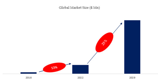
Based on or includes research from QYResearch: Global SiC MOSFET Discrete Market Report 2023-2029.
Market Drivers: electric vehicle (EV) is the largest driver of SiC Power Devices, key applications in EV are Main Inverter (Electric Traction), OBC, and DC-DC.
Global EV sales continued strong. A total of 10,5 million new BEVs and PHEVs were delivered during 2022, an increase of +55 % compared to 2021. China and Europe emerged as the main drivers of strong growth in global EV sales. In 2022, the production and sales of new energy vehicles in China reach 7.0 million and 6.8 million respectively, a year-on-year increase of 96.9% and 93.4%, with a market share of 25.6%. The production and sales of new energy vehicles have ranked first in the world for eight consecutive years. Among them, the sales volume of pure electric vehicles was 5.365 million, a year-on-year increase of 81.6%. In 2022, sales of pure electric vehicles in Europe will increase by 29% year-on-year to 1.58 million.
Figure. SiC MOSFET Discrete, Global Market Size, The Top Five Players Hold 80% of Overall Market
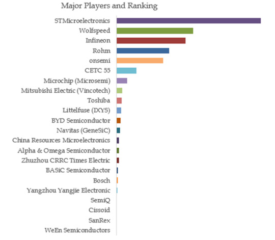
Based on or includes research from QYResearch: Global SiC MOSFET Discrete Market Report 2023-2029.
The key players of SiC MOSFET Discrete are STMicroelectronics, Infineon, Wolfspeed, Rohm, and CETC 55, etc.
About The Authors
Junping Yang - Lead Author
Email: [email protected]
Junping Yang is a technology & market senior analyst specializing in semiconductor devices, materials, and equipment. Yang has 9 years’ experience in semiconductor and focuses on ICs, semiconductor materials, package & testing, power semiconductor (IGBT, SiC, diode, MOSFET, modules and discrete), compound semiconductor (SiC, GaN, etc.), power, RF, optoelectronics, ceramic substrates (HTCC, LTCC, DBC, AMB, DPC, DBA), CMP, equipment & parts (wafer transfer robot, EFEM/Sorter, heaters, etc.). He is engaged in the development of technology and market reports and is also involved in custom projects.
About QYResearch
QYResearch founded in California, USA in 2007.It is a leading global market research and consulting company. With over 16 years’ experience and professional research team in various cities over the world QY Research focuses on management consulting, database and seminar services, IPO consulting, industry chain research and customized research to help our clients in providing non-linear revenue model and make them successful. We are globally recognized for our expansive portfolio of services, good corporate citizenship, and our strong commitment to sustainability. Up to now, we have cooperated with more than 60,000 clients across five continents. Let’s work closely with you and build a bold and better future.
QYResearch is a world-renowned large-scale consulting company. The industry covers various high-tech industry chain market segments, spanning the semiconductor industry chain (semiconductor equipment and parts, semiconductor materials, ICs, Foundry, packaging and testing, discrete devices, sensors, optoelectronic devices), photovoltaic industry chain (equipment, cells, modules, auxiliary material brackets, inverters, power station terminals), new energy automobile industry chain (batteries and materials, auto parts, batteries, motors, electronic control, automotive semiconductors, etc.), communication industry chain (communication system equipment, terminal equipment, electronic components, RF front-end, optical modules, 4G/5G/6G, broadband, IoT, digital economy, AI), advanced materials industry Chain (metal materials, polymer materials, ceramic materials, nano materials, etc.), machinery manufacturing industry chain (CNC machine tools, construction machinery, electrical machinery, 3C automation, industrial robots, lasers, industrial control, drones), food, beverages and pharmaceuticals, medical equipment, agriculture, etc.
0 notes
Text
Semiconductor Manufacturing Equipment Market Surges: A Comprehensive Analysis of the $105.1 Billion Landscape in 2024
The global semiconductor manufacturing equipment market is estimated to be US$ 96.7 billion in 2022 and is expected to reach US$ 105.1 billion by 2023. The global market is predicted to grow at a rate of 7.7% from 2023 to 2033, making it a beneficial investment.
By 2033, it is projected to reach a valuation of US$ 220 billion. This growth is due to the increasing demand for semiconductor manufacturing equipment components, driven by the increase in electronics, automotive, and data processing industries.
Request a Sample Copy of the Semiconductor Manufacturing Equipment Market Report: https://www.futuremarketinsights.com/reports/sample/rep-gb-18089
Semiconductor manufacturing equipment is a vital component of the semiconductor industry, covering chip design, wafer manufacturing, packaging, and testing. It is the driving force behind the development of the semiconductor industry, which produces small electronic devices made from semiconductors such as silicon, germanium, or gallium arsenide compounds. The rapid advancement in manufacturing and increasing acceptance of connected devices among consumers.
The consequent increase in fabrication facilities and the expanding usage of semiconductors in EV manufacturing.
Growing adoption of 5G technology and the rising acceptance of autonomous vehicles.
The worldwide digitalization and the advanced use of electronic devices like laptops, smartphones, and televisions have increased demand for semiconductor manufacturing equipment, particularly in emerging economies. The use of silicon wafers has also improved. Despite contributing significantly to global market growth, budgetary and geopolitical constraints may impact the overall growth rate of the semiconductor manufacturing equipment industry.
Asia Pacific is expected to register the highest CAGR during the forecast period due to the presence of rapidly developing economies, the rising demand for semiconductor manufacturing equipment, the presence of major players in Japan, Taiwan, and China, the increasing need for high-quality processing equipment for semi-conductive materials, and growing government initiatives to support semiconductor industries.
The pandemic has caused supply chain disruptions that may limit the market’s growth to a certain extent. Furthermore, creating user-friendly and easy-to-integrate designs is a challenge for market expansion. Nonetheless, government initiatives to promote the semiconductor industry and the growing use of connected devices in home automation are expected to provide substantial opportunities for market development.
“Rapid growth in automotive and industrial electronics and the proliferation of IoT devices is accelerating the market. Room for the advancement in manufacturing integrated silicon chips for consumer electronics and automobiles is catching the eyes of manufacturers and business leaders.” –opines Sudip Saha, managing director at Future Market Insights (FMI) analyst.
Key Takeaways from the Semiconductor Manufacturing Equipment Market
The global semiconductor manufacturing equipment market is estimated to register a CAGR of 7.7% with a valuation of US$ 220 billion by 2033.
The market captured a CAGR of 9.2% in the historical period between 2018 and 2022.
South Korea is anticipated to dominate the global market by registering a 9.8% CAGR during the forecast period.
With an 8.9% CAGR, the United Kingdom is driving the global market by 2033.
Japan is anticipated to secure a CAGR of 8.8% in the global market during the forecast period.
Key Strategies:
Innovation in electronic devices, automation, and automobiles is attracting manufacturers and industry experts. Over the last few decades, the semiconductor industry has made significant progress, creating smaller, faster, and more reliable devices that have replaced the bulky and hefty vacuum tube technology of the past. Moreover, companies rely on their research and development skills, new materials and techniques, and supply chain management to maintain a competitive advantage.
Recent Developments in the Semiconductor Manufacturing Equipment Market
In 2023, Lam Research India plans to invest US$ 25 million with a US$ 3 million government incentive.
In March 2023, SCREEN PE Solutions Co., Ltd. launched Ledia 7F-L, a direct imaging system designed for high-precision pattern formation on large-sized substrates and metal masks, particularly for telecom and IoT infrastructure.
Leading Key Companies:
Applied Materials Inc.
Lam Research Corporation
KLA Corporation
ASML
Tokyo Electron Limited
Advantest Corporation
SCREEN Holdings Co., Ltd.
Teradyne, Inc.
Hitachi, Ltd.
Plasma-Therm
Seize this Opportunity: Buy Now for a Thorough Report! https://www.futuremarketinsights.com/checkout/18089
Semiconductor Manufacturing Equipment Market Segmentation:
By Equipment Type:
Front-end Equipment
Silicon Wafer Manufacturing
Wafer Processing Equipment
Back-end Equipment
Testing Equipment
Assembling & Packaging Equipment
By Dimension:
2D
2.5D
3D
By Application:
Semiconductor Fabrication Plant/Foundry
Semiconductor Electronics Manufacturing
Test Home
By Region:
North America
Europe
Asia Pacific
Latin America
The Middle East & Africa
0 notes
Text
Fan-out Wafer Level Packaging Market| Analysis and Forecast, 2023 – 2027
Originally published on Technavio: Fan-out Wafer Level Packaging Market by Technology, Type, and Geography - Forecast and Analysis 2023-2027
The Fan-out Wafer Level Packaging (FOWLP) Market is expected to experience significant growth from 2023 to 2027, driven by advancements in semiconductor packaging technologies, the demand for compact and high-performance electronic devices, and the increasing adoption of fan-out packaging solutions. The dynamics of this market are shaped by factors such as the technologies employed in FOWLP, the types of packages offered, and regional trends across the globe.
Fan-out wafer level packaging is an advanced semiconductor packaging technology that involves redistributing the traditional input/output (I/O) pads from the chip's perimeter to an area larger than the chip itself, creating a more space-efficient package. The market encompasses various technologies used in FOWLP, including mold-based fan-out (inFO) and laminate-based fan-out (lFo). inFO technology is known for its high-density packaging and reduced form factor, while lFo technology utilizes organic substrates, providing cost-effective and scalable solutions for semiconductor packaging.
The types of packages within the Fan-out Wafer Level Packaging Market include 2D fan-out packages and 3D fan-out packages. 2D fan-out packages involve redistributing the I/O pads in a two-dimensional plane, offering advantages in terms of size reduction and improved thermal performance. 3D fan-out packages, on the other hand, add an additional dimension by stacking multiple semiconductor dies vertically, providing enhanced performance and functionality in a compact form factor.
Geographically, the market is expected to showcase diverse trends, with North America, Europe, Asia-Pacific, and other regions significantly contributing to market growth. Asia-Pacific, particularly countries like China, Japan, and South Korea, is a key hub for semiconductor manufacturing, driving the demand for advanced packaging technologies such as FOWLP. North America and Europe also play pivotal roles in the market, with a focus on innovation in semiconductor packaging and the presence of leading semiconductor companies.
The forecast period is marked by ongoing innovations in FOWLP technologies, with a focus on improving integration capabilities, increasing the number of I/Os, and enhancing reliability. Manufacturers are exploring new materials, such as advanced mold compounds and organic substrates, to address thermal challenges and optimize the electrical performance of FOWLP solutions. Additionally, the market is witnessing efforts to expand the application scope of FOWLP to address the packaging needs of diverse semiconductor devices.
To Learn deeper into this report , View Sample PDF
Challenges in the Fan-out Wafer Level Packaging Market include addressing the complexity of high-volume manufacturing, ensuring compatibility with various semiconductor processes, and managing the cost considerations associated with advanced packaging technologies. However, the market's growth prospects remain positive as semiconductor manufacturers seek packaging solutions that offer higher integration, improved performance, and a smaller footprint. The industry's evolution is characterized by continuous research and development efforts, collaborations between semiconductor companies and packaging suppliers, and the integration of FOWLP into a broader range of applications, including mobile devices, automotive electronics, and Internet of Things (IoT) devices.
For more information please contact.
0 notes
Text
N-Methyl-2-Pyrrolidone Market: Navigating Challenges and Emerging Victorious

The N-Methyl-2-Pyrrolidone market is estimated to be valued at US$ 1.12 Bn in 2023 and is expected to exhibit a CAGR of 5.8% over the forecast period 2023 to 2030, as highlighted in a new report published by Coherent Market Insights.
Market Overview:
N-Methyl-2-pyrrolidone or NMP is an organic compound that is miscible in both polar and non-polar solvents. It finds wide application as an excellent solvent in industrial cleaning agents, electronics manufacturing, industrial coatings etc. due to its unique solvent properties.
Market Dynamics:
The growth of the N-Methyl-2-Pyrrolidone market is primarily driven by increasing demand from electronics industry. NMP is widely used as a solvent for cleaning semiconductor wafers and electronic components due to its high dielectric constant and miscibility with water as well as organic compounds. It is also used in industrial and architectural coatings applications due to its superior solvency and film forming abilities. Additionally, growing demand for lithium-ion batteries from automotive industry is also supporting the growth of N-Methyl-2-Pyrrolidone market as it is used as electrolyte solvent in lithium-ion battery manufacturing. On the other hand, stringent regulations around the use of NMP due to its toxic nature may hinder the market growth.
SWOT Analysis
Strength: N-Methyl-2-Pyrrolidone has wide range of applications in various end use industries such as electronics, paints & coatings, pharmaceuticals, petrochemicals etc. It acts as an excellent solvent and has high solubility and miscibility. The material has low volatility and good thermal stability.
Weakness: Strict environmental regulations regarding the use and disposal of N-Methyl-2-Pyrrolidone. Extended exposure to NMP can cause skin and eye irritation in humans. High costs associated with the production and manufacturing of NMP.
Opportunity: Growing demand from electronics and lithium-ion battery industries due to increasing usage of NMP as an electrolyte solvent. Rise in paints & coatings industry worldwide is expected to boost the market growth over the forecast period.
Threats: Availability of substitutes such as propylene carbonate and dimethyl sulfoxide may restrict the market growth. Fluctuations in raw material prices can hamper the stability of NMP prices.
Key Takeaways
The global N-Methyl-2-Pyrrolidone market is expected to witness high growth, exhibiting CAGR of 5.8% over the forecast period, due to increasing demand from electronics and lithium-ion battery industries. NMP plays a crucial role as an electrolyte solvent in lithium-ion batteries with high capacity and safety.
Regional analysis: Asia Pacific dominates the global NMP market, with a share of over 35% in 2023. China leads the regional market with the presence of huge electronics and lithium-ion battery industries. Growing demand from end use industries in India and Southeast Asian countries is expected to drive the market growth in the region.
Key players operating in the N-Methyl-2-Pyrrolidone market are BASF SE, LyondellBasell Industries N.V., Ashland Inc., Shandong Qingyun Changxin Chemical Science-Tech Co., Ltd., Hefei TNJ Chemical Industry Co., Ltd., Puyang Guangming Chemicals Co., Ltd., Zhejiang Realsun Chemical Industry Co., Ltd., Abtonsmart Chemical Co. Ltd., and Balaji Amines Limited.
#N-Methyl-2-Pyrrolidone Market Share#N-Methyl-2-Pyrrolidone Market Growth#N-Methyl-2-Pyrrolidone Market Demand#N-Methyl-2-Pyrrolidone Market Trend#N-Methyl-2-Pyrrolidone Market Analysis
0 notes
Text
Electronic Adhesives: The $6.1 Billion Industry Force Powering Modern Electronics

The electronics industry is a rapidly growing sector that relies heavily on a variety of adhesives to ensure the functionality and reliability of electronic devices. These adhesives play a crucial role in bonding components, protecting sensitive circuits, and dissipating heat, making them indispensable for the production of modern electronics.
Market Size and Growth Projections
The global electronic adhesives market is expected to reach a staggering USD 6.1 billion by 2027, expanding at a compound annual growth rate (CAGR) of 6.1% from 2022 to 2027. This impressive growth is fueled by several factors, including:
Rising Demand for Electronic Devices: The increasing demand for smartphones, laptops, wearable devices, and other electronic gadgets is driving the need for high-performance adhesives that can meet the stringent requirements of the electronics industry.
Miniaturization of Electronic Components: As electronic components continue to shrink in size, the need for precision adhesives that can securely bond these tiny components is becoming increasingly important.
Advancements in Adhesive Technologies: Continuous advancements in adhesive technologies are leading to the development of new adhesives with improved properties, such as higher strength, heat resistance, and electrical insulation.
Types of Electronic Adhesives
A wide range of adhesives are utilized in the electronics industry, each with its unique properties and applications:
Epoxies: Epoxies are known for their exceptional strength, durability, and electrical insulation properties, making them ideal for bonding semiconductors, capacitors, and other electronic components.
Acrylics: Acrylics offer versatility and ease of application, making them suitable for bonding flexible printed circuits and other applications where flexibility is crucial.
Silicones: Silicones provide superior resistance to heat, chemicals, and vibration, making them excellent choices for sealing applications, protecting electronic components from environmental hazards.
Polyurethanes: Polyurethanes exhibit strong adhesion and remarkable bonding strength to a variety of substrates, making them suitable for bonding metal and plastic components in electronic devices.
Application Segments of Electronic Adhesives
The electronic adhesives market is segmented into various applications, each with its distinct growth drivers:
Semiconductor Manufacturing: The semiconductor industry is a major consumer of electronic adhesives, with adhesives used in wafer bonding, encapsulation, and device packaging.
Printed Circuit Board (PCB) Assembly: PCBs are the backbone of modern electronics, and adhesives play a critical role in bonding components, securing traces, and providing electrical insulation.
Consumer Electronics: Smartphones, laptops, tablets, and other consumer electronics devices rely heavily on adhesives for assembly, sealing, and heat dissipation.
Automotive Electronics: The increasing complexity of automotive electronics is driving the demand for high-performance adhesives that can withstand harsh automotive environments.
Medical Electronics: Medical devices require adhesives that meet stringent regulatory standards and offer biocompatibility with human tissues.
Geographical Landscape of the Electronic Adhesives Market
The global electronic adhesives market is dominated by Asia Pacific, primarily driven by the strong electronics manufacturing industry in China, South Korea, and Taiwan. North America and Europe also hold significant market shares due to their advanced technological expertise and established electronics manufacturing bases.
Key Players in the Electronic Adhesives Market
The electronic adhesives market is characterized by a competitive landscape, with several major players vying for market share:
Henkel AG & Co. KGaA
3M
H.B. Fuller Company
Dow Chemical Company
Huntsman Corporation
Eastman Chemical Company
Avery Dennison Corporation
Nitta Corporation
tesa SE
Würth Group
Download PDF Brochure :
The electronic adhesives market is poised for robust growth in the coming years, driven by the increasing demand for electronic devices, advancements in adhesive technologies, and the expansion of the electronics industry into new applications. As electronic devices become more complex and sophisticated, the role of electronic adhesives will become even more critical in ensuring the performance, reliability, and durability of these devices.
0 notes
Text
Semiconductor Packaging Market Size Growth Of $60.44 Billion by 2030
According to a new report published by Allied Market Research, titled, “Semiconductor Packaging Market by Type, Packaging Material, Wafer Material, Technology, and Industry Vertical: Global Opportunity Analysis and Industry Forecast, 2021–2030” the global semiconductor packaging market size was valued at $27.10 billion in 2020 and is projected to reach $60.44 billion by 2030, registering a CAGR of 9.10% during the forecast period. Asia-Pacific is expected to be the leading contributor to the global market, followed by North America and Europe.
Semiconductor packaging is an advanced semiconductor packaging technology where the layers of components inside and integrated circuit (IC) are stacked together while the horizontal and vertical connections are made to keep them in place and work as a single device. Semiconductor packaging offers distinct advantages over other packaging technologies such as reduced power consumption, enhanced efficiency, better overall performance, and high frequency of operation.
Download Research Report Sample & TOC: Semiconductor Packaging Market Forecast, 2021–2030

Emerging technologies, such as artificial intelligence (AI) and quantum computing, require compound semiconductors to achieve full commercialization. The UK has a rich heritage of microprocessor design, with companies, such as ARM and Imagination Technologies, and new start-up companies designing AI processors, such as Bristol-based GraphCore, which are expected to create lucrative opportunities for the global semiconductor packaging market growth.
China is the largest country, in terms of revenue generation, in the global semiconductor packaging market share. The semiconductor packaging industry is well-established in China and Taiwan. In addition, rapid growth in sales of consumer electronic products supplements the market growth. Moreover, increase in defense expenditure and widespread use of semiconductors material in IT & telecommunication, consumer electronics, and automotive industries drive the growth of the semiconductor packaging market revenue. Increase in demand for high-speed and compact size electronic products boosts the adoption of flip chip technology in the electronic industry. Internet of Things (IoT) has been gaining popularity and serves as a key driver of the market.
Products used in IoT, such as sensors & actuators, analog & mixed-signal translators, and microcontrollers or embedded processors, require efficient and reliable packaging solutions, which can be done using flip chips, contributed the highest share in the global semiconductor packaging market. In comparison to customary wire-bond packaging, flip chip offers various benefits such as superior thermal & electrical performance, substrate flexibility for varying performance requirements, remarkable I/O capability, reduced form factors, and well-established process equipment expertise.
By region, the semiconductor packaging market trends have been analyzed across North America, Europe, Asia-Pacific, and LAMEA. The market analysis had identified that Asia-Pacific contributed maximum revenue in 2020 and is expected to grow at a faster rate as compared to other regions.
Inquiry Before Buying: Semiconductor Packaging Market
Covid 19 Impact Analysis
The impact of COVID-19 on the manufacturing industry has significantly affected the global economy. Electronic components, such as PCBs, LED chips and wafers, ICs, and other semiconductor devices, are mostly imported from China. Attributed to the shutdown of manufacturing units, the prices of semiconductor components have increased by 2-3%, owing to shortage of supplies.
The ongoing COVID-19 pandemic has abruptly re-shaped the global economy. Sudden decline in infrastructure development and installation projects is expected to hamper the semiconductor packaging market growth for automotive and other industrial verticals.
Key Findings Of The Study
In 2020, the flip chip segment accounted for maximum revenue and is projected to grow at a notable CAGR of 8.40% during the forecast period.
The consumer electronics segment accounted for more than 45% of the semiconductor packaging market share in 2020.
The fan-out WLP segment is expected to witness the highest growth rate during the forecast period.
UK was the major shareholder in the Europe semiconductor packaging market, accounting for approximately 35% share in 2020.
The key players profiled in the report include Amkor Technology (U.S.), ASE Group (Taiwan), ChipMOS Technologies, Inc. (Taiwan), Powertech Technology, Inc. (Taiwan), Intel Corporation (U.S.), Jiangsu Changjiang Electronics Technology Co., LTD (China), Samsung Electronics Co., Ltd. (South Korea), Taiwan Semiconductor Manufacturing Company (Taiwan), Texas Instruments (U.S.), and Fujitsu Limited (Japan). Market players have adopted various strategies, such as product launch, collaboration, product development, agreement, and expansion, to expand their foothold in the semiconductor packaging industry.
About Us:
Allied Market Research is a top provider of market intelligence that offers reports from leading technology publishers. Our in-depth market assessments in our research reports take into account significant technological advancements in the sector. In addition to other areas of expertise, AMR focuses on the analysis of high-tech systems and advanced production systems. We have a team of experts who compile thorough research reports and actively advise leading businesses to enhance their current procedures. Our experts have a wealth of knowledge on the topics they cover. Also, they use a variety of tools and techniques when gathering and analyzing data, including patented data sources.
Contact Us:
David Correa
1209 Orange Street
Corporation Trust Center
Wilmington
New Castle
Delaware 19801
USA Int'l: +1-503-894-6022
Toll Free: +1-800-792-5285
Fax: +1-800-792-5285
0 notes
Text
Thin Wafer Market Share, Size, Trends & Growth Drivers – 2026
The thin wafer market is projected to grow from USD 11.4 billion in 2022 to reach USD 20.6 billion by 2027; it is expected to grow at a Compound Annual Growth Rate (CAGR) of 12.5% from 2022 to 2027.
Rising adoption of MEMS technology in portable health monitoring devices, reducing sizes of electronic devices, growing smartphone and consumer electronics markets and high amount of material saving is expected to fuel the growth of the thin wafer industry.
Thin wafer market for CIS applications is expected to grow at a significant CAGR during the forecast period.”
The thin wafer market for CIS application is expected to grow at a significant CAGR during the forecast period. CIS is used in mobile phones and other consumer electronic devices. The miniaturization of these electronic devices generates the need for thick and thin CMOS chips. Hence, to develop thin CIS chips, thin wafers are used during their fabrication. This has led to an increased demand for CIS thereby paving way for the growth of thin wafer market.
Wafer dicing equipment to hold the largest market share of the thin wafer market during the forecast period”
Wafer dicing dominated the thin wafer market in 2021 and is expected to follow the trend during forecast period. An increase in memory capacity and continuous package miniaturization require ultra-thin wafer dicing. In recent years, there has been an increasing adoption of RFID tags and SIP (system in package) for smartphones and other compact electronic devices. This has resulted in the rapid growth of finished semiconductor die with thickness less than or equal to 100 µm. This growing demand has made the processing of thin wafers an essential competence for many integrated device manufacturers. The increasing demand for high-speed dicing combined with superior breakage strength has paved way for an increased demand for the wafer dicing equipment.
Download PDF Brochure: https://www.marketsandmarkets.com/pdfdownloadNew.asp?id=255706993
Thin wafer market in Asia Pacific estimated to grow at the fastest rate during the forecast period
Asia Pacific plays a pivotal role in the development of the electrical and electronics industry. A few of the leading thin wafer manufacturing companies such as Shin-Etsu Chemical Co., Ltd. (Japan), SUMCO Corporation (Japan), GlobalWafers Co., Ltd. (Taiwan), DISCO Corporation (Japan) are based in Asia Pacific. The high growth of Asia Pacific can be attributed to the surging adoption of high-end consumer electronics, such as wearables and smart home devices in China and Japan. The global semiconductor market is expected to unveil substantial development in the Asia Pacific region due to favorable economic conditions and increasing demand for consumer electronics. As Asia Pacific has low labor cost most of the thin wafers and wafer thinning equipment are manufactured in Asia Pacific and are exported to various regions. The significant growth toward manufacturing and the potential of China, Japan, and Taiwan are largely contributing to this growth trend.
About MarketsandMarkets™
MarketsandMarkets™ is a blue ocean alternative in growth consulting and program management, leveraging a man-machine offering to drive supernormal growth for progressive organizations in the B2B space. We have the widest lens on emerging technologies, making us proficient in co-creating supernormal growth for clients.
The B2B economy is witnessing the emergence of $25 trillion of new revenue streams that are substituting existing revenue streams in this decade alone. We work with clients on growth programs, helping them monetize this $25 trillion opportunity through our service lines - TAM Expansion, Go-to-Market (GTM) Strategy to Execution, Market Share Gain, Account Enablement, and Thought Leadership Marketing.
Built on the 'GIVE Growth' principle, we work with several Forbes Global 2000 B2B companies - helping them stay relevant in a disruptive ecosystem.Our insights and strategies are molded by our industry experts, cutting-edge AI-powered Market Intelligence Cloud, and years of research.The KnowledgeStore™ (our Market Intelligence Cloud) integrates our research, facilitates an analysis of interconnections through a set of applications, helping clients look at the entire ecosystem and understand the revenue shifts happening in their industry. To find out more, visit www.MarketsandMarkets™.com or follow us on Twitter, LinkedIn and Facebook.
0 notes
Text
The Photoresist Ancillaries Market is projected to witness substantial growth, with the market value expected to surge from USD 4,125.63 million in 2023 to reach USD 6,455.27 million by 2032, reflecting a notable compound annual growth rate (CAGR) of 5.10% during the forecast period.The photoresist ancillaries market plays a crucial role in the semiconductor and electronics industries, providing essential materials that support the manufacturing processes of integrated circuits (ICs), printed circuit boards (PCBs), and other electronic components. These ancillaries are integral to the photolithography process, which is foundational to creating intricate patterns on semiconductor wafers and other substrates.
Browse the full report at https://www.credenceresearch.com/report/photoresist-ancillaries-market
Market Overview
The global photoresist ancillaries market has witnessed steady growth in recent years, driven by advancements in semiconductor technology and the increasing demand for smaller, more efficient electronic devices. Photoresist ancillaries encompass a range of materials and chemicals, including developers, removers, primers, and edge-bead removers, among others. These materials are designed to enhance the performance and efficiency of photoresist materials used in photolithography processes.
Key Drivers of Market Growth
Several factors contribute to the growth of the photoresist ancillaries market:
1. Technological Advancements: Continuous innovations in semiconductor manufacturing technology, such as the development of advanced photoresists and ancillary materials, drive the demand for high-performance ancillary products.
2. Increasing Demand for Electronics: The proliferation of electronic devices across various sectors, including consumer electronics, automotive, and telecommunications, fuels the demand for advanced semiconductor components, thereby boosting the market for photoresist ancillaries.
3. Miniaturization Trends: The trend towards smaller and more complex electronic devices requires finer patterning capabilities, which in turn necessitates high-quality photoresist ancillaries for precise lithographic processes.
4. Geographical Expansion: Emerging economies in Asia-Pacific, particularly China, Japan, and South Korea, are significant contributors to market growth due to their expanding semiconductor and electronics manufacturing sectors.
Challenges and Opportunities
Despite robust growth prospects, the photoresist ancillaries market faces challenges such as stringent environmental regulations and volatility in raw material prices. Manufacturers are increasingly focusing on developing eco-friendly ancillary solutions and optimizing production processes to mitigate these challenges.
Opportunities abound for market players to capitalize on:
1. Research and Development: Investment in research and development to innovate new ancillary products that meet evolving technological requirements and regulatory standards.
2. Collaborations and Partnerships: Strategic collaborations between semiconductor manufacturers, research institutions, and ancillary suppliers can foster innovation and accelerate market penetration.
3. Market Expansion: Exploring untapped markets in emerging economies and diversifying product portfolios to cater to a wide range of applications in the electronics industry.
Future Outlook
The future of the photoresist ancillaries market looks promising with anticipated advancements in semiconductor technology and the growing adoption of advanced electronic devices worldwide. Continued investments in research and development, coupled with strategic initiatives to address environmental concerns, are expected to drive sustainable growth in the market.
Key Players
Tokyo Ohka Kogyo Co., Ltd.
JSR Corporation
Merck KGaA
Shin-Etsu Chemical Co., Ltd.
Dow Inc.
Fujifilm Holdings Corporation
MicroChem Corporation
Avantor, Inc.
DuPont de Nemours, Inc.
Sumitomo Chemical Co., Ltd.
Segments:
By Types:
Anti-reflective Coatings
Photoresist Developers
Edge Bead Removers
Other Type
By Application:
Semiconductors and Integrated Circuits
Printed Circuit Boards
Other Application
By Region
North America
Europe
Japan
Latin America
The Middle East and Africa
Asia-Pacific
About Us:
Credence Research is committed to employee well-being and productivity. Following the COVID-19 pandemic, we have implemented a permanent work-from-home policy for all employees.
Contact:
Credence Research
Please contact us at +91 6232 49 3207
Email: [email protected]
0 notes
Text
Elemental Fluorine Market Industry report covers the increasing demand by top players

Elemental fluorine is a highly reactive, pale yellow-green gas that is part of the halogen group on the periodic table. It is the most electronegative and reactive of all elements, and as a result, it does not occur naturally in its elemental form. Instead, fluorine is typically found in combination with other elements, such as in the mineral fluorspar (calcium fluoride) or in the compound hydrofluoric acid (HF).
Fluorine is used in a variety of industries, including the production of chemicals, plastics, and metals. It is also used in the pharmaceutical industry to produce drugs such as fluoxetine (Prozac) and enflurane (Ethrane). Other applications of elemental fluorine include the manufacturing of semiconductors, rocket fuel, and nuclear fuels.
The global elemental fluorine market is projected to grow significantly in the coming years, driven by increasing demand from the chemical and semiconductor industries. The global elemental fluorine market size was valued at USD 23.5 million in 2020 and is expected to reach USD 29.9 million by 2025, growing at a CAGR of 4.9% during the forecast period.
One of the key drivers of the market is the growing demand for fluoropolymers, which are used in a wide range of applications including coatings, films, and membranes. These materials have excellent chemical resistance, high temperature resistance, and non-stick properties, making them ideal for use in harsh environments. The semiconductor industry is also a major consumer of elemental fluorine, as it is used in the production of silicon wafers and other semiconductor materials.
North America and Asia-Pacific are the two largest markets for elemental fluorine, accounting for a significant share of the global demand. The Asia-Pacific region is expected to be the fastest-growing market, driven by the increasing demand from the chemical and semiconductor industries in countries such as China, India, and Japan.
However, the market growth may be hindered by factors such as the high cost of production and the stringent regulations regarding the use and handling of elemental fluorine due to its highly reactive nature and potential health hazards. Nevertheless, ongoing research and development of new applications and production methods for elemental fluorine are expected to drive the market growth in the long term.
0 notes
Text
SEMI predicts that the global 300mm fab production capacity will hit a new high in 2026

Recently, the International #semiconductor Industry Association (SEMI) released a new report, predicting that the global 300mm fab production capacity will increase to 9.6 million wafers per month (WPM) in 2026, which will hit a record high, and the share of mainland China will surpass that of South Korea. After strong growth in 2021 and 2022, the expansion of 300mm capacity will slow down this year due to weak demand for memory and logic devices.
According to Ajit Manocha, President and CEO of SEMI, Lansheng Technology Limited believes that although the capacity expansion of 300mm fabs around the world is slowing down, the industry is still focused on increasing capacity to meet the strong long-term demand for semiconductors. SEMI expects that between 2022 and 2026, #tsmc , Samsung, #umc , #globalfoundries , #smic , #HuaHongSemiconductor, Intel, SK Hynix, #kioxia , Micron, STMicroelectronics and Texas Instruments will all Increased capacity for 300mm wafers, with a total of 82 new facilities and production lines in operation.
Mainland China will focus on mature process nodes, and its global share will increase from 22% in 2022 to 25% in 2026. The production capacity of 300mm fabs will reach 2.4 million pieces per month; The share of round factory capacity will drop from 25% in 2022 to 23% in 2026; Taiwan will continue to maintain its third position, but its share will drop slightly, from 22% in 2022 to 21% in 2026; Japan’s share of 300mm fab capacity is also expected to decline, from 13% in 2022 to 12% in 2026, mainly related to increased competition in other regions.
Driven by government-led investment and strong demand in the automotive sector, the share of 300mm fab capacity in the Americas, Europe and the Middle East will increase between 2022 and 2026, with the Americas rising 0.2% to 9 %; the share of Europe and the Middle East will increase from 6% to 7%; the share of Southeast Asia will remain at 4%.
According to SEMI, capacity growth in the analog and power sectors will lead other sectors, with a compound annual growth rate (CAGR) of 30%, followed by foundry (12%), optoelectronics (6%) and memory (4%) . SEMI lists a total of 366 facilities and production lines, of which 258 are in operation and 108 are planned for construction.
Lansheng Technology Limited (https://www.lanshengic.com) is a global distributor of electronic components that has been established for more than 10 years, headquartered in Shenzhen China, who mainly focuses on electronic spot stocks.
0 notes
Text
Silicon Wafer Reclaim Market Surge to Witness Huge Demand at a CAGR of 17.05% during the forecast period 2028
Industry Analysis
Silicon wafer reclaim market size is valued at USD 2,353.94 million by 2028 is expected to grow at a compound annual growth rate of 17.05% in the forecast period of 2021 to 2028. Data Bridge Market Research report on silicon wafer reclaim provides analysis and insights regarding the various factors expected to be prevalent throughout the forecasted period while providing their impacts on the market’s growth.
Additionally, the credible Silicon Wafer Reclaim Market report helps the manufacturer in finding out the effectiveness of the existing channels of distribution, advertising programs, or media, selling methods and the best way of distributing the goods to the eventual consumers. Taking up such market research report is all the time beneficial for any company whether it is a small scale or large scale, for marketing of products or services. It makes effortless for Semiconductors and Electronics industry to visualize what is already available in the market, what market anticipates, the competitive environment, and what should be done to surpass the competitor.
Get a Free Sample of The Report: https://www.databridgemarketresearch.com/request-a-sample/?dbmr=global-silicon-wafer-reclaim-market
Market Insights and Scope
Silicon wafer reclaim is a type of multi-step procedure which transforms a used wafer with numerous layers of various materials into a qualification wafer. The major steps integrated in wafer reclaim are sorting, stripping, lapping and grinding, polishing, cleaning and the inspection.
The Silicon Wafer Reclaim Market report encompasses various segments linked to Semiconductors and Electronics industry and market with comprehensive research and analysis. These comprise industry outlook with respect to critical success factors (CSFs), industry dynamics that mainly covers drivers and restraints, market segmentation & value chain analysis, key opportunities, application and technology outlook, regional or geographical insight, country-level analysis, key company profiles, competitive landscape, and company market share analysis. All the data, figures and information are backed up by well recognized analysis tools which include SWOT analysis and Porter’s Five Forces analysis. So, take business to the peak level of growth with the all-inclusive Data Bridge Market research report.
Get full access to the report: https://www.databridgemarketresearch.com/reports/global-silicon-wafer-reclaim-market
Industry Segmentation and Size
Silicon wafer reclaim market is segmented on the basis of reclaim capacity, application and end user. The growth among segments helps you analyze niche pockets of growth and strategies to approach the market and determine your core application areas and the difference in your target markets.
On the basis of reclaim capacity, the silicon wafer reclaim market is segmented into 150 mm, 200 mm, 300 mm and >300 mm.
The application segment of the silicon wafer reclaim market is segmented into integrated circuits, solar cells, photoelectric cells and others.
Based on end user, the silicon wafer reclaim market is segmented into automotive, aerospace and defense, mining and construction, electronics and others. Others have further been segmented into medical and sports.
Market Country Level Analysis
The countries covered in the silicon wafer reclaim market report are
U.S., Canada and Mexico in North America, Brazil, Argentina and Rest of South America as part of South America, Germany, Italy, U.K., France, Spain, Netherlands, Belgium, Switzerland, Turkey, Russia, Rest of Europe in Europe, Japan, China, India, South Korea, Australia, Singapore, Malaysia, Thailand, Indonesia, Philippines, Rest of Asia-Pacific (APAC) in the Asia-Pacific (APAC), Saudi Arabia, U.A.E, South Africa, Egypt, Israel, Rest of Middle East and Africa (MEA)as a part of Middle East and Africa (MEA).
A reliable Silicon Wafer Reclaim Market marketing report proves to be the finest and excellent market research report as it is formulated with the following critical factors. These consist of primary research, benchmarking studies, secondary research, company profiles, competitive intelligence & reporting, syndicated research, data collection, data processing and analysis, survey design, and survey programming. The report performs market study and analysis to provide market data by considering new product development from beginning to launch. The Semiconductors and Electronics business report also provides evaluations based on the market type, organization size, availability on-premises, end-users’ organization type, and the availability in areas such as North America, South America, Europe, Asia-Pacific and Middle East & Africa.
Industry Share Analysis
The major players covered in the silicon wafer reclaim market report are
NanoSILICON, Inc., AnySilicon, Pure Wafer, Silicon Valley Microelectronics, Inc., Noel Technologies, Inc., RS Technologies Co., Ltd., Phoenix Silicon International Corporation, Polishing Corporation of America, Naura-Akrion, Optim Wafer Services, KINIK COMPANY, Silicon Specialist LLC, Global Silicon Technologies, Nippon Chemi-Con Corporation, DSK Technologies Pte Ltd., and MicroSil, LLC among other domestic and global players. Market share data is available for global, North America, Europe, Asia-Pacific (APAC), Middle East and Africa (MEA) and South America separately.
Browse Related Reports@
Global Whiskey Market
South Africa Battery Market
Global Plant-Based Egg Market
Global Nutritional Beverages market
MENA Tahini market
Global Dental Membrane and Bone Graft Substitute Market
About Us:
Data Bridge Market Research set forth itself as an unconventional and neoteric Market research and consulting firm with an unparalleled level of resilience and integrated approaches. We are determined to unearth the best market opportunities and foster efficient information for your business to thrive in the market
Contact:
Data Bridge Market Research
Tel: +1-888-387-2818
Email: [email protected]
#Silicon Wafer Reclaim Market Growing Popularity#Silicon Wafer Reclaim Market Global Leading Brands#Silicon Wafer Reclaim Market drivers-advantages#Silicon Wafer Reclaim Market Segmentation-CAGR rate#Silicon Wafer Reclaim Market Demands-Size-Share-Top Trends#Silicon Wafer Reclaim Market Industry-Competitors#Silicon Wafer Reclaim Market Growth-Competition#Silicon Wafer Reclaim Market 2028 by Types-Application#Silicon Wafer Reclaim Market Semiconductors and Electronics Industry
0 notes
Last Seen Blogs

letshardcollectorstudent-blog
Untitled

theeyoungalabastor
TheeYoungAlabastor

coleydp
Coley

orujov
Orujov

dynamicsimp
Puppit Lurker