#Microelectronics
Explore tagged Tumblr posts
Visit Tumblr Blog
Explore Tumblr blogs with no restrictions, modern design and the best experience.
Last Seen Tumblr Blogs


Fun Fact
Users from the US are the majority of Tumblr visitors.
Text
MOAR Sparkle Motion testing - built-in I2S mic 🎤📊
We're rounding the corner with testing our Sparkle Motion
WLED-compatible board. We're doing the audio-reactive test with the built-in I2S microphone this time. This digital mic will give great audio quality without needing any extra work. If you want an external mic wired far away, there are GPIOs exposed that you can solder to for another I2S connection - ESP32 lets you use any pins, which is nice! this demo is a graphical equalizer that makes verification easy! All we have left is to test the IR remote and fuse, and we're good to go!
#sparklemotion#i2smicrophone#wled#esp32#audioreactive#graphicalequalizer#digitalaudio#electronicsdiy#techinnovation#adafruit#makersmovement#microcontrollers#embeddeddesign#audioquality#irremote#fuse#gpio#iotdevices#hardwaretesting#electronicsengineering#soldering#digitaltech#audioenthusiast#openhardware#techdemos#gadgettesting#techprojects#microelectronics#techmaker#innovativetech
11 notes
·
View notes
Text
getting a raspberry pi pico for a project 💪🏼 it's gonna be fun
2 notes
·
View notes
Text

Probe Card
Wentworth Laboratories
19 notes
·
View notes
Text


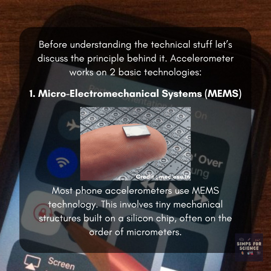


How does your phone 📲 know you turned into a landscape artist?👩🏻🎨 Can you outsmart its rotation sense? We notice this happen several times a day, sometimes wonder🤔 about the how and then let it just slip from the mind within a few seconds. Swipe through this post to unfold 📖the tech behind this magic trick !🪄🎩
#accelerometer#microelectronics#technology#techgeek#tech#phone#engineering#physics#devices#electronics#education#science#science facts#study blog#discover#scicomm#research scientist#explore#smartphone#smartwatch#capacitors#cool science#simps for science
11 notes
·
View notes
Text
I SAW THE FACE OF GOD IN A SILICON WAFER
2 notes
·
View notes
Text

Wow, didn't expect this unique answer.
Wanna try? @productofaritual @a-sociopath-do-your-research @hydehydejeykll @starlyte-writes @globlingoober
Would you like to find out what you would be the god of? Take my new uqiz to find out
#lil something#writing#uquiz#have fun with it please#assigning the 30+ results was fucking exhausting#you can get#spins wheel#mascots#emojis#longing#microelectronics#and so many more!#quiz#tag game#etc#mine#callisteios#i will add more answers. when I have inspiration and or energy#muted
66K notes
·
View notes
Text
#EngineeringExcellence#Microelectronics#Innovation#TechTalent#HKSTP#WürthElektronik#AdvancedManufacturing#SmartCity#StartupSupport#IndustryCollaboration#powerelectronics#powermanagement#powersemiconductor
0 notes
Text
At Intel Foundry Event, Secures Government Microelectronics

Event Intel Foundry
Intel is committed to defending the domestic chip supply chain and reclaiming semiconductor dominance as the sole American semiconductor developer and manufacturer. Working with the U.S. government, Intel seeks to boost U.S. technological systems with creative, secure solutions.
The State-of-the-Art Heterogeneous Integration Prototype (SHIP) and Rapid Assured Microelectronics Prototypes-Commercial (RAMP-C) with the U.S. Department of Defence (DoD) have accelerated the development of advanced semiconductor technologies and demonstrate how public and commercial interests can collaborate to innovate and improve national security.
Intel's devotion and Intel Foundry's vital role have led to amazing advancements.
Industry-leading Intel 18A process technology enters risk production
The cutting-edge Intel 18A process node from Intel Foundry has transformed defence. For the first time in decades, USG and DIB clients may use cutting-edge technology alongside commercial customers. DIB clients adopting Intel 18A technology for their latest microelectronics and mission platforms will enhance military SWaP-C requirements.
According to Intel Foundry SVP and GM Kevin O'Buckley, the final Intel 18A PDK 1.0.1GA was released in Q4 2024, and Intel 18A technology is in risk production.
Building Intel 18A ITAR-compliant test chip support
One of the more intriguing IPSS announcements was allowing ITAR access to Intel 18A test chips. This ensures DIB clients may employ cutting-edge technology while meeting program requirements. For early 2026 tape-outs, the Intel 18A ITAR test chip shuttle is accepting reservations.
Adding 12nm to Foundry's roadmap
For clients who need onshore access to established technologies, Intel Foundry will provide 12nm process technology in 2026. This FinFET-based technology will be built in Arizona. DIB clients can create tape-outs in late 2026.
Onshore advanced packaging scaling
In order to address mission system requirements, Intel Foundry offers its cutting-edge heterogeneous packaging technologies, including as Foveros 3D, EMIB 3.5D, and EMIB, onshore. Chiplet libraries and advanced semiconductor packaging help customers quickly conceive, develop, build, test, and integrate cutting-edge devices into field equipment. For autonomous systems and secure communications, Intel cutting-edge packaging technologies provide the performance and security needed for mission-critical operations and enable the latest military technology to be available in sophisticated system-level packaging for SHIP.
Adding Secure Enclave and DIB customers to USG cooperation
Intel won the Secure Enclave (SE) program last year, building on its programmatic engagement in SHIP and RAMP-C. SE aims to boost the U.S. government's dependable manufacture of cutting-edge semiconductors.
Intel Foundry added Reliable MicroSystems and Trusted Semiconductor Solutions to its DIB client list earlier this year as part of RAMP-C's third phase. Intel Foundry's cutting-edge Intel 18A process technology and advanced packaging for high-volume manufacture and prototypes will benefit more DIB clients with their integration.
Ready to Serve: Intel Foundry
The Intel Foundry can meet government application needs. Due to its cutting-edge Intel 18A process technology, advanced packaging choices, and safe manufacturing, Intel Foundry can deliver high-performance, reliable, and secure semiconductor products. Intel Foundry may be a trusted partner in developing microelectronics for critical government applications using SOTA technology and close collaboration with the USG and DoD.
Intel Foundry Direct Connect
Attend Intel Foundry Direct Connect, the premier annual event in San Jose, California, on April 29, 2025, to network with government, defence, and aerospace experts. Connect with clients, defence industry experts, and USMAG alliance ecosystem partners to learn how process technology, cutting-edge packaging, and testing may support your ideas. At 9 a.m. PDT, CEO Lip-Bu Tan will start the event. Join today to learn about future systems foundry design and production.
Intel technology may need hardware, software, or service activation. No part or product is absolutely safe. Your costs and results vary.
#technology#technews#govindhtech#news#technologynews#Intel Foundry Event#Intel Foundry#Intel 18A process technology#Intel 18A#Intel Foundry Direct Connect#Microelectronics
0 notes
Text

The Science Research Notebooks of S. Sunkavally, p 784.
#monoamines#lithium carbonate#brain#nitrous acid#head injury#combat#collagen#hypothermia#phenols#drosophila#microelectronics#transistors#heat dissipation#atomic orbitals#thyroid hormone#oxidative uncoupling#neuron activity#thermogenesis#molecular electronics#nitroamine benzenethiol#benzene ring
1 note
·
View note
Text
Job - Alert 📢

🚀 Join Our Team! 🌍
Silicon Austria Labs is looking for an Expert - Business Development (all genders) in Villach!
🆔 Job-ID: 167-1
🗓️ Full-time, Permanent Position
As part of our dynamic Business Development team, you will drive strategic growth in our Sensor Systems division, develop new markets, and represent SAL at national and international events. If you have a passion for innovation and a strong background in electronics or engineering, we want to hear from you!
👉 Apply now and help us shape the future of technology: https://www.academiceurope.com/job/?id=6313
#hiring#jobs#science#jobseekers#electronics#electronicsengineering#electricalengineering#microelectronics#physics#sensors
0 notes
Text
Chikken Chekkinator
I've been working on a thing for the past few weeks to keep track of chicken chores so we dont have to ask "have you fed the chickens" all the time

Its not finished, i need to get the final art printed but i'm pretty happy with it so far. It lights up different colours depending on who did the task, it gets saved to home assistant so you can view the status remotely and get reminders, and it changes its brightness based on the time of day so its not too bright at night.
i learned so much about microprocessor programming doing this and had a lot of fun. I think i want to make more things like this for helping my ADHD brain do regular tasks
here's the (almost) final artwork that i need to print for it:

i might do a technical writeup of how it works if people are interested
#microelectronics#diy project#esp8266#oc#going to post about some projects im working on because a shitpost i made broke containment and im gonna use that as motivation
8 notes
·
View notes
Text
Microelectronics Commons: $160M Investment by U.S. DoD.
Microelectronics Commons: $160M Investment by U.S. DoD. In a significant move to bolster America’s technological edge, the U.S. Department of Defense has announced an additional investment of $160 million in microelectronics through the CHIPS and Science Act. This funding aims to advance the nation’s microelectronics capabilities by supporting the Microelectronics Commons, a collaborative…
0 notes
Text

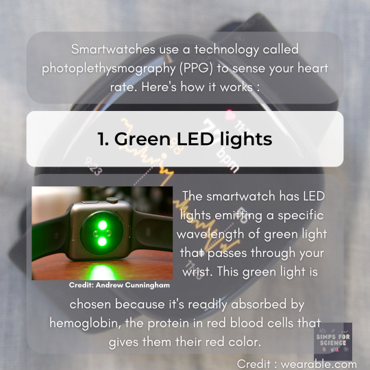


🤔 Ever wondered how could your smartwatch be your heart's 🫀 personal translator and track every beat? It's not magic, 🪄🔮 it's all about pretty cool Science 🔎 wrapped around tiny tech detectives, light, and blood flow! Swipe ➡️ through this post to uncover the tech behind this.
#education#science#science facts#discover#study blog#scicomm#research scientist#explore#physics#physicist#tech#technology#tech geek#techgeek#microelectronics#smartwatch#smart devices#devices#electronics#electronic#semiconductor#processor#green#green light#scientist#scifi#cool science
8 notes
·
View notes
Text
Connect STM32C0 to computer
Notes to self because I'm sure I'll forget this in three months time.
STLink v2 (generic cheap clone) doesn't seem to work (or I'm being stupid)
STLink v3 MINIE is the weapon of choice
Does not have any useful plugs whatsoever but you can solder wires to the edge connector fingers at the bottom
That feels wrong but honestly when am I going to design a board that's gonna need those? My stuff is for model railroads I don't have space for an edge connector like that
TMS to SWDIO
CLK to SWCLK
RST to NRST (no special logic necessary, yes even though NRST is negated, it seems they didn't have space for that extra letter on the board). This is optional according to ST, and in my case the cable came off and everything still worked, so, you know
GND to GND
VCC to your target 3.3V output! The thing you have on your board to power your MCU. STLink v3 MINIE uses this only to find out what you're running the MCU at. Implied in this: You can't use this STLink to power your target board, you always have to provide external power.
Most important letter in STLink is the L.
It's really not that difficult once you've figured this all out, and thankfully I had ordered this STLink v3 on a whim earlier, but it's not directly apparent. I'm sure there's an application note or something that will tell you this even better.
#programming#microelectronics#electronics#mcu#stm32#stlink#stm32c0#STM32C031C4#STM32C031C4G6#say what you want but 48 MHz for the price of an ATTiny?#I don't even need 48 MHz for my model railroad train car lighting but if I can get it I mean why not
1 note
·
View note
Text
Epitaxial Wafer Market Trends Growth by Innovation in LED lighting
The epitaxial wafer market plays a pivotal role in manufacturing high-performance semiconductor devices used in applications ranging from consumer electronics to advanced healthcare devices. Epitaxial wafers aid in developing sophisticated integrated circuits and semiconductor chips through epitaxial growth techniques. Advancements in LED technology have increased the demand for epitaxial wafers for commercial and industrial applications. The global epitaxial wafer market is expected to gain significant traction on account of rising adoption of LED lighting and displays.
The Epitaxial Wafer Market size was valued at USD 2,778 million in 2022 and is anticipated to witness a compound annual growth rate (CAGR) of 12.9% from 2022 to 2030.
Key players operating in the epitaxial wafer market are EpiWorks Inc., Global Wafers Japan Co. Ltd., Nichia Corporation, SHOWA DENKO K.K., Siltronic AG, Desert Silicon Inc., Electronics and Materials Corporation Ltd. Intelligent Epitaxy Technology Inc.IQE plc., Jenoptic AG, MOSPEC Semiconductor Corporation, Norstel AB, Ommic S.A., Silicon Valley Microelectronics Inc., SVT Associates Inc. Universal Wafer Inc., Wafer Works Corporation, Xiamen Powerway Advanced Materials Co. Ltd., and Visual Photonics Epitaxy Co. Ltd. Key Takeaways Key players: EpiWorks, Global Wafers Japan, and Nichia captured over 35% share of the global market in 2024. EpiWorks leads the market with its diversified product portfolio and strong customer base. Growing demand: Rising adoption of LED lighting, increasing penetration of advanced displays in consumer electronics and mobile devices, and growth of the semiconductor industry will continue to boost demand for epitaxial wafers in the coming years. Global expansion: Leading manufacturers are investing heavily in capacity expansion plans across China, Taiwan, Europe, and the US to cater to the growing worldwide demand. Strategic partnerships and joint ventures are also gaining traction. Market key trends The Epitaxial Wafer Market Trends is undergoing significant transformation led by technological innovation in LED lighting applications. Manufacturers are focusing on developing high-quality mono-epitaxial and multi-epitaxial wafers to enable the mass production of more energy-efficient LED bulbs, streetlights, lamps, and advanced display backlights. Additionally, continuous ramp-up in wafer sizes from 150mm to 200mm and above is helping chipmakers lower production costs and improve epitaxial growth yield. This shift towards larger and more advanced epitaxial wafer substrates will define future market trends.
Porter’s Analysis Threat of new entrants: New companies find it difficult to enter this market as a significant capital investment and technical expertise is required to set up manufacturing facilities for epitaxial wafers. Bargaining power of buyers: Large technology companies like Intel, TSMC, Samsung, etc have significant bargaining power over epitaxial wafer suppliers given their high purchase volumes. Bargaining power of suppliers: The presence of many established players limits the bargaining power of suppliers in this market. Threat of new substitutes: There are limited substitutes for epitaxial wafers as they enable performance and cost benefits for several semiconductor devices. Competitive rivalry: The market is dominated by few global players who compete intensely on technology leadership, quality, and customer service. Geographical Regions Asia Pacific accounts for the major share of the global epitaxial wafer market in terms of value owing to presence of large semiconductor manufacturing facilities and foundries located in countries like China, Taiwan, South Korea and Japan. North America is expected to witness the fastest growth during the forecast period due to expanding semiconductor industry and ongoing technological advancements in the region. Rising demand for advanced semiconductor devices from sectors such as consumer electronics, automotive, industrial will drive the epitaxial wafer market in this region.
Get more insights on Epitaxial Wafer Market
About Author:
Money Singh is a seasoned content writer with over four years of experience in the market research sector. Her expertise spans various industries, including food and beverages, biotechnology, chemical and materials, defense and aerospace, consumer goods, etc. (https://www.linkedin.com/in/money-singh-590844163)

#Coherent Market Insights#Epitaxial Wafer Market#Epitaxial Wafer#Semiconductor Wafer#Epitaxy#Silicon Wafer#Semiconductor Materials#Epitaxial Layer#Microelectronics
0 notes
Text
Surge in Demand for 3D Semiconductor Packaging Anticipated
In a significant development for the semiconductor industry, there is an imminent surge in demand projected for 3D semiconductor packaging. This surge is largely attributed to substantial investments in research and development by major industry players.

The demand for 3D packaged chips is expected to escalate sharply, driven by advancements in semiconductor technology and the need for more efficient and compact electronic devices. Key players in the semiconductor market are intensifying their efforts in R&D to capitalize on this trend and gain a competitive edge in the market.
𝐑𝐞𝐪𝐮𝐞𝐬𝐭 𝐏𝐃𝐅 𝐒𝐚𝐦𝐩𝐥𝐞 𝐂𝐨𝐩𝐲 𝐨𝐟 𝐑𝐞𝐩𝐨𝐫𝐭 (𝐈𝐧𝐜𝐥𝐮𝐝𝐢𝐧𝐠 𝐅𝐮𝐥𝐥 𝐓𝐎𝐂, 𝐋𝐢𝐬𝐭 𝐨𝐟 𝐓𝐚𝐛𝐥𝐞𝐬 & 𝐅𝐢𝐠𝐮𝐫𝐞𝐬, 𝐂𝐡𝐚𝐫𝐭)@ https://www.infinitivedataexpert.com/industry-report/3d-semiconductor-packaging-market#sample
Industry analysts suggest that the investments made by these leading companies are geared towards enhancing the performance, speed, and energy efficiency of semiconductor devices. This strategic focus underscores the growing importance of 3D semiconductor packaging in meeting the evolving demands of various technological applications.
The anticipated surge in demand for 3D packaged chips is not only poised to reshape the semiconductor landscape but also to accelerate innovation across industries reliant on advanced electronic components. As developments continue to unfold, stakeholders are closely monitoring these advancements to leverage the potential benefits offered by 3D semiconductor packaging.
𝐊𝐞𝐲 𝐂𝐨𝐦𝐩𝐚𝐧𝐢𝐞𝐬 𝐏𝐫𝐨𝐟𝐢𝐥𝐞𝐝 - STMicroelectronics , SUSS MicroTec , Amkor Technology, Inc. , IBM , Intel Corporation , QUALCOMM TECHNOLOGIES INTERNATIONAL, LTD. , Jiangsu SHEMAR Electric Co., Ltd. , Siliconware Precision Industries , TSMC , Micron Technology , 3M , AMD , Samsung Electronics , TOKYO ELECTRON LIMITED , Toshiba Corporation , United Microelectronics Corporation (UMC) , Xilinx
𝐑𝐞𝐪𝐮𝐞𝐬𝐭 𝐏𝐃𝐅 𝐒𝐚𝐦𝐩𝐥𝐞 𝐂𝐨𝐩𝐲 𝐨𝐟 𝐑𝐞𝐩𝐨𝐫𝐭 (𝐈𝐧𝐜𝐥𝐮𝐝𝐢𝐧𝐠 𝐅𝐮𝐥𝐥 𝐓𝐎𝐂, 𝐋𝐢𝐬𝐭 𝐨𝐟 𝐓𝐚𝐛𝐥𝐞𝐬 & 𝐅𝐢𝐠𝐮𝐫𝐞𝐬, 𝐂𝐡𝐚𝐫𝐭)@ https://www.infinitivedataexpert.com/industry-report/3d-semiconductor-packaging-market#sample
#3DSemiconductor#SemiconductorPackaging#AdvancedPackaging#ChipStacking#SystemInPackage#HeterogeneousIntegration#MultiChipModule#InterconnectTechnology#Microelectronics#FutureOfSemiconductors
0 notes