#pcb etching
Explore tagged Tumblr posts
Visit Tumblr Blog
Explore Tumblr blogs with no restrictions, modern design and the best experience.
Last Seen Tumblr Blogs


Fun Fact
Tumblr.com rank in the US is 25.
Text
PCB Etching and Drilling Machines Market Set to Reach $1,274.2 Million by 2035
The PCB Etching and Drilling Machines industry is expected to grow robustly, with revenue projected to increase from $692.5 million in 2024 to $1,274.2 million by 2035. This growth represents an average annual rate of 5.7% between 2024 and 2035.
Detailed Analysis - https://datastringconsulting.com/industry-analysis/pcb-etching-and-drilling-machines-market-research-report
Key Applications Driving Market Demand
PCB Etching and Drilling Machines are vital across several major applications, including:
Consumer electronics
Automotive
Aerospace and defense
Healthcare and medical devices
These sectors rely heavily on advanced PCB manufacturing technologies, creating strong demand for high-precision etching and drilling equipment.
Industry Leadership and Competitive Landscape
The market is highly competitive and features key players such as:
Posalux SA
Technica USA
Schmoll Maschinen
Limata GmbH
Manncorp Inc.
T-Tech Inc.
Suny-Zhenguan
Tongtai Machine & Tool Co. Ltd.
Bungard Elektronik GmbH & Co. KG
LPKF Laser & Electronics
Panasonic Corporation
Seica S.p.A.
Market expansion is driven by rising demand in the electronics industry alongside ongoing technological innovations in PCB manufacturing. Additionally, trends like green manufacturing and sustainability are shaping the sector’s growth trajectory.
Growth Opportunities and Strategic Initiatives
Significant opportunities include:
Penetration into niche market segments
Introduction of innovative technologies
Expansion into emerging economies
Key markets benefiting from these opportunities include the U.S., China, Germany, Japan, and South Korea.
Regional Market Dynamics and Supply Chain Evolution
North America and Asia-Pacific lead as the most active regions in this market. Challenges such as high set-up and maintenance costs and increasing technological complexity persist. However, the supply chain—from raw material sourcing and component manufacturing to assembly, distribution, and end-users—is anticipated to evolve and grow.
Industry players are also targeting emerging markets like Vietnam, Indonesia, and South Africa to diversify revenue streams and broaden the total addressable market (TAM).
About DataString Consulting
DataString Consulting offers comprehensive market research and business intelligence solutions tailored to both B2C and B2B markets. With over 30 years of combined experience, their leadership team specializes in delivering bespoke research projects aligned with specific business strategies.
By continuously monitoring high-growth segments across more than 15 industries, DataString combines deep industry expertise and data analytics to provide actionable insights. Their services encompass strategy consulting, thorough opportunity assessments, and solution-driven approaches designed to help businesses solve complex challenges and achieve sustainable growth.
0 notes
Text
How Permanganate Etch Improves PCB Surface Preparation
Discover how permanganate etching improves PCB surface preparation by removing resin smear, enhancing plating adhesion, and supporting complex multilayer builds. Ensure greater PCB reliability and performance with A-Gas Electronic Materials. Contact us today to optimise your processes.
#permanganate etch PCB#PCB surface preparation#PCB plating adhesion#PCB desmear process#multilayer PCB preparation#potassium permanganate PCB#PCB manufacturing UK#A-Gas Electronic Materials
0 notes
Text

PHEADHONES - Noise Swash clone
"... of the 4ms pedal using a custom-etched PCB also by acidrainpedalworks"
cred: pheadhones.tumblr.com
29 notes
·
View notes
Text


my collection of pedals with acid-etched artwork done by my friend Russell (ig: @ acidrainpedalworks)
top: Digital Scream & ASD, my original designs
mid: Judas & Super Soda Jerk, an original circuit and Devi Ever clone/tribute by acidrainpedalworks
bottom: Noise Swash, clone of the 4ms pedal using a custom-etched PCB also by acidrainpedalworks
9 notes
·
View notes
Note
do you have any tips & tricks for how to put vector art on a PCB? any specific tools you use? i ended up having to do a crazy complex mix of KiCAD and EasyEDA and Inkscape with various hacky plugins/extensions, i wish there was something easier to get artwork on PCBs.
for EagleCAD we have a python script that can insert any PNG/BMP as well as any vector font by rasterizing it into the silkscreen layers
https://learn.adafruit.com/adafruit-pinguin-for-eagle-cad
https://github.com/adafruit/Adafruit_Pinguin
however! we’re going to see what we can for a KiCAD guide, we’ll post up on tumblr too!
(and there is also this guide!)
22 notes
·
View notes
Text
since I realise that there's probably a lot of people out there who never got to etch a circuit board in school, the basic principle of how a PCB or Printed Circuit Board is made is basically this:
You take a flat board, I believe usually fibreglass, that's been coated in a thin layer of conductive material, usually copper. You then mark out which bits of copper you want to keep versus the ones you don't, either physically or in software in some form depending on your method of etching, and then basically remove all the copper you don't want from the board, before finally coating the end result in what's called a solder mask to prevent solder from sticking to every single copper trace and risking short circuits - the solder mask being what makes the board actually green (or whatever other colour - there's a number of different possible ones!)
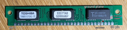
this also means that if you take a sharp hobby knife or the like and scrape away at the solder mask, you can expose or even cut the copper traces underneath, depending on whether you want to add or sever a connection somewhere.
Note that in this example (and in many other circuit boards) there's this very large and wide trace that covers most of the board where no other traces are present that I've labelled the ground plane - those are usually connected to either positive voltage or ground (in this case to ground via pins 9 and 22) and are used to provide easy access to either power or ground, plus their width means they can also pass much more current without overheating; in fact, if we were to compare this PCB to that of, say, a 100W+ something power supply...
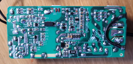
... you might notice the latter has some pretty beefy traces going around, especially towards the left and right ends of the PCB where the outputs and inputs respectively are located, due to the significant amounts of energy that might end up passing through those traces.
Meanwhile, most of the smaller traces and components are all primarily involved in regulating the behaviour of the larger and more powerful parts on the other side and therefore won't see all that much voltage or current. The big stuff is all topside and generally in contact with blocks of aluminium to act as heat sinks to prevent them from cooking themselves and releasing the magic smoke.
3 notes
·
View notes
Text
Sodium Persulfate’s Critical Role in PCB Etching Processes
Sodium persulfate is widely utilized in the electronics industry as an efficient etching agent for printed circuit boards (PCBs). Its strong oxidizing properties allow precise removal of copper, enabling intricate circuit designs. This ensures high-quality, reliable electronics production with consistent performance and scalability.

0 notes
Text
All About Materials for Printed Circuit Boards USA
Printed circuit boards (PCBs) in the US are mostly a flat laminated composite. PCB manufacturers use non-conductive substrate materials along with layers of copper circuitry on the external surfaces and buried in internal layers.
Printed circuit boards may be simple, with one or two layers of copper on the substrate, or complex, such as in high density applications, with more than fifty layers. Manufacturers use a flat composite surface, as this is ideal for mounting components that are ultimately attached to the copper layer by soldering. The copper traces interconnect the components electrically.
Basic Components and Materials of a Standard PCB
A standard PCB usually has six basic components:
Prepregs
Laminates
Copper Foil
Soldermask
Silk Screen
Surface Finish
Prepreg is made from a thin fabric of glass and coated with resin. Manufacturers cure the resin in special treaters. The glass fabric forms the basic mechanical support for holding the resin in place. The resin can be of various materials, like FR-4 epoxy, Teflon, Polyimide, and others. Initially, the resin is in a liquid form when coated onto the glass fabric. The combination moves through the treater, and the epoxy begins to dry as it travels through the oven section. Once it exits the treater, the epoxy is dry to touch.
When exposed to higher temperatures, usually above 300 °F, the resin in the prepreg begins to soften and melt. The resin soon reaches its thermosetting point, where it rehardens to become rigid again and very strong. Manufacturers use prepreg sheets to build the second component of a PCB — the laminate.
When laminated together with heat and pressure, sheets of prepreg and copper foil form the copper clad laminates for PCBs. Once the resin hardens, these PCB laminates with copper foil on both sides establish the basic structure of which PCB manufacturers make printed circuit boards.
To produce the circuitry on the laminate surface, the PCB fabricator must image and etch away the unwanted copper from the copper foil. These copper circuits create the tracks or conductors on the internal and external layers of the board. Once the fabricator images and etches each internal layer to constitute the circuits, they laminate them together using the prepreg.
Solder Mask is another epoxy coating on the board to cover the copper tracks on its outer layers. The coating protects the copper tracks on the external layers from oxidizing and corroding over time. As the internal circuitry remains buried within layers of prepreg, they do not need additional protection. Copper pads, where components will be soldered, are not covered by the soldermask.
Silk screen or nomenclature, forms the lettering on the PCB surface showing component numbers, their location, and their orientation. They can also show additional mounting information or handling precautions.
Besides the common green and white colors for the solder mask and silkscreen, manufacturers often use other colors also, in consultation with their customers.
Surface finish protects the copper pads left exposed by the soldermask. Fabricators use various types of surface finishes such as silver, tin/lead solder, lead-free solder, gold, nickel and others. Apart from protecting the exposed copper pads, surface finishes also provide a surface suitable for good solderability.
Selecting Materials for Printed Circuit Boards
Printed circuit board manufacturers offer a variety of materials for making the substrates and other components of PCBs. PCB designers select materials depending on the application requirements. Different material choices provide the PCB with varying qualities, facilitating the optimum performance for specific applications.
Designers make a choice of materials depending on:
Electrical performance — high voltage, high speed, high frequency
Mechanical performance — rigidity, flexibility, flame retardant
Thermal performance — ability to survive high temperatures, good thermal conductivity, low coefficient of thermal expansion
Regulatory/Governmental requirements — WEEE, RoHS, UL
For instance, a common popular consideration is complying with UL or Underwriters Laboratories requirements for flame retardation characteristics. Many electronic devices come with a UL rating to show that in the event of the device catching fire, the circuit board will retard the flames and will self-extinguish. This is a critical consideration for several types of consumer and other electronic equipment.
Resins and glass cloth fabrics that make up the laminates, must offer distinct insulating capabilities. Designers use different dielectric materials offering distinctive electrical and thermal characteristics for determining which laminate will best suit a PCB design for a specific application.
When making a material selection for their design, designers must consider various performance features. Most important among these are:
Dielectric Constant and Loss Factor — key electrical factors essential for high-speed performance and signal integrity.
High Glass Transition Temperature — capability to withstand high temperatures during assembly and field operation.
Flame Retardation — for UL qualification
Thermal Conductivity and Coefficient of Thermal Expansion — capability to perform in harsh service environments
Mechanical Strength and Dimensional Stability — mechanical attributes like shear and tensile strength when the PCB is in service, changes in dimension when manufacturing, undergoing thermal cycles during assembly, or when exposed to humidity.
Some Popular Materials for PCBs
FR-4 Prepreg and Laminates
FR-4 is the most popular PCB substrate material and is fire-retardant. The material has good thermal, electrical, and mechanical properties, along with a favorable strength-to-weight ratio as necessary for electronic applications. These are also one of the lowest cost PCB materials available.
Among printed circuit board manufacturers, FR-4 is a popular material for laminates and prepreg made from glass cloth and epoxy resins, for PCBs with low layer counts up to 14 layers. To improve its performance manufacturers often blend the epoxy resin with additives. This significantly improves its electrical, mechanical, and thermal properties, along with its ability to retard flames. Manufacturers use FR-4 laminates and prepregs as they are versatile, adaptable, and offer predictable yields.
Polyimide Prepreg and Laminates
For higher temperature performance compared to FR-4 materials, manufacturers use Polyimide laminates. Costing more than FR-4 materials, Polyimide materials offer better electrical performance, improved capacity to survive in higher temperature and harsh environments. With lower expansion characteristics, Polyimide materials are more stable during thermal cycling. Polyimide is more suitable for higher layer count PCBs.
Teflon Prepreg and Laminates
Bonding materials and laminates made of Teflon offer superior electrical properties, making them suitable for high-speed applications. Although more expensive than Polyimide materials are, Teflon offers designers better signal integrity in their designs. Printed circuit board manufacturers can enhance the characteristics of Teflon with special fillers and additives. Working with Teflon for PCBs requires specialized equipment and processing techniques.
Conclusion
Careful selection of materials for laminates and prepreg is necessary to ensure the Printed Circuit Board has the necessary electrical, dielectric, mechanical, and thermal properties for the end application.
Know More : https://www.pcbpower.us/blog/all-about-materials-for-printed-circuit-boards-usa
0 notes
Text
It is the foundation of electronic devices. The printed circuit board (PCB) connects electronic components and holds them in place by using conductive tracks etched onto a nonconductive surface, usually fiberglass. Imagine it as the nerve system of an electronic device. It tells components how to work together and where to send signals.
0 notes
Text
What Is Brass Sheet, Copper Sheet & the Best Metal for Reliable Performance?

Introduction: The Backbone of Quality Fabrication
From industrial workshops to architectural design studios, choosing the right sheet metal determines the quality, functionality, and longevity of your work. Whether you're crafting durable components, elegant fixtures, or high-precision parts, materials like the brass sheet, copper sheet, and globally trusted imported products stand out for their reliability.
In this blog, we’ll explain what each material is, where it’s best used, and how to select the best sheet metal for reliable performance in any project.
What Is a Brass Sheet?
A brass sheet is a flat-rolled alloy of copper and zinc, appreciated for its durability, corrosion resistance, and decorative appeal. It is used in both engineering and design contexts due to its strength and golden finish.
✔ Features of Brass Sheet:
Visual Appeal: Bright, gold-like appearance perfect for design
High Workability: Easily bent, cut, or engraved
Corrosion Resistance: Withstands moisture and salt air
Smooth Surface: Ideal for etching or engraving
✔ Best Uses:
Architectural hardware and design panels
Plumbing components and valves
Marine applications and instruments
Engraved nameplates and display boards
Choose from premium Brass Sheet options ideal for aesthetic and industrial-grade applications.
What Is a Copper Sheet?
A copper sheet is made from high-purity copper and is known for its excellent thermal conductivity, electrical properties, and antimicrobial capabilities.
✔ Why It’s Preferred:
Unmatched Conductivity: Ideal for electrical applications
Thermal Efficiency: Used in cooling and heating systems
Antimicrobial Surface: Makes it hygienic for healthcare and kitchens
Aging Gracefully: Forms a beautiful patina for weathered looks
✔ Best Applications:
Switchboards, wiring plates, and PCB boards
Copper roofs, domes, and flashings
Countertops, wall claddings, and kitchen surfaces
Renewable energy units and HVAC systems
Get certified and versatile Copper Sheet trusted across electrical and sanitary industries.
What Are Imported Products in Sheet Metal?
Imported products refer to high-grade metal sheets sourced from international manufacturers, known for their tight tolerance, premium finish, and global certifications like ISO, ASTM, and DIN.
✔ Advantages of Imported Sheets:
Global Compliance: Meets international quality standards
Superior Surface Quality: Available in mirror, matte, brushed, or coated
Specialty Materials: Includes bronze, nickel silver, and other alloys
Perfect for Automation: Ready for CNC, laser, and hydraulic presses
✔ Best Industrial Uses:
Aerospace components and instrumentation
Luxury architectural interiors and elevators
Medical equipment, enclosures, and consoles
High-end export products requiring consistent quality
Explore globally compliant Imported Products for quality that meets international demand.
What Is the Best Sheet for Reliable Results?
Here’s a quick guide comparing your three material options for performance: CategoryBrass SheetCopper SheetImported ProductsVisual AppealElegant Gold FinishRich Reddish ToneCustomizable (Mirror, Matte)Electrical UseModerateExcellentDepends on grade/alloyMechanical StrengthHighHighExtremely HighCertificationsIS/BISBIS/ASTMISO, ASTM, JIS, DINWeather ResistanceHighVery HighVaries (coated or alloy-based)
What Is the Best Thickness for Industrial Use?
Sheet thickness determines mechanical strength, weight capacity, and application suitability.
0.3 mm – 1 mm: Ideal for electronic panels, art, and interior cladding
1 mm – 3 mm: Best for furniture hardware, roof sheets, machine covers
3 mm – 6 mm+: Used in structural, load-bearing, or high-voltage systems
Imported sheets offer tight tolerance precision, making them excellent for robotic and automated use.
What Is the Best Surface Finish for Reliable Results?
Surface finish affects corrosion resistance, appearance, and post-fabrication effort. Finish TypeIdeal ForMirror PolishInteriors, nameplates, hotel lobbiesBrushed FinishKitchens, signage, elevatorsMatte FinishIndustrial or minimalist architectural stylesEmbossed/LaminatedDecorative and outdoor-use sheets
Imported products come pre-finished, which saves cost and ensures factory-grade consistency.
What Is the Best Way to Maintain Sheet Metal Performance?
✔ Storage Tips:
Keep flat with protective layers in low-humidity environments
Separate sheets with foam or plastic to prevent scratches
Avoid contact between dissimilar metals to prevent galvanic corrosion
✔ Maintenance Tips:
Brass Sheet: Clean with brass polish or a lemon-vinegar mixture
Copper Sheet: Let natural patina develop or use copper polish
Imported Sheets: Follow specific finish guidelines; avoid abrasive cleaning
Final Thoughts: Choose Materials That Stand the Test of Time
Choosing between a brass sheet, copper sheet, or imported products isn’t just about price—it’s about long-term performance, safety, and visual appeal. Brass offers beauty and corrosion resistance. Copper brings conductivity and hygiene. Imported materials offer global standards, precision, and versatility.
0 notes
Text

How is Aluminum PCB Made?
1. Material Selection: The primary material for Aluminum PCBs is an aluminum alloy, which acts as the base. This is paired with a thermally insulating layer and then a copper foil. The type of aluminum, insulating material, and copper thickness can vary based on the application.
2. Lamination: The layers are laminated together using heat and pressure. This ensures that the copper foil adheres well to the insulating layer, which in turn is bonded securely to the aluminum base.
3. Circuit Pattern Printing: Once laminated, the desired circuit pattern is printed onto the copper foil using a special ink. This ink acts as a protective barrier in the subsequent etching process.
4. Etching: The board is then subjected to an etching solution. This solution removes the exposed copper, leaving behind only the circuit pattern protected by the ink.
5. Drilling: Holes are drilled into the PCB for component leads or vias. This is done using precise CNC machines to ensure accuracy.
6. Surface Finish: To protect the exposed copper circuitry and improve solderability, a surface finish is applied. Common finishes include HASL (Hot Air Solder Leveling), ENIG (Electroless Nickel Immersion Gold), and OSP (Organic Solderability Preservatives).
7. Solder Mask Application: A solder mask is applied over the circuitry, leaving openings only where soldering will occur. This mask prevents accidental solder bridging during assembly.
8. Silkscreen Printing: For ease of assembly, reference designators and other important information are printed onto the PCB using ink.
9. Testing: Before shipping, the PCBs undergo electrical testing to ensure there are no shorts or open circuits.
10. Cutting and Profiling: The PCBs are then cut from the larger panel and profiled to the desired shape.
11. Final Inspection: A thorough visual inspection is done to ensure the PCB meets all quality standards.
The above process is a general overview, and specific processes will vary depending on the manufacturer and the intended application of the PCB.
0 notes
Text
Quality Control Standards for Printed Circuit Board Suppliers
In the fast-evolving world of electronics manufacturing, reliability and precision are not optional—they are essential. For businesses that rely on printed circuit boards (PCBs) to power their devices, quality assurance must be a top priority. At Pcb-Togo Electronic, Inc., we understand this responsibility. As a trusted Printed Circuit Board Supplier, we have built our reputation on a foundation of strict quality control standards designed to meet the most demanding performance and safety requirements.
Below, we explore the comprehensive approach we take at Pcb-Togo Electronic, Inc. to ensure every PCB we deliver is tested, traceable, and built to last.
Why Quality Control Is Critical for PCB Manufacturing
Unlike many components in the electronics supply chain, PCBs are the foundation of all electrical functionality in a device. Even a minor defect—such as a poor solder connection or microscopic short—can cause device failure, product recalls, or worse, safety hazards. For that reason, choosing a Printed Circuit Board Supplier with a proven quality control system is not just important—it’s mission-critical.
Poorly controlled PCB manufacturing can lead to:
Intermittent circuit failures
Early device breakdowns
Excessive rework costs
Damaged brand reputation
This is why at Pcb-Togo Electronic, Inc., we don’t just manufacture PCBs—we verify and validate every detail throughout the production process.
Our Quality Control Process: Built for Precision
At the core of our operations is a multi-phase quality control framework designed to ensure consistency, compliance, and performance. Our system covers every stage of PCB production, from material sourcing to final delivery.
1. Verified Materials and Supplier Audits
We begin quality control long before production starts. Every PCB at Pcb-Togo Electronic, Inc. starts with certified raw materials. We conduct strict inspections and maintain detailed supplier records to ensure that copper laminates, solder masks, and surface finishes meet global standards.
Regular supplier audits help us track quality at the source. Any vendor that fails to meet our benchmarks is removed from our approved list.
To explore how material quality affects PCB performance, Find Out More on our supplier verification page.
2. In-Process Inspections
Our in-house team conducts detailed inspections at every major production checkpoint:
Etching Accuracy – To prevent shorts or open circuits
Layer Alignment – Verified via X-ray scanning for multilayer boards
Hole Wall Quality – Assessed with microsectioning techniques
Solder Mask Integrity – Checked for uniform thickness and absence of bubbles
These real-time evaluations prevent defects from carrying forward, saving both time and cost. This proactive approach distinguishes us as a forward-thinking Printed Circuit Board Supplier.
3. Final Electrical Testing
No PCB leaves our facility without undergoing 100% electrical testing. Each board is verified for:
Continuity
Shorts
Component placement (if assembly is included)
Whether you're producing high-frequency boards or standard FR4 circuits, this final validation ensures that your boards will perform flawlessly in your application.
If you're curious about our advanced testing procedures, you can find out more by contacting our engineering team or viewing our testing guidelines online.
4. Strict Packaging & ESD Protection
Even after production, PCBs must be handled with care. Our packaging process includes:
Moisture barrier bags
ESD foam and shielding
Vacuum sealing for long-distance shipments
Each order is labeled for traceability, allowing clients to track batch origin, production data, and inspection results. This complete chain-of-custody approach ensures that your PCBs arrive in top condition—no matter where in the world you are.
For more on logistics and shipping support, go right here to our delivery resource center.
Continuous Quality Improvement (CQI)
Being a Printed Circuit Board Supplier means constantly adapting to evolving industry standards and customer requirements. At Pcb-Togo Electronic, Inc., we use data from inspections and customer feedback to refine our production lines. Our engineers regularly review:
First-pass yield rates
Customer return data
Root cause analyses
This commitment to Continuous Quality Improvement helps us remain flexible and responsive, while maintaining high yield rates and low defect percentages.
Why Choose Pcb-Togo Electronic, Inc.?
With over two decades of experience, we are a leading Printed Circuit Board Supplier known for our ability to deliver reliable, high-performance boards at competitive prices. What sets us apart is our end-to-end commitment to quality—from the raw copper to the final shipment box.
Clients from industries such as medical, automotive, aerospace, and consumer electronics trust us for:
Fast lead times
Transparent communication
Flexible order quantities
Proven reliability
When you partner with Pcb-Togo Electronic, Inc., you’re choosing a supplier that backs every board with traceability, testing, and total accountability.
Final Thoughts
Selecting a reliable Printed Circuit Board Supplier is essential to the long-term success of any electronics product. At Pcb-Togo Electronic, Inc., quality isn’t a department—it’s the DNA of our entire operation. From stringent inspections and automated testing to supplier audits and proactive improvement, we take every step necessary to ensure our PCBs are ready for real-world performance.
If you’re ready to raise the bar for your electronics production, Find Out More by speaking with our technical experts or requesting a custom quote today.
Original Link: https://pcbtogo.blogspot.com/2025/06/quality-control-standards-for-printed.html
0 notes
Text
0 notes
Text

Sodium Persulfate’s Critical Role in PCB Etching Processes
Sodium persulfate is widely utilized in the electronics industry as an efficient etching agent for printed circuit boards (PCBs). Its strong oxidizing properties allow precise removal of copper, enabling intricate circuit designs. This ensures high-quality, reliable electronics production with consistent performance and scalability.
Source - https://calibrechem.com/blog/sodium-persulfate-applications-in-printed-circuit-board-etching-and-electronics-manufacturing/
0 notes
Text
Improve Air Quality with a High-Efficiency Fume Absorber in India
In industrial and electronic workspaces, airborne contaminants are a silent threat. Whether you’re soldering PCBs or working in chemical labs, exposure to harmful fumes can cause serious health issues and affect overall productivity. This is why investing in a reliable fume absorber in India is not just a choice—it's a necessity. At Ascomp Inc., we offer cutting-edge fume absorbers that ensure cleaner air and a safer work environment.
Our fume absorbers are designed to eliminate smoke, dust, gases, and toxic particles from the air, making them essential for electronics assembly units, medical labs, manufacturing floors, and educational institutions. With growing environmental and safety regulations, having a high-quality fume absorber has become a standard for responsible businesses.
What Is a Fume Absorber?
A fume absorber in India is a compact air filtration device that captures hazardous airborne substances at the source. It typically uses a combination of filters—such as HEPA and activated carbon—to remove particulates and neutralize toxic gases before recirculating clean air into the environment.
The key advantage of a fume absorber is that it prevents workers from inhaling harmful fumes generated during processes like soldering, laser engraving, chemical etching, or solvent use. This significantly reduces the risk of respiratory issues, eye irritation, and long-term health hazards.
Features of Ascomp Inc. Fume Absorbers
Our fume absorbers come with:
High-Efficiency Filtration: Multi-stage filtration system including pre-filter, HEPA filter, and activated carbon layer.
Low Noise Operation: Quiet motors ensure minimal disruption in the workplace.
Flexible Arm Design: Adjustable suction arms allow you to position the unit directly over the fume source.
Portable & Compact: Space-saving design makes it ideal for crowded workstations.
Energy Efficient: Low power consumption without compromising performance.
Easy Maintenance: Quick filter replacement and minimal downtime.
Applications of Fume Absorber in India
As the demand for clean air solutions increases, our fume absorber in India is becoming a staple in:
Electronics Manufacturing: Removing solder fumes and flux residue.
Pharmaceutical and Medical Labs: Filtering chemical vapors and biological particles.
Laser and Engraving Workshops: Absorbing smoke from burning materials.
Jewelry Workshops: Removing fumes from polishing and soldering.
Schools and Training Institutes: Safe demonstration of chemistry and electronics.
Why Choose Ascomp Inc.?
Industry Experience: Trusted by industrial clients and academic institutions alike.
Custom Solutions: Models available for single or multi-user workstations.
Local Support: Quick service and spare parts availability across India.
Quality Assurance: Products tested for filtration efficiency and durability.
Affordable Pricing: Competitively priced to deliver best value.
#FumeAbsorberIndia#CleanAirSolutions#AscompInc#SolderingSafety#IndustrialAirFiltration#ESDWorkstation#WorkplaceSafety#ElectronicsManufacturing#AirPurifierIndia#LabSafety
0 notes
Text
Dry Film Etching Machine Market to Reach $796.2 Million by 2035
The Dry Film Etching Machine market is projected to experience significant growth, with industry revenue expected to rise from $475.4 million in 2024 to $796.2 million by 2035. This growth is driven by increased demand in several key applications, including semiconductor manufacturing, printed circuit board (PCB) fabrication, photovoltaic cell production, and material research.
Detailed Analysis - https://datastringconsulting.com/industry-analysis/dry-film-etching-machine-market-research-report
Key Applications Driving Market Growth
Dry Film Etching Machines are essential in the semiconductor sector, particularly for the creation of circuits through precise manufacturing processes. Methods such as plasma etching and reactive ion etching provide the high accuracy and precision required for complex components. Leading semiconductor companies like Intel Corp and Samsung Electronics rely on these machines to maintain control over etching depth, which enhances their manufacturing capabilities and strengthens their position in the market.
These machines are also critical in the production of Microelectromechanical Systems (MEMS), which include small-scale devices like sensors and actuators. Companies such as Texas Instruments and Analog Devices use Dry Film Etching Machines to produce MEMS devices, helping them enhance their market position through technological innovation.
Transition Toward Nanoscale Etching
The market is shifting from traditional etching methods to nanoscale etching processes, driven by the growing need for nanodevices in electronics and healthcare. This trend signifies significant ongoing development in the industry, enabling the creation of smaller, more intricate components. Advances in dry film etching methods are particularly evident in the development of integrated circuits, which are now essential to modern electronics.
Industry Leadership and Strategies
The Dry Film Etching Machine market is highly competitive, with major players like:
Applied Materials Inc.
Tokyo Electron Limited
Hitachi High-Technologies Corporation
Lam Research Corporation
ASM International
KLA-Tencor Corporation
Canon Anelva Corporation
Advanced Micro-Fabrication Equipment
Plasma-Therm
Technics Plasma GmbH
Oxford Instruments
These companies are actively driving innovation through strategic initiatives, such as expanding production capacity, developing high-precision etching techniques, and improving efficiency to reduce manufacturing costs.
Market Drivers and Growth Opportunities
The Dry Film Etching Machine market is expected to expand significantly between 2025 and 2030, driven by factors like:
Increased semiconductor production
Growth in the LED market
Advancements in nanotechnology
As these technologies advance, new opportunities are emerging in developing economies, further accelerating market growth.
Regional Analysis
North America remains a key player in the Dry Film Etching Machine market, primarily due to its advanced technology sector and significant investments in semiconductor industries. The competition among manufacturers in this region is fierce, which drives innovation and the incorporation of new technologies into products to enhance market presence. Factors contributing to growth in North America include extensive research and development, increasing use of IoT applications, and a focus on enhancing semiconductor manufacturing efficiency. The United States, in particular, offers growth potential due to its prominent semiconductor firms and rising demand for energy-saving devices.
Comprehensive Market Insights
The global Dry Film Etching Machine market is analyzed in detail, covering various technology types such as:
Plasma Etching
Laser Ablation
Ion Milling
Additionally, the market is segmented by application areas like:
Semiconductors
Microelectronics
Photovoltaic Cells
Integrated Circuits
Others
It also includes insights into customer scales, ranging from small-scale enterprises to large-scale enterprises, across more than 20 countries.
About DataString Consulting
DataString Consulting helps businesses formulate strategies and create roadmaps, including Total Addressable Market (TAM) expansion, revenue diversification, and venturing into new markets. The firm provides in-depth insights into emerging trends, competitor landscapes, and customer demographics, enabling businesses to seize new opportunities and reduce time-to-market.
With over 30 years of combined experience, DataString’s leadership team offers tailored market research and business intelligence solutions for both B2B and B2C markets. The firm’s experts continuously track high-growth segments across 15+ industries and 60 sub-industries, providing clients with the insights needed to make informed decisions and foster long-term success.
0 notes