#systemverilog
Explore tagged Tumblr posts
Visit Tumblr Blog
Explore Tumblr blogs with no restrictions, modern design and the best experience.
Last Seen Tumblr Blogs


Fun Fact
Tumblr Inc. is funded by 13 investors.
Text
celebrating fall with fletcher's checksum
This post originally appeared on my website.
why are checksums useful for fpga development?
Checksum functions are useful for error detection and data integrity. With respect to FPGA architecture development, a checksum can ensure the system is able to retain its state. For example, an FPGA programmed to behave like an AND gate should not start to act like an OR gate due fluctuations in voltage or temperature. Such problems may be caught by computing the checksum of the bitstream before configuring the FPGA, operating the device in the lab, and then extracting the bitstream and re-computing the checksum to ensure it has not changed.
The last two FPGAs that I worked on-with Indiana University's SAIL-IN Lab and the QuickLogic Corporation-used a scan chain configuration interface which lent itself well to bitstream verification via checksum. The scan chain acts like a serial shift register, stringing together all the configuration chain flip-flops in the FPGA fabric. As the bitstream flows through the head of the scan chain, one bit at a time, its checksum may be computed; and later re-computed as it flows out of the tail. For context, imagine a small, thirty-two flop scan chain and the corresponding bitstream, 0xdeadbeef. On the way in, the Fletcher's (32-bit) checksum will be 0xf13b. If the post-configuration checksum does not match, the engineers would know that there is an issue with the FPGA architecture.
Fletcher's checksum also produces check bytes (or a "tag"), which can be appended to the end of the original data, such that the new checksum of the data and the check bytes is zero. For the example bitstream 0xdeadbeef, the resulting check bytes are 0xd2f1. And the checksum of 0xdeadbeefd2f1 is 0x0.
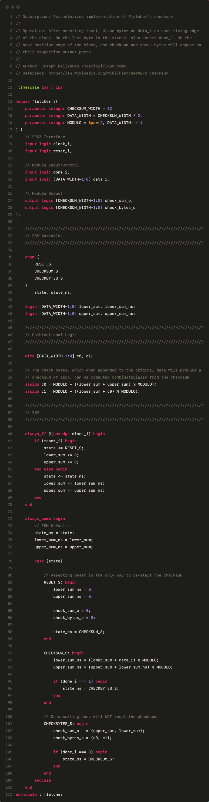
fletcher's checksum in systemverilog
Based mostly on the Wikipedia entry for Fletcher's checksum, I produced a parameterized, three-state module which computes the checksum and check bytes of a data stream. The SystemVerilog closesly follows the below psuedo-code. For the Fletcher-32 checksum, data arrives as 16-bit half-words.
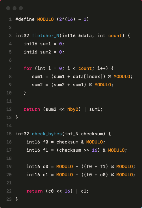
Eventually, I'd like to wrap it in a SPI interface and submit it to TinyTapeout, but for now here's the bare RTL. The most up-to-date code is also available on GitHub:
#engineering#computer engineering#fpga#verilog#systemverilog#hardware design#engineering student#studyblr
1 note
·
View note
Text
Verilog Interview Questions for Freshers & Experienced | Maven Silicon
Get Verilog & DFT Interview Questions and Answers for Freshers and Experienced candidates which help you to get ready for a job interview. For most asked Verilog interview questions, read now!
0 notes
Text
Paving the Path to VLSI Success: A Deep Dive into Learning Opportunities
The Rising Demand for VLSI Professionals
In today’s technology-driven world, the demand for skilled professionals in the field of Very-Large-Scale Integration (VLSI) continues to surge. VLSI technology forms the foundation of most modern electronic devices, from smartphones to satellites. As integrated circuits become more complex, the need for engineers who can design, test, and improve these systems grows. Engineering students and electronics graduates looking to future-proof their careers are increasingly drawn to VLSI as a specialization. Companies in India and around the world are on the lookout for talent equipped with practical VLSI skills, making this an attractive career path. Given this scenario, educational institutions and private training centers have stepped up to provide in-depth programs designed to meet industry needs. Aspiring engineers now have a variety of options to choose from when selecting the right program to build their foundation in VLSI technology.
Importance of Industry-Relevant Training in VLSI
While a formal degree in electronics or electrical engineering provides the basics, industry-relevant training in VLSI is critical for practical success. This is because VLSI is highly application-based, demanding a strong understanding of design tools, programming languages, and testing methodologies. Hands-on experience with CAD tools, simulation software, and real-time projects can make all the difference. As a result, the choice of a training institute becomes an important factor. Students looking to enter this domain often search for the top vlsi institutes in hyderabad, as Hyderabad is a major technology hub with several reputed centers offering quality training. These institutes focus on practical exposure, experienced faculty, and placement support, all of which are key to student success. With proper guidance and the right learning environment, students can gain the skills required to thrive in this competitive field.
Choosing the Right VLSI Course
Selecting the right VLSI course is essential for aligning one's career goals with market expectations. The ideal course not only covers theoretical knowledge but also emphasizes real-world application. Curriculum components typically include digital design, CMOS technology, Verilog/VHDL, ASIC design, and FPGA implementation. Additionally, courses offering modules on SystemVerilog, UVM, and embedded systems are becoming increasingly popular. When evaluating course offerings, many prospective students explore vlsi courses in hyderabad to find a comprehensive program that covers both front-end and back-end design processes. It is important for learners to also consider the duration, mode of delivery (online/offline), and availability of project work. A structured course with industry-certified trainers and access to advanced lab setups can provide a valuable edge in this field. This clarity helps learners not only gain knowledge but also build a strong portfolio that can appeal to future employers.
Placement Support and Career Opportunities
One of the biggest advantages of enrolling in a reputed VLSI training program is the access to placement support. Leading institutes often have tie-ups with semiconductor companies, startups, and multinational corporations looking for trained professionals. Career opportunities in VLSI are vast, ranging from physical design engineers to verification specialists and DFT engineers. With the growth of IoT, AI, and 5G technologies, VLSI engineers are finding exciting roles in hardware development teams across domains. Institutes that focus on industry connections, mock interviews, resume building, and internships significantly boost a student’s employability. Moreover, alumni networks and mentorship programs help learners stay updated on trends and job openings. A combination of technical skills and soft skills training can greatly improve the likelihood of landing a dream role. As the semiconductor industry continues to grow, so too does the demand for qualified, hands-on VLSI professionals.
Conclusion: Begin Your VLSI Journey with Confidence
Choosing the right institute and course is the first step toward a successful VLSI career. From understanding the fundamentals to mastering design and verification tools, a structured training program can be a game changer. Whether you're a fresh graduate or a working professional looking to switch domains, VLSI offers a dynamic and rewarding path. Hyderabad, as a tech hub, continues to provide ample opportunities for learning and growth in this field. Institutes that combine practical training, expert mentorship, and placement assistance can help bridge the gap between education and employment. If you're looking to start or elevate your career in this domain, takshila-vlsi.com is a reliable place to begin your journey.
0 notes
Text
Build a Career in VLSI with RTL Verification and ASIC Design Courses at Takshila Institute
The world of VLSI design is built on strong foundations in RTL (Register Transfer Level) verification and ASIC (Application-Specific Integrated Circuit) design. These two areas are critical to ensuring that semiconductor chips are not only well-designed but also function as intended before fabrication. Takshila Institute of VLSI Technologies in India has emerged as a trusted name, offering advanced training through its RTL verification training institutes and comprehensive ASIC design course online, empowering learners with practical skills for real-world chip development.
Industry-Relevant RTL Verification Training
Takshila Institute of VLSI Technologies offers specialized programs through its RTL verification training institutes aimed at fresh graduates and working professionals. The course focuses on key aspects such as SystemVerilog, UVM (Universal Verification Methodology), functional coverage, assertions, testbench architecture, and simulation-based verification techniques. Students gain hands-on experience using top EDA tools widely adopted in the semiconductor industry. By solving live projects and learning from industry experts, students are trained to identify, debug, and fix design issues at the RTL level effectively.
Learn ASIC Design Anytime with Online Courses
Takshila also provides a well-structured ASIC design course online that caters to learners who prefer flexible and remote learning options. The online course includes modules on RTL design, synthesis, floorplanning, timing analysis, design optimization, and low-power techniques. The course content is delivered through live virtual classes, recorded sessions, interactive labs, and mentor-led projects, ensuring that distance learners receive the same depth and quality as in-classroom students. The course is designed to simulate an actual design environment, preparing students for real-time ASIC development tasks.
Why Choose Takshila Institute of VLSI Technologies?
The success of Takshila Institute of VLSI Technologies lies in its industry-focused curriculum, experienced trainers, modern lab infrastructure, and strong placement support. Whether learning on campus or online, students benefit from continuous mentorship and guidance that goes beyond just completing the course. The institute is known for transforming beginners into skilled VLSI engineers, ready to take on complex verification and ASIC design roles.
Conclusion
If you're looking to start or enhance your career in semiconductor design, Takshila Institute of VLSI Technologies in India provides the perfect platform. With its expert-led RTL verification training institutes and flexible ASIC design course online, Takshila empowers students with the technical expertise and confidence needed to succeed in the competitive VLSI industry.
0 notes
Text
Mastering VLSI Design: The Path to a Promising Career in Semiconductor Industry
The Rising Demand for VLSI Professionals
The semiconductor industry is experiencing a dramatic shift, powered by the growing demand for smaller, faster, and more efficient chips in everything from smartphones to electric vehicles. Very-Large-Scale Integration (VLSI) design plays a critical role in this transformation, enabling the integration of millions of transistors onto a single chip. As technology continues to evolve, the need for skilled VLSI engineers is expanding at an unprecedented rate. This demand has opened up a world of opportunities for those interested in chip design and semiconductor engineering. Companies worldwide are investing in VLSI talent to maintain a competitive edge, making this an ideal time for students and professionals to build a career in the field. Whether it’s designing system-on-chip (SoC) solutions or optimizing embedded systems, VLSI experts are becoming increasingly vital to the tech ecosystem.
Understanding the Fundamentals of VLSI Design
VLSI design involves the process of creating integrated circuits by combining thousands or even millions of transistors into a single chip. This complex engineering task requires a deep understanding of electronic circuit design, semiconductor physics, and design tools like Verilog, SystemVerilog, and VHDL. The curriculum in most vlsi training institutes includes modules on front-end and back-end design, logic synthesis, timing analysis, and verification methods. The end goal is to produce high-performance chips that are also power-efficient and cost-effective. VLSI engineers must possess strong analytical skills, a deep interest in electronics, and a passion for solving real-world problems. As technology nodes continue to shrink from 7nm to 3nm and beyond, the challenges in VLSI design grow more complex—demanding not just theoretical knowledge but also hands-on experience in state-of-the-art tools and practices.
Exploring Career Opportunities in VLSI
A career in VLSI is not only intellectually rewarding but also financially lucrative. From design engineers to physical design experts and verification engineers, the job roles in this domain are diverse and highly specialized. Each position plays a crucial part in bringing a semiconductor product from concept to fabrication. What makes VLSI especially appealing is the steady demand from both startups and tech giants involved in AI, IoT, and 5G innovation. Particularly in India, the ecosystem around semiconductor design is growing, creating an urgent need for competent professionals. The rise of online vlsi training institutes in bangalore has made it easier for aspiring engineers to access high-quality education and training without geographical constraints. With remote learning tools, recorded sessions, and access to simulators, these platforms are revolutionizing how VLSI education is delivered, allowing learners to gain industry-relevant skills from the comfort of their homes.
Key Skills and Tools Every VLSI Engineer Should Learn
To thrive in the VLSI domain, aspiring engineers must master a combination of technical skills and practical tools. On the technical side, knowledge of digital electronics, CMOS design principles, and signal integrity is foundational. On the software front, proficiency in EDA (Electronic Design Automation) tools like Cadence, Synopsys, and Mentor Graphics is a must. Additionally, scripting languages such as Perl, Python, and Tcl are used to automate repetitive design and verification tasks. Industry expectations are high, and candidates are often evaluated not just for their academic background but for their problem-solving ability, project experience, and understanding of real-time design constraints. VLSI is a continuously evolving field, and engineers must commit to lifelong learning to stay ahead. Regularly updating one’s knowledge through webinars, certifications, and self-guided projects is crucial to success in this fast-paced industry.
Choosing the Right Institute for VLSI Training
Given the complexity and depth of the VLSI field, selecting the right training institute becomes a vital step in one’s professional journey. The ideal institute offers a blend of theoretical instruction and practical exposure, mentored by industry veterans. It should provide access to real-world design tools, capstone projects, and placement support. Moreover, flexibility in learning schedules and a structured curriculum aligned with industry requirements can make a significant difference. One such platform that offers all these features is takshila-vlsi.com, a trusted name in the VLSI education space. With a commitment to quality and innovation, Takshila VLSI equips learners with the skills needed to succeed in the semiconductor industry, bridging the gap between academic knowledge and practical application.
0 notes
Text
Will AI Eliminate Verification?

A recent blog post looked at the impact artificial intelligence (AI) is having on chip development, focusing on register-transfer-level (RTL) design in general, and the hardware-software interface (HSI) in particular. It seems natural to extend this topic to ask how AI is affecting functional verification of chip designs. Again, there’s plenty of hype on this topic, but it’s important to separate “perhaps someday” visions from the current reality of what AI can accomplish.
AI and IP Verification
The recent post noted that the generation of RTL designs is a domain where AI has shown some success. It used the example of asking ChatGPT to “generate SystemVerilog code for an 8-bit priority encoder” and showed its output. In theory, such generated designs should be “correct by construction” since AI tools are trained on huge datasets that include many successful real-world RTL IP designs. Does this mean that they don’t need to be verified?
The answer, of course, is “no!” since training datasets may include designs with bugs in them, resulting in a large language model (LLM) with errors. In addition, the well documented tendency of AI tools to hallucinate means that the output may sometimes not make sense. It is important to verify any RTL code generated by AI, just as code written by humans. This verification may happen in a standalone IP block testbench, in higher levels of the chip hierarchy, or both.
This leads to the question of whether AI can generate the verification testbench and tests. Typing “generate SystemVerilog UVM testbench and tests for an 8-bit priority encoder” into ChatGPT yields a basic solution that includes a top-level testbench, UVM agent, driver, monitor, and scoreboard, plus a sequence (shown below) with a few common tests. It’s a good start, although an experienced verification engineer would want to add coverage and some additional tests.class priority_encoder_sequence extends uvm_sequence #(priority_encoder_transaction); // Constructor function new(string name = "priority_encoder_sequence"); super.new(name); endfunction // Generate test cases virtual task body(); priority_encoder_transaction tx; // Test case 1: All zeros tx = priority_encoder_transaction::type_id::create("tx"); tx.in_data = 8'b00000000; start_item(tx); finish_item(tx); // Test case 2: Only one bit set tx.in_data = 8'b00000100; start_item(tx); finish_item(tx); // Test case 3: Multiple bits set tx.in_data = 8'b11000000; start_item(tx); finish_item(tx); // Test case 4: All ones tx.in_data = 8'b11111111; start_item(tx); finish_item(tx); endtask endclass
AI and SoC Verification
It seems likely that any AI tool capable of generating an RTL IP block is also capable of generating a standalone testbench and some basic tests. These could also be used to verify a hand-written IP block, or one generated by a different AI tool or LLM. Of course, it is important to verify at least some of the functionality of an IP block once it is instantiated into the chip design. Since AI is not today able to generate the RTL design for a complete chip, it is unreasonable to expect that it could verify one.
Fortunately, there are some aspects of a complex chip that can be verified by current AI tools. The previous post focused on the HSI, which is an essential part of any system on chip (SoC), and on the generation of the memory-mapped, addressable control and status registers (CSRs) that form the hardware side of the HSI. Generating a testbench and tests to verify a CSR block certainly seems within the scope of AI as well.
Thorough hardware-software verification of the HSI involves both the CSR hardware and the low-level software (such as microcode and device drivers) that programs the registers. HSI verification requires tests that exercise the registers and check the results. Many of these tests could potentially be generated by AI tools, although custom sequences that access the registers may be needed. Thus, there must be a way to specify these sequences as well as the set of registers.
Agnisys AI Verification Solutions
The Agnisys IDesignSpec™ Suite is a specification automation solution that generates register RTL code, SystemVerilog Open Verification Methodology (OVM) testbenches and tests, C/C++ tests, and combined hardware-software verification environments. As discussed in the earlier post, the Agnisys SmartDatasheet site uses leading-edge LLM and natural language processing (NLP) technology to interpret natural language datasheets with CSR definitions to generate the RTL code.
IDesignSpec uses the same register definitions, whether from datasheets or from standard formats such as SystemRDL and IP-XACT, to generate verification testbenches and tests. The C/C++ tests can be run on UVM testbenches, co-verification environments, emulators, and even actual chips. The tests are fine-tuned for any special registers specified, including indirect, indexed, read-only/write-only, alias, lock, shadow, interrupt, counter, paged, virtual, external, and read/write pairs.
When custom CSR programming sequences are required, Agnisys provides an AI solution as well. Users can write these sequences in natural language, which is converted via NLP into UVM and C/C++ sequences. Assertions, an important part of RTL verification, can also be specified as statements of design intent in natural language. The Agnisys iSpec.ai site converts these statements into SystemVerilog Assertions (SVA), which could be for the CSRs or any other parts of the design.
Summary
AI is a long way from generating a full-chip testbench and a complete set of tests, but it adds value to the verification flow today for assertions, CSR programming sequences, and HSI testbenches. This frees up a lot of time for the verification engineers, enabling them to focus on more complex chip-level tests. Agnisys is a proven industry leader in using AI for SoC and IP development, with additional capabilities in development.
0 notes
Text
Master ASIC Design and Verification Training Today

In today’s fast-paced semiconductor industry, mastering ASIC (Application-Specific Integrated Circuit) design and verification is essential for engineers and professionals looking to advance their careers. With cutting-edge technology and increasing demand for customized chip designs, the need for skilled ASIC designers is greater than ever. If you are eager to enhance your expertise, ASIC Design and Verification Training is the perfect opportunity to gain in-depth knowledge and practical skills.
Why Choose ASIC Design and Verification Training?
ASIC design is a complex yet rewarding field that requires a deep understanding of digital circuits, system architecture, and verification methodologies. This training equips you with:
Fundamental and Advanced ASIC Design Concepts – Learn the principles of ASIC development, from design to implementation.
Verification Techniques – Master simulation-based verification, formal verification, and functional testing.
Industry-Standard Tools – Get hands-on experience with tools like Verilog, VHDL, SystemVerilog, and UVM.
Practical Projects and Case Studies – Work on real-world projects to strengthen your problem-solving abilities.
Expert Guidance – Learn from industry professionals with years of experience in ASIC design and verification.
Who Should Enroll?
This training is ideal for:
Engineering students and graduates looking to specialize in VLSI and ASIC design.
Working professionals aiming to upskill in semiconductor design.
Anyone passionate about learning digital design and verification methodologies.
Career Benefits of ASIC Design and Verification Online Training
With expertise in ASIC design and verification, you can unlock various career opportunities in semiconductor and electronics industries. Job roles include:
ASIC Design Engineer
Verification Engineer
FPGA Engineer
VLSI Design Engineer
Embedded Systems Engineer
Enroll Today and Advance Your Career!
Don’t miss the chance to boost your career in the high-demand field of ASIC design. Join ASIC Design and Verification Training today and gain the skills needed to thrive in the semiconductor industry. Start your journey towards success with expert-led training and hands-on experience.
At Multisoft Virtual Academy, we provide comprehensive training programs to help tech enthusiasts achieve professional excellence. Sign up now and take the next step in your career!
0 notes
Text
CS223 Laboratory Assignment 3 Modeling Decoders and MUXs in System Verilog
Location: EA Z04 (in the EA building, straight ahead past the elevators) Each student should attend the time block depending on their student id. A student with student id 22050977(Odd) from section 4 should attend lab at 10:00 am on Friday for example. Preliminary Report (30 points) Today’s lab needs considerable advance preparation. These advance designs and SystemVerilog models should be…
0 notes
Text
FPGA - Step 1: Understand the Project Requirements Solved
Before starting, review the overall goals of the project: Objective: Implement a simple 10-bit processor on an FPGA using SystemVerilog. Key Features: 10-bit data bus architecture. 1024×10 RAM module for both program and data storage. Register file with various addressing modes. Multi-stage ALU for arithmetic and logical operations. Output system using three 7-segment displays and LED…
0 notes
Text
Systemverilog??? Not again 😭 I've had enough
1 note
·
View note
Text
Linux Kernel Developer Internship in Surat at Vicharak Computers LLP
evolve, they will become more accelerated. Utilizing FPGA reconfigurable hardware and Verilog/SystemVerilog logic design… Apply Now
0 notes
Text
Verilog Interview Questions for Freshers & Experienced | Maven Silicon
Get Verilog & DFT Interview Questions and Answers for Freshers and Experienced candidates which help you to get ready for a job interview. For most asked Verilog interview questions, read now!
0 notes
Text
Discover the Right VLSI Training Destination to Shape a Bright Career
The Growing Demand for VLSI Professionals The world is moving rapidly towards automation, smart electronics, and cutting-edge semiconductor technologies. As a result, VLSI (Very Large Scale Integration) has become a crucial domain in the electronics industry. It plays a significant role in designing compact, high-performance integrated circuits that power modern electronic devices. This increasing reliance on microchips has sparked a strong demand for skilled VLSI professionals across India and beyond. For those aiming to build a career in semiconductor design, selecting the right training institute becomes the first and most important step.
Why Hyderabad is a Preferred City for VLSI Training Hyderabad has emerged as a major hub for semiconductor companies and research institutions, making it an ideal location for VLSI training. The presence of leading IT parks, development centers, and electronics manufacturing companies has led to the establishment of several reputed training institutes. Among the top vlsi training institutes in hyderabad, students often seek those that offer practical learning, expert faculty, and strong placement support. These institutes are known for their industry-oriented curriculum, state-of-the-art labs, and real-time project training. Hyderabad continues to attract VLSI aspirants due to its affordable cost of living, quality education, and vast opportunities in the electronics sector.
Essential Features of a Good VLSI Training Program A quality VLSI training program focuses not only on theoretical knowledge but also on practical skills development. It typically covers ASIC design, FPGA design, Verilog, VHDL, SystemVerilog, and related tools such as Cadence and Synopsys. The use of real-time projects allows students to gain confidence and familiarity with industry practices. Faculty with real-world experience in chip design and verification can make a huge difference in understanding the practical challenges of VLSI projects. A good institute should also provide access to placement assistance, resume preparation, and interview coaching to enhance employability.
Key Factors to Consider While Choosing a VLSI Institute Selecting the right institute can have a long-lasting impact on one’s career. Factors such as the curriculum, infrastructure, faculty experience, placement records, and alumni feedback should be considered carefully. Also, institutes that maintain strong industry collaborations often provide better internship and job opportunities. Personalized mentorship, exposure to real-time tools, and soft skills training further improve the chances of landing a job in reputed companies. Ensuring these elements are part of the training structure can help learners stay ahead in the competitive VLSI job market.
Bangalore’s Role in Advancing VLSI Careers Bangalore, known as India’s Silicon Valley, also stands tall in offering top-tier VLSI education. It is home to several reputed vlsi training institutes in bangalore, many of which have strong industry connections and advanced lab facilities. The proximity to global semiconductor giants and tech startups makes Bangalore an ideal location for gaining hands-on experience. Institutes in the city are known for organizing workshops, internships, and campus placements that prepare students for real-world job roles in VLSI design and verification. The exposure to an innovation-driven environment gives learners an added advantage in shaping a successful career.
Conclusion VLSI is a fast-evolving field that requires focused training and continuous upskilling. Choosing a city like Hyderabad or Bangalore, both equipped with academic excellence and industry presence, can significantly boost one’s career prospects. Whether enrolling in one of the top vlsi training institutes in hyderabad or exploring options among the vlsi training institutes in bangalore, learners should evaluate all aspects of a training program before committing. In the middle of this growing demand, Takshila Institute of VLSI Technologies has gained recognition for providing high-quality education and consistent placement support. Ultimately, the right training from a credible institute can open doors to a rewarding future in the semiconductor industry.
0 notes
Text
Leading SystemVerilog and Verilog Training Institute in India
In today’s rapidly advancing semiconductor industry, knowledge of hardware description languages like Verilog and SystemVerilog is essential for anyone aiming to build a successful career in VLSI design and verification. Among the institutes offering quality training in this domain, Takshila Institute of VLSI Technologies has emerged as a top destination for professionals and students alike. Renowned for its comprehensive programs, it is widely recognized as one of the best System Verilog training institutes in Hyderabad and a trusted name for those seeking Verilog training institutes in Bangalore.
Takshila Institute of VLSI Technologies offers specialized training programs designed to provide in-depth understanding of Verilog and SystemVerilog, focusing on both RTL design and functional verification. The course begins with the fundamentals of digital design and gradually progresses to advanced topics such as constrained random verification, assertions, coverage analysis, and testbench architecture. This structured approach ensures that learners develop strong coding skills along with practical application in industry-level projects.
As one of the most sought-after SystemVerilog training institutes in Hyderabad, Takshila stands out for its hands-on teaching methodology. Students are trained using real-time projects and industry-standard EDA tools, enabling them to gain practical exposure that goes far beyond textbook learning. The institute's expert faculty, who bring years of industry experience, provide personalized guidance and mentorship throughout the course.
In addition, Takshila Institute is well known among learners seeking Verilog training institutes in Bangalore, thanks to its reputation for delivering high-quality online and hybrid learning options. Students from across the country enroll in its training programs due to the institute’s proven track record of successful placements, strong curriculum, and focus on career readiness.
What makes Takshila unique is its emphasis on both design and verification aspects. Whether you’re a beginner looking to learn Verilog from scratch or an experienced engineer aiming to master SystemVerilog for verification roles, the institute provides a pathway that aligns with individual career goals. Mock interviews, technical assessments, and resume preparation sessions are also part of the course to support students in their job search.
For those aspiring to become skilled VLSI engineers, Takshila Institute of VLSI Technologies offers the perfect blend of theoretical knowledge and practical experience. Recognized among the best SystemVerilog training institutes in Hyderabad and preferred by many searching for Verilog training institutes in Bangalore, Takshila is committed to empowering the next generation of semiconductor professionals with top-tier education and industry-aligned skills.
0 notes
Text
One of the Top VLSI Institutes and a Leading Online VLSI Training Provider
For aspiring semiconductor professionals seeking the top VLSI institutes in Bangalore, Takshila Institute of VLSI Technologies is a name that consistently earns recognition for its focused and high-quality training. Although headquartered in Hyderabad, Takshila has established itself as a national leader in VLSI education, including robust online VLSI institute offerings that cater to learners across India. Its advanced curriculum, industry-experienced faculty, and strong placement support make it a preferred destination for students and professionals aiming to build a career in VLSI design and verification.
VLSI (Very-Large-Scale Integration) technology is at the heart of modern electronics, powering everything from smartphones to data centers. With this growing demand, Takshila Institute of VLSI Technologies offers specialized courses in key domains such as RTL design, verification using SystemVerilog and UVM, physical design, DFT (Design for Testability), and analog/mixed-signal IC design. Each program is carefully designed to align with industry requirements, ensuring that learners are well-equipped with practical skills and technical knowledge.
For those searching for the top VLSI institutes in Bangalore, Takshila’s reputation extends well beyond geographical boundaries due to its strong online presence. Its online VLSI institutes provide comprehensive, flexible, and accessible learning experiences that match the quality of its classroom training. With live sessions, recorded lectures, hands-on projects, and one-on-one mentorship, the online programs cater to students, fresh graduates, and working professionals who need the convenience of remote learning without compromising on content depth or job readiness.
Takshila’s faculty are experienced VLSI engineers with a strong background in both teaching and industry projects. Their mentorship is a cornerstone of the learning process, helping students grasp complex concepts and apply them in real-world scenarios. The institute emphasizes hands-on training, using industry-standard EDA tools and project-based learning, which gives students the edge they need in a competitive job market.
Another strength of Takshila is its commitment to student placements. The institute maintains connections with leading semiconductor companies and regularly supports students with resume building, technical interview preparation, and placement drives. Many graduates from Takshila’s programs have gone on to work in core VLSI roles, reflecting the institute’s consistent track record.
In conclusion, whether you're searching for the top VLSI institutes in Bangalore or a reliable online VLSI institute, Takshila Institute of VLSI Technologies is a top-tier choice. With its specialized training, expert mentorship, and placement support, Takshila continues to lead the way in shaping successful careers in VLSI.
0 notes
Text
Sr. Manager Silicon Design Engineering (DDR verification)
. Must be expert in SystemVerilog, UVM. Proficient in object-oriented programming, scripting (Shell/Python/Perl/Tcl/Ruby), and low… Apply Now
0 notes