#vlsi training institute
Explore tagged Tumblr posts
Visit Tumblr Blog
Explore Tumblr blogs with no restrictions, modern design and the best experience.
Last Seen Tumblr Blogs


Fun Fact
Tumblr has been banned in Indonesia for providing people with access to pornographic content.
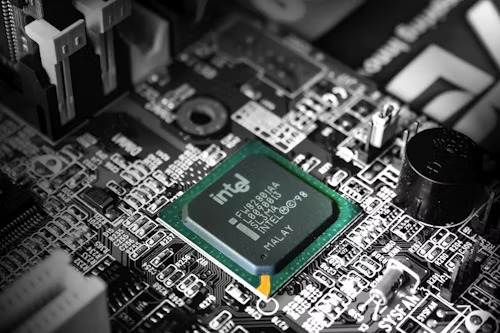
Text

TechnosCOE se start your professional journey with Job-Oriented VLSI Training Institutes in India with Hands-On Practice. Our industry-focused curriculum and practical labs ensure you gain real-world VLSI design skills. Get trained by experts, work on live projects, and secure placement opportunities. TechnosCOE is your gateway to a successful VLSI career in India.
0 notes
Text
Top DFT Training Institutes in Bengaluru for Mastering Scan Insertion
In the rapidly evolving semiconductor industry, Design for Testability (DFT) has become an essential component in ensuring chip reliability. As the complexity of integrated circuits continues to grow, mastering DFT techniques such as scan insertion has become increasingly critical for aspiring chip designers. If you're looking to advance your skills in this specialized field, Bengaluru offers a range of top DFT training institutes tailored for engineers and professionals eager to excel in chip design.
Whether you're a fresh graduate or a seasoned professional seeking to specialize in DFT, selecting the right training program can significantly impact your career trajectory. This post delves into the importance of scan insertion in DFT, the benefits of mastering these techniques, and highlights some of the top DFT training institutes in Bengaluru.
Understanding DFT and Its Importance in Chip Design
Design for Testability (DFT) is a methodology that ensures integrated circuits can be effectively tested after fabrication. As chip designs become more intricate, DFT techniques are crucial in detecting faults early, thereby reducing time-to-market and improving overall product quality.
At the heart of DFT lies techniques like scan insertion, which embeds test features directly into the design, simplifying the testing process and enhancing defect detection capabilities. With the constant demand for higher performance and cost reduction in semiconductor manufacturing, DFT plays a vital role in ensuring chip reliability and minimizing production risks associated with undetected defects.
The Significance of Mastering Scan Insertion Techniques
Mastering scan insertion techniques provides a multitude of benefits in chip design, including:
Enhanced Testability: Scan insertion allows for better identification and rectification of defects during manufacturing.
Improved Fault Coverage: Effective scan insertion ensures that most faults are detected, contributing to higher product reliability.
Streamlined Design Process: Knowledge of scan insertion reduces debugging time, enabling teams to focus more on innovation rather than troubleshooting.
Increased Employability: Professionals with expertise in scan insertion are in high demand, making this skill set highly attractive to employers.
Given the rapid advancement of semiconductor technology, professionals proficient in DFT techniques, especially scan insertion, are highly sought after in the industry.
Top DFT Training Institutes in Bengaluru
Bengaluru is emerging as a key destination for those seeking to specialize in DFT and scan insertion. The city is home to several leading training institutes that offer industry-relevant courses in VLSI design and DFT techniques. Here are some of the top training institutes that can help you build expertise in this area:
1. Semicon TechnoLabs Pvt. Ltd.
Semicon TechnoLabs is a renowned name in the VLSI training landscape, known for offering comprehensive DFT courses. They focus on practical training, with hands-on sessions that cover everything from basic DFT concepts to advanced scan insertion techniques. Their collaboration with industry leaders ensures students are exposed to the latest trends and technologies in semiconductor design.
2. VLSI Academy
VLSI Academy offers specialized training in DFT, with a curriculum designed to equip students with in-depth knowledge of scan insertion, fault modeling, and ATPG (Automatic Test Pattern Generation). The academy provides both theoretical and practical learning experiences to ensure a thorough understanding of DFT concepts.
3. GITAM University - VLSI & Embedded Systems Training
GITAM University’s VLSI & Embedded Systems training program is another excellent choice for aspiring DFT professionals. They offer a structured curriculum that covers DFT fundamentals and advanced topics like scan insertion and test strategies, ensuring students are well-prepared for the challenges of modern chip design.
Course Details and Curriculum
DFT training programs in Bengaluru are typically well-structured, with courses that cover both foundational concepts and advanced topics. Most programs include:
Introduction to DFT: Core concepts like scan insertion, fault modeling, and ATPG.
Hands-on Sessions: Practical training using industry-standard tools and software.
Advanced Topics: Fault modeling, scan chain design, and ATPG techniques.
Project Work: Students work on real-world case studies, reinforcing theoretical knowledge and building a strong portfolio.
These programs are designed to ensure that students are equipped with the necessary skills to apply DFT techniques in real-world scenarios, making them job-ready upon completion.
Job Opportunities and Salary Expectations
The demand for skilled DFT professionals is on the rise, with many semiconductor companies and electronics manufacturers actively seeking experts in DFT techniques. Common job roles for DFT professionals include:
DFT Engineer
Test Engineer
VLSI Design Engineer
The salary prospects for DFT professionals are competitive, with entry-level positions offering salaries in the range of ₹4-6 LPA. Mid-level professionals with experience can earn between ₹8-12 LPA, while senior-level experts can command salaries exceeding ₹15 LPA, reflecting the high value employers place on DFT expertise.
Conclusion
Investing in a quality DFT training program in Bengaluru is a strategic decision for anyone looking to pursue a career in chip design. With a focus on practical learning and industry-relevant knowledge, top institutes like Semicon TechnoLabs, VLSI Academy, and GITAM University provide the skills and experience necessary to excel in the field of DFT. As demand for professionals with DFT expertise continues to grow, mastering these techniques will position you for success in the competitive semiconductor industry.
#Best VLSI training institutes in Hyderabad#Top Best VLSI training institutes in Bengaluru#famous DFT training institutes in Hyderabad#Top most VLSI training institutes in Bengaluru
0 notes
Text
Join Cranes Varsity, the leading VLSI training institute in Bangalore. Gain expert knowledge, hands-on experience, and industry-ready skills. Enroll now for top-notch training with placement assistance.
0 notes
Text
Excelling in VLSI: Choosing the Best Training Institute in Hyderabad
Use the online course offered by Takshila-vlsi.com to explore the world of VLSI design. Acquire useful skills and knowledge from professionals to propel your career forward. Enrol right now!
vlsi design course online
0 notes
Text
VLSI Training Institute In Bangalore
Unlock the potential of VLSI technology with Cranes Varsity, the premier VLSI training institute in Bangalore. Gain expertise in designing cutting-edge integrated circuits with our industry-focused curriculum and hands-on training. Accelerate your career in the booming semiconductor industry. Enroll now.
0 notes
Text
Best VLSI Training Institute (Courses) in Hyderabad | Maven Silicon
Join VLSI Course in Hyderabad at Maven Silicon. We are the best VLSI training institutes in Hyderabad, offer in VLSI Design, VLSI Course, System Verilog, UVM, Verilog & ASIC Verification courses. 100% placement assistance, Free Internship!
0 notes
Text
Job oriented vlsi training institute in Hyderabad | Best vlsi institute in Hyderabad
Hyderabad, often referred to as India's "Silicon Valley," has earned its reputation as a hub for technology and innovation. With the city's thriving IT sector and a surge in semiconductor industry demand, Hyderabad has also become a prominent center for VLSI (Very Large Scale Integration) education and training. This article explores the government VLSI training institutes in Hyderabad, delves into the VLSI course fees, and highlights the top VLSI coaching centers and institutes in the city.
Government VLSI Training Institutes in Hyderabad
Jawaharlal Nehru Technological University (JNTU), Hyderabad:
JNTU Hyderabad offers a comprehensive VLSI design course as part of its B.Tech and M.Tech programs in Electronics and Communication Engineering. The university's affiliation with leading semiconductor companies ensures industry-relevant training.
Osmania University:
Osmania University provides specialized courses in VLSI and Embedded Systems through its College of Engineering. These programs are designed to equip students with practical skills required in the semiconductor industry.
VLSI Course Fee in Hyderabad
The course fees for VLSI programs in Hyderabad can vary depending on the institute, course duration, and level of specialization. Generally, government institutes offer more affordable options compared to private ones. Here's a rough estimate of VLSI course fees:
Government Institutes:
Courses at government institutes like JNTU and Osmania University typically range from INR 20,000 to INR 50,000 for M.Tech programs. B.Tech courses may have lower fees.
Private Institutes and Coaching Centers:
Private VLSI coaching centers can charge anywhere from INR 50,000 to INR 2,00,000 for specialized courses.
VLSI Coaching in Hyderabad
Hyderabad boasts a plethora of VLSI coaching centers catering to both students and professionals looking to enhance their skills in VLSI design. Some notable coaching centers in the city include:
VLSI Guru:
Known for its comprehensive VLSI courses and expert faculty, VLSI Guru has earned a reputation for producing skilled VLSI professionals.
Tech Trunk Ventures:
Tech Trunk Ventures offers specialized training in VLSI design, verification, and FPGA design, making it a preferred choice among aspiring engineers.
Online VLSI Courses in Hyderabad
For those seeking flexibility and convenience, online VLSI courses in Hyderabad are becoming increasingly popular. Institutes like VLSI Guru and Udemy offer online VLSI courses that cater to different skill levels and schedules.
Top VLSI Institutes in Hyderabad
Indian Institute of Technology (IIT) Hyderabad:
IIT Hyderabad is renowned for its high-quality VLSI courses and cutting-edge research facilities. It ranks among the top institutes for VLSI education in India.
International Institute of Information Technology (IIIT) Hyderabad:
IIIT Hyderabad offers specialized courses in VLSI and semiconductor design, with a focus on research and industry collaborations.
Conclusion
Hyderabad's vibrant tech ecosystem, coupled with the presence of government VLSI training institutes and private coaching centers, makes it an ideal destination for pursuing VLSI education and training. Whether you're looking for affordable government programs or seeking specialized courses at private institutes, Hyderabad has options to suit your needs. Additionally, online courses provide flexibility for learners looking to enhance their VLSI skills from the comfort of their homes. With its reputation for innovation and technology, Hyderabad continues to nurture the aspirations of future VLSI professionals.
0 notes
Text
Online Vlsi Training Institutes | Takshila-vlsi.com
Visit takshila-vlsi.com to find out which VLSI schools are the best. Gaining hands-on experience can propel your VLSI design career to new heights.
online vlsi training institutes
0 notes
Text

Your Path to Success Starts at the Best VLSI Training Institute in India
TechnosCOE se Start Your Path to Success Starts at the Best VLSI Training Institute in India. Designed for aspiring engineers, our courses prepare you for top semiconductor careers. Unlock your potential and lead the future of chip design. Start your journey today with TechnosCOE!
0 notes
Text
Mastering VLSI from Home: The Rise of ASIC and Verification Training Online
The Growing Importance of VLSI Training in the Digital Era In today’s rapidly evolving electronics industry, the demand for specialized VLSI professionals is at an all-time high. With industries embracing automation, AI, and IoT technologies, the need for advanced chip design and verification has grown significantly. VLSI (Very-Large-Scale Integration) engineers play a critical role in designing complex integrated circuits that power everyday devices—from smartphones to high-end servers. However, acquiring the right skills to meet industry standards can be a challenge without proper training. Fortunately, online learning has become a reliable gateway to meet this demand through structured, accessible, and high-quality programs.
Learning ASIC Design Through Trusted Online Platforms ASIC (Application-Specific Integrated Circuit) design is a core part of modern chip engineering. It involves creating custom circuits tailored for specific functions, making it an essential skill for any VLSI engineer. As industries continue to prioritize efficiency and cost-effectiveness, ASIC-based systems are becoming increasingly popular. Hyderabad has emerged as a strong hub for VLSI education, and learners now have the convenience of accessing online asic design training institutes in hyderabad These institutes offer interactive sessions, real-time project work, and guidance from industry experts, all from the comfort of home. The right training can open doors to highly lucrative careers in semiconductor design and embedded systems.
Why Online VLSI Education is Gaining Momentum Online VLSI education offers several advantages. Learners can pursue training alongside existing commitments, access recorded sessions for revision, and interact with mentors virtually. Additionally, online platforms often provide up-to-date curriculum designed in collaboration with industry experts. This format suits working professionals, graduates, and students aiming to gain relevant skills without the need to relocate or pause their careers. It also enables access to a wider pool of expertise and networking opportunities, which are essential in a competitive field like VLSI.
Design Verification: The Backbone of Reliable Chip Functionality While designing a chip is important, ensuring its functionality and performance through thorough verification is equally critical. Design verification checks whether the design meets the intended specifications and behaves as expected in real-world applications. As chip complexity increases, verification becomes more challenging and crucial. To meet this demand, several institutes now offer online design verification training programs. These programs teach advanced techniques in simulation, formal verification, and coverage analysis using industry-standard tools. They are specifically structured to prepare learners for job roles such as Verification Engineer and Functional Analyst.
Conclusion: Choosing the Right Path in VLSI Education Pursuing specialized skills in VLSI through online learning is no longer just an alternative—it’s a strategic advantage. With high demand in sectors like consumer electronics, automotive, and telecommunications, training in ASIC design and verification is a smart investment. The presence of reputed platforms like Takshila Institute of VLSI Technologies has made it easier for learners to access quality education remotely. Whether exploring online asic design training institutes in hyderabad or opting for online design verification training, the right course can pave the way for a rewarding career in the semiconductor industry.
0 notes
Text
VLSI Training Institute in Bangalore
Advance your career with Cranes Varsity, the leading VLSI Training Institute in Bangalore. Expert faculty, industry-relevant curriculum, and placement support. Enroll today!
0 notes
Text
Master the Future of Chip Design with Expert Physical Design Courses in Hyderabad
The Booming Demand for Physical Design in VLSI
The digital revolution has transformed how the world functions, and behind every electronic device lies a complex microchip designed through a meticulous process. One of the most critical stages in chip creation is physical design, which directly impacts a chip's speed, power, and area. As technology nodes shrink and semiconductor complexity rises, skilled professionals in this domain are in high demand. Hyderabad, a major hub for the semiconductor industry, is now emerging as a preferred location for learning VLSI physical design, offering specialized and flexible training programs.
Online Learning Options for Busy Learners
In today’s fast-paced world, not everyone can attend full-time classroom training. Recognizing this, many reputed institutions now offer flexible and interactive learning formats. The online physical design course in hyderabad is becoming a popular choice among both fresh graduates and working professionals. These courses provide access to expert trainers, industry-standard tools, and real-time project exposure, all from the comfort of home. Online platforms also make it easier for learners to balance their job, education, and personal commitments, making high-quality education more accessible.
Significance of Physical Design in VLSI
Physical design is a vital step in the VLSI design flow where the logical design is translated into a physical layout. It involves floorplanning, placement, clock tree synthesis, routing, and design rule checks. Every step must meet performance requirements while ensuring minimal power consumption and area usage. Mastery in this area opens up career opportunities in companies that design chips for smartphones, computers, networking systems, and more. Understanding physical design is not just beneficial; it is essential for anyone aiming to build a future in VLSI.
Choosing the Right Training Path
The selection of a training program plays a major role in shaping a learner’s career in VLSI. Ideal training institutes not only provide theoretical knowledge but also offer real-world application through lab sessions and live projects. Course content must align with the latest industrial practices to ensure that learners gain up-to-date and job-relevant skills. Mentorship and placement support further enhance the effectiveness of the training.
Why Hyderabad Stands Out for VLSI Physical Design Training
Hyderabad has emerged as a prominent center for semiconductor companies, making it an ideal location for training and employment in the VLSI sector. Numerous vlsi physical design training institutes in hyderabad have gained recognition for their structured curriculum and experienced faculty. These institutes provide an excellent learning ecosystem backed by strong industry connections. Completing a physical design course in this city increases the chances of securing placement in well-known chip design companies.
Conclusion
With the rising importance of physical design in modern chip development, gaining expertise in this field can significantly enhance career prospects. Flexible options like the online physical design course in hyderabad are helping learners stay ahead of the curve. In particular, Takshila Institute of VLSI Technologies offers industry-relevant training programs designed to equip individuals with practical knowledge and professional skills. For those looking to make a mark in the semiconductor industry, vlsi physical design training institutes in hyderabad offer the perfect platform to begin a rewarding journey in chip design.
0 notes
Text
Excelling in VLSI: Choosing the Best Training Institute in Hyderabad
One of the best training centres in Hyderabad, Takshila-vlsi.com, will help you realise your full potential in VLSI. Get practical experience to further your career.
top vlsi training institutes in hyderabad
0 notes
Text
VLSI Training Institute in Bangalore
Discover top-notch VLSI training at Cranes Varsity, the leading VLSI training institute in Bangalore. Elevate your skills with our comprehensive VLSI courses, designed to empower you with cutting-edge knowledge and hands-on experience. Join us to unlock a world of opportunities in the field of Very Large Scale Integration. Enroll now for expert-led VLSI training at Cranes Varsity, your gateway to a successful career in semiconductor technology.
0 notes
Text
Best VLSI Training Institute in Pune | Maven Silicon
Join VLSI Course in Pune at Maven Silicon. We are the best VLSI training institute in Pune. We offer online and offline courses in VLSI Design, System Verilog, UVM, Verilog, ASIC Verification and such. 100% placement assistance, 24/7 Lab Access and support!
0 notes
Text
final year vlsi project centers chennai
Chennai is a major educational hub offering several specialized institutes that provide expert training and project support for students pursuing VLSI design projects in their final year. These centers focus on delivering hands-on experience with the latest VLSI tools and technologies to help students build a strong foundation for their careers.
0 notes