
It’s more interesting inside than outside. We are fascinated by teardown different things to get to know them better.
Don't wanna be here? Send us removal request.
Statistics
We looked inside some of the posts by teardownit and here's what we found interesting.
Average Info
Notes Per Post
0
Likes Per Post
0
Reblog Per Post
0
Reply Per Post
0
Time Between Posts
11 days
Number of Posts By Type
Text
17
Last Seen Tumblr Blogs


Fun Fact
There were a total of 171.5 billion posts on Tumblr in 2019.
Text
Matrix Connection: Few Pins, Many Options

4+4=8, 4×4=16. It often happens that a microcontroller or other chip has too few pins. You can use a more complex and expensive microcontroller, or you can multiplex the pins. Today I will describe one of the ways to do this.
In previous posts, we have already talked about decoders and demultiplexers, as well as shift registers.
In the first case, an n-bit binary number can point to one of the decoder outputs, the number of which is equal to two to the power of n.
For example, the 74HC138 3:8 demultiplexer chip allows you to light up eight LEDs or turn on eight relays using only three microcontroller pins or three communication wires between devices.

However, this scheme does not allow activating several outputs simultaneously. In the case of LEDs, we can take advantage of the persistence of human vision and constantly send different numbers to the inputs of the 74HC138. If the frequency of numbers changing exceeds 24 hertz, then it will seem to us that from 0 to 8 LEDs are lit simultaneously and continuously.
It should be noted that the more LEDs are used, the dimmer each of them will be. Although in some cases this is a good thing, the consistency of the overall brightness means that when more LEDs are turned on, they will not be blinding.
It is also possible to turn on several relays simultaneously through a decoder, although it is more difficult. Timing circuits similar to those used in running lights with slowly dimming LEDs will be required.

Thanks to diodes with RC circuits at the bases of transistors, relay coils connected instead of LEDs will switch off not at the same moment as the signal disappears from the decoder output but after a certain period of time.
If you keep the capacitor charged by periodically applying the corresponding number to the decoder input, the relay remains on. If you stop transmitting this number, the relay will turn off.
This is very similar to the operation of the Williams-Kilburn tube, one of the first types of computer memory in history. The electron beam scanned the cathode-ray tube screen, just like a television.

To turn the indicator into a storage device, engineers simply added a matrix of electrodes onto the screen and synchronized the modulation of the beam with the scanning of this matrix. Those areas of the glass where the electrons hit acquired a charge that would fade if not renewed.
Of course, this was not a fast memory by any stretch. And controlling a relay via an RC chain is also not fast. However, it fits a number of applications.
Each additional wire or microcontroller pin doubles the capacity of the demultiplexer. For example, 4 bits give 16 outputs. But the required number of decoder chips also doubles. For 4:16 you need two 3:8 chips, for 5:32 you need four, and for 6:64 as many as eight, and so on.

But the shift register allows you to transmit or read practically an unlimited number of binary bits using only three wires: one for data, one for clocking, and one for register latching.

Therefore, when paired with microcontrollers, to expand the number of pins, shift registers are most often used rather than demultiplexers.
Two CD4017 decimal counter-decoders have 2×10=20 outputs. But if you make a matrix where one chip scans the rows and the second the columns, you get 10×10=100. Or 9×9=81, as done in this matrix LED effect.

The same design is used in an electronic timer, where 6×10=60 LEDs are placed around the circumference of the dial and serve as the second hand.

As you can see, the matrix is not necessarily square or rectangular. It can be stretched into a line or closed into a circle, and in general, its elements can be arranged in the shape you need.

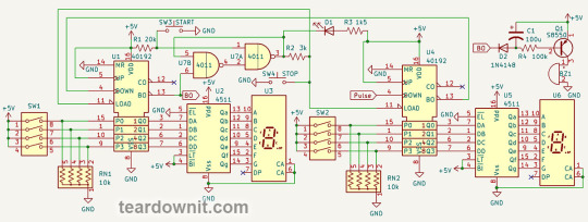
The decade counter U2 receives timing signals with a frequency of 1 hertz from the generator on the 555 timer. Using switch SW1, you can switch the chip to 'disable counting' mode, which means a pause in the stopwatch operation.
U2 counts to ten (from Q0 to Q9) and transmits the CARRY-OUT signal to the clock input of U1. Note that CARRY-OUT goes to logical zero when the counter has counted to Q5, and to logical one at the moment of overflow, when Q0 is activated again after Q9.

The CD4017 chip reacts just to the transition from low to high, so U1 will turn on the next row of LEDs exactly when U2 has turned off column Q9 and turned on Q0.
The active voltage level at the outputs Q0..Q9 of the CD4017 counter is high, and the current in the LED should flow from plus to minus, from anode to cathode, in the direction of the arrow. Therefore, the signals from the U2 outputs are inverted by the U3 CD4069 chip.
This chip contains six logic inverters. To count 60=10×6 seconds, we just need 6 lines of 10 LEDs. On the diagram, they look like rows and columns, but on the board, they are placed around the circumference of the dial.
After a minute has passed and Q2 has counted to Q6, transistor Q1 opens through resistor R2, performing two actions in our circuit.
First, it charges the capacitor C1, the voltage across which turns on transistor Q2 through resistor R3. This is exactly the same scheme that we've discussed above.
While C1 is discharging, the BZ1 buzzer will beep, not continuously but in 1 hertz pulses, since the positive terminal of BZ1 is connected not to the positive power supply terminal but to the output of the second pulse generator.
An asymmetrical flip-flop is constructed on transistors Q3 and Q4. A logical one from capacitor C1 through diode D1 and resistor R4, or from the power supply positive through R5 and button SW3, sets the flip-flop to one, which goes to the reset input of both counters, stopping the counting and resetting them to zero.
The diode is needed so that the buzzer is triggered only at the end of the count, not when the STOP button is pressed or a logical one appears at the output of the trigger through resistor R6, which latches the trigger into a high- or low-level state.
Button SW2 resets the trigger and starts the second count. If you made a multi-position switch that allowed you to choose which of the Q1..Q6 pins to connect R2 to, the timer could count not only up to 60 but also up to 10, 20, 30, 40, and 50 seconds.
And the last circuit for today is an RGB running light. Here IC1 is the familiar CD4060 binary counter, and 74HC138 is a 3:8 decoder that lights up one of the eight LEDs, LED1..LED8.

These are RGB LEDs, and the light color will depend on the state of the outputs Q8–Q10 of the IC1 chip.
000: white; all channels are on
001: blue-green
010: magenta; blue plus red
011: blue
100: yellow; red plus green
101: green
110: red
111: LEDs do not light up
As you can see, even to control RGB LEDs, it is not at all necessary to use a microcontroller. With two simple chips and three transistors, you can create the beautiful effect of a running, color-changing light.
0 notes
Text
Telecommunication Protocols Overview: VoIP
Revolutionary Transition from TDM to IP Networks Voice over IP (VoIP) technology VoIP and Triple Play: Key Protocols for Multimedia Transmission in IP Networks
Voice-over-IP (VoIP), also known as IP telephony, connects TDM networks with channel switching to IP networks with packet switching. It also facilitates the gradual transition from TDM to IP networks. Introduced in the late **1990s**, VoIP is one of the earliest telecommunication technologies to enable the use of IP phones, IP PBXs, and similar equipment; the suite of VoIP protocols is **crucial** among other telecom protocols.
According to the common definition, IP telephony is real-time voice signal transmission over a packet-switched network. It converts a phone number into an IP address and the analog voice signal into a digital one.
The birth year of Internet telephony is considered to be 1995, when Vocaltec released the Internet Phone software for telephone transmission using the IP protocol. **Until** the mid-1990s, Internet phone network implementation was possible only via telephone modems, resulting in significantly lower voice quality compared to traditional phones. Nevertheless, this laid the foundation for VoIP.
Since then, the development has been so rapid that VoIP's capabilities now far exceed its formal name. Essentially, this technology allows for the transmission of not only voice but any type of information using the IP protocol, so the term shifted to a broader one, "multimedia." Corresponding data structures can include voice, images, and data in any combination, commonly referred to as Triple Play.
The VoIP network structure can be viewed as two planes. The lower one represents the transport mechanism for non-guaranteed delivery of multimedia traffic as a protocol hierarchy (RTP, UDP/IP), and the upper one is the call service management mechanism. The key protocols here are H.323 ITU-T, SIP, MGCP, and MEGACO, each offering different implementations for call **services** in IP telephony networks.
Real-time Transport Protocol (RTP) provides transport services to multimedia applications, but it doesn't guarantee delivery or packet order. RTP helps **apps** detect packet loss or order issues by assigning a number to each packet. RTP works in point-to-point or point-to-multipoint modes with no regard to the transport mechanism, but usually it is UDP.
RTP works with the Real-Time Control Protocol (RTCP), which manages data flow and checks for channel overload. RTP session participants periodically exchange RTCP packets with statistical data (number of packets sent, lost, etc.), which senders can use to adjust transmission speed and load type dynamically.
Recommendation H.323
The recommendation H.323, historically the first method for making calls in an IP network, involves the following types of data exchange: - Digital audio - Digital video - Data (file/image sharing) - Connection management (communicating function support, logical channel management) - Session and connection establishment and termination
Key H.323 network elements include terminals, gateways, gatekeepers, and Multipoint Control Units (MCU).
A terminal provides real-time communication with another H.323 terminal, gateway, or MCU.
Gateways connect H.323 terminals with different network protocol terminals by converting the information back and forth between networks.
Gatekeepers participate in managing connections by converting phone numbers to IP addresses and **vice versa**.
Another element of the H.323 network, the proxy server, operates at the application level to identify application types and establish necessary connections.
The H.323 call service plane includes three main protocols (see picture): RAS (Registration Admission and Status) for terminal registration and resource access control, H.225 for connection management, and H.245 for logical channel management. RAS uses UDP, while H.225 and H.245 use TCP for guaranteed information delivery. UDP's delivery is not guaranteed, so if confirmation isn't received in time, UDP retransmits the message.

Pic. 1. Overview of H.323
The process of establishing a connection involves three stages. The first one is to detect the gatekeeper, register terminals with the gatekeeper, and control **terminals'** access to network resources using the RAS protocol. The next two stages involve H.225 signaling and H.245 control message exchanges.
Recommendation H.225 outlines the procedures for connection management in H.323 networks using a set of signal messages from the ITU-T's Q.931 recommendation.
Recommendation H.245 describes the procedures for managing information channels: determining the master and slave devices, communicating terminal capabilities, and opening and closing unidirectional and bidirectional channels. It also covers delays, information processing modes, and the state of information channels by organizing loops.
The exchange of signaling messages between interacting H.323 network devices happens over H.245 logical channels. The zero logical channel, which carries control messages, must remain open for the entire duration of the connection.
SIP (Session Initiation Protocol)
The second method for handling calls in VoIP networks involves using the Session Initiation Protocol (SIP), specified in RFC 2543 by the IETF. As an application-level protocol, it is designed for organizing multimedia conferences, distributing multimedia information, and setting up phone connections. SIP is less suited for interaction with PSTN but is easier to implement. It's more suitable for ISPs offering IP telephony services as part of their package.
Key features of SIP include user mobility support, network scalability, the ability to add new functions, integration with the existing Internet protocol stack, interaction with other signaling protocols (e.g., H.323), enabling VoIP users to access intelligent network services, and independence from transport technologies.
It's worth noting that user mobility support is no longer exclusively a SIP feature. H.323 now also supports it (see ITU-T H.510, "Mobility for H.323 Multimedia Systems and Services").
A SIP network contains user agents, or SIP clients, proxy servers, and redirect servers.
User agents are terminal equipment applications that include a client (User Agent Client, UAC) and a server (User Agent Server, UAS). The UAC initiates the service request, while the UAS acts as the calling party.
The proxy server combines UAC and UAS functions. It interprets and, if necessary, rewrites request headers before sending them to other servers.
The redirect server determines the location of the called subscriber and informs the calling user.
MGCP (Media Gateway Control Protocol)
The third method for building an IP telephony network relies on the Media Gateway Control Protocol (MGCP), proposed by the IETF's MEGACO workgroup. The architecture of this protocol is probably the simplest of all three in terms of functionality. An MGCP network contains a media gateway (MG) for converting voice data between PSTN and IP telephony networks, a signaling gateway (SG) for processing signaling information, and a call agent (similar to an H.323 gatekeeper) for managing gateways.
Like H.323, MGCP is convenient for organizing PSTN-compatible IP telephony networks. However, in terms of functionality, MGCP surpasses H.323. For example, an MGCP call agent supports SS7 signaling and transparent transmission of signaling information over the IP telephony network. In contrast, H.323 networks require any signaling information to be converted by a gateway into H.225 (Q.931) messages. MGCP messages are transmitted in plain text format.
The fourth method for building an IP network, an improvement over MGCP, was developed by the IETF's MEGACO group together with ITU-T's SG 16, hence the name MEGACO/H.248. It mainly differs from its older sibling in connection organization. Thanks to this, the MEGACO/H.248 controller can change the port connection topology, allowing for flexible conference management. The MEGACO protocol supports two methods of binary encoding.
MGCP has also evolved in the field of the Internet of Things (IoT), where it is used to manage media gateways and transmit voice information in various scenarios, such as smart homes or intelligent buildings.
0 notes
Text
Counting pulses and seconds without MCU
Counting pulses, whether time intervals or signals from sensors, buttons, and encoders, is often required. Today, I will describe how to count pulses forward and backward using digital chips.
Counting forward Our first example is a stopwatch that counts to 30 or 60 seconds.

This is just a part of the electronic clock circuit we have assembled.

In the standard use case, half of the CD4518 dual binary decimal counter counts pulses arriving at the CLK input from 1 to 9 and then resets to 0.
Unlike the MC14553B used to make the frequency counter, the CD4518 has no separate output for the overflow signal or for shifting to the higher bit.

Yet, besides the CLOCK input, there is an ENABLE input. Any one of those can be used for clocking.

If the ENABLE input is logical, then the counter value will increment when the CLOCK input goes from low to high. This is the standard way to clock the counter.

The same thing will happen when the ENABLE input transitions from high to low if the CLOCK input is logic zero. This is exactly what happens to the Q4 most significant bit of the U1B counter during self-reset, from 9 = 0b1001 to 0 = 0b0000. Having received this signal at the ENABLE input, counter U1A increments its value.
In an electronic clock, seconds and minutes are always counted from 0 to 59, and at 60, the most significant bit is reset, and the pulse is transferred to the next counter in minutes or hours.
And our stopwatch can count up to both 60 and 30 seconds. In the first case, counter U1A should count to 6 = 0b0110, and in the second, to 3 = 0b0011. One can switch this stop condition using the S1 switch, made as a jumper.
When the specified number of seconds is reached, the counters are not reset. Instead, a logic zero is applied to the ENABLE U1B input, which denies pulse counting. If one completely removes the jumper, the counting will also stop.
The SW1 button is used to reset the counters, supplying high logical levels to the designated inputs of U1A and U1B. While it is pressed, both counters stay at zero even though the clock generator continues to send pulses every second.
The pulse generator is made according to a circuit that is very familiar to us at this point on the NE555D timer. It does not have quartz stabilization, but its accuracy is acceptable for a training model or kitchen timer.
At a higher supply voltage, timing capacitor C2 will be charged through R6 and R5 with a higher current. But thanks to the voltage divider of three 5 kOhm resistors built into the 555 chip, the thresholds for switching the charge and discharge modes of the capacitor will rise accordingly.

Thanks to the design of the 555 timer, the frequency of the second pulse does not depend on the circuit's supply voltage. This is why the 555 timer is called a precision one.
Counting back The second version of the stopwatch also uses a clock generator on a 555 timer and CD4511 binary decimal decoders. But unlike the first one, it can count backward not from one of two fixed values but from any number of seconds in the range of 0 to 99.

Remember the post about flip-flops? One such flip-flop is assembled on two NAND gates of the CD4011 chip. If you press the START (SW3) button, logical zero will appear at input 1 of U7A.
Accordingly, output 3 will have a logical one, regardless of the state of input 2. After all, 0 AND X = 0, and NOT (0 AND X) = 1.
Through the resistor R2, this logical one from the output of the flip-flop is supplied to the ¬LOAD inputs of both CD40192 chips. This switches them from direct value loading mode to counting mode.
From the output of the same generator used in the first stopwatch on the NE555 (therefore, not shown in the diagram), second pulses are sent to the DOWN clock input of the U4 chip.
The generator has a pause button shunts the timing capacitor to the ground. While it is pressed, second pulses are not sent. Sending resumes when one releases the pause button.
U4 counts decremental until it reaches zero. At this moment, the chip supplies a logical zero to the borrow output BO, which then goes to the U1 clocking DOWN input—the high-register counter.

The next second pulse resets U4 to 9 (and not to 15 since the CD40192 is a BCD counter, unlike the purely binary CD40193). At the same time, the U4 BORROW output and, accordingly, the U1 decremental input go into a high logic-level state. Just at this moment, U1 counts down one second.
When U1 reaches zero, logic zero from its BORROW OUT will go to input 6 of logic gate U7B. At output 4, there will be NOT (1 AND 0) = 1, and accordingly, NOT (1 AND 1) = 0 at output 3 of U7A.
Logical zero at the ¬LOAD inputs will switch CD40192 chips from counting mode to direct value loading mode from microswitches SW1 and SW2.
At the same time, a low logic level at output 3 of U7A will cause LED D1 to light up and open PNP transistor Q1, which is connected to a common-emitter circuit. Buzzer BZ1 will go off.
The LED will stay lit, and the buzzer will beep until the SW3 START button is pressed again or the power is off.
Q1's base current is limited by R4 to less than one milliamp, and D1's LED current is limited by R3 to just over two milliamps.
If we were to turn on the buzzer BZ1 between the power supply positive and the emitter of transistor Q1, connecting the collector to the ground, we would get a circuit with a common collector that can limit the base current on its own. Then, it would be possible to do without R4, thereby saving ourselves one resistor.
Personally, I don’t like the buzzer beeping obnoxiously all the time when the countdown is not running. This would be exactly what you need for any speed competition. But in all the other cases, for the buzzer to go silent, you must turn off the power to the stopwatch or do two additional things: restart the countdown and pause the second pulse generator. So uncomfortable.
To make the buzzer sound for a limited time after the end of the countdown, one can use a monostable circuit on a 555 timer or an even simpler circuit from the post about decoders and demultiplexers.

This circuit ensures that a pair of LEDs light up and gradually fade to zero as capacitor C3 discharges. Our stopwatch will look like this:
0 notes
Text
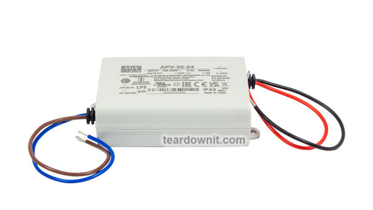
Review, teardown, and testing of APV-35-24 Mean Well power supply


Click image to zoom
General Description
Brief Specification: APV-35-24 is a power supply unit with an output voltage of 24 volts DC and a current up to 1.5 amperes. According to the specifications, the PSU has an extended operating range for input AC voltage from 90 to 264 V. When input voltage decreases from 100 V to 90 V, the supported load power decreases linearly from 100% to 80% of the nominal rating.
This power supply can also operate on a DC network within a range of 127 to 370 V.
The unit’s dimensions are approximately 3.3 x 2.2 x 1.2 inches (exactly 84 x 57 x 29.5 mm). It has a neat, tactile, light gray plastic casing, presumably made of ABS. The casing appears solid and unrepairable (or hides its secret).

The PSU lacks external indicators, output voltage, or current adjustments. It does not have power factor correction (PFC) and offers an efficiency of around 84%. While it has overload and output overvoltage protection, it lacks thermal protection.
Test Conditions
Most tests were conducted using Test Circuit 1 (see appendix) at 80°F (27°C), 70% humidity, and 29.8 inHg atmospheric pressure.
Unless specified otherwise, measurements were taken without pre-warming the power supply in a short-term load mode. Input voltage was set at 115V AC, and 1.5 A was considered 100% load.
To determine load level, the following values were used:

Static Load Output Voltage

The change in output voltage with load changes did not exceed 0.7%.
Startup Characteristics
Power-On at 100% Load
The unit was kept off for at least 5 minutes with a 100% load connected before the test.
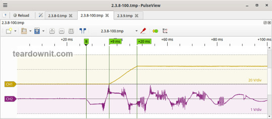
The oscillogram below illustrates the startup process at 100% load (Channel 1: output voltage, Channel 2: input current):

The startup waveform has three phases:
Input current spike to charge capacitors upon power connection, peaking at 7 A, lasting less than half a cycle of the input voltage (5 ms).
Waiting for the control circuit to initialize, approximately 17 ms.
(Output Voltage Rise Time) Voltage increase, taking 7 ms.
(Turn-On Delay Time) The entire startup process takes 24 ms.
(Output Voltage Overshoot) The startup process is aperiodic with no overshoot.
Power-On at 0% Load
Before testing, the unit was kept off for at least 5 minutes with 100% load. Then, the load was disconnected, and power was turned on.
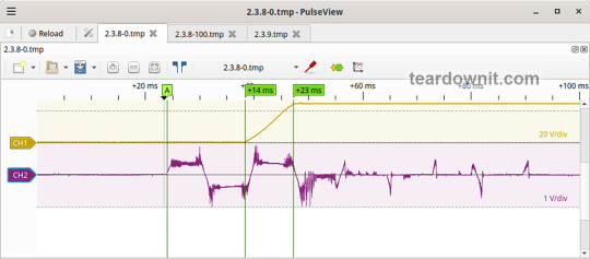
The oscillogram below illustrates the startup at 0% load:

The startup waveform has three phases:
Input current spike to charge capacitors, peaking at 6 A, lasting less than half a cycle (5 ms).
Waiting for control circuit initialization, around 23 ms.
(Output Voltage Rise Time) Converter startup and voltage increase, lasting 6 ms.
(Turn-On Delay Time) The entire startup process takes 29 ms.
(Output Voltage Overshoot) The startup process is aperiodic with no overshoot.
Power-Off Characteristics
Shutdown was conducted at 100% load with nominal input voltage. The oscillogram below illustrates the shutdown process:

The power-off process has two phases:
(Shut Down Hold Up Time) The source continues running on capacitor charge until voltage drops below a critical level, after which nominal output can no longer be maintained. This phase lasts 78 ms.
(Output Voltage Fall Time) Output voltage drops, the converter halts, and the voltage drop accelerates. This phase lasts 27 ms.
(Output Voltage Undershoot) The shutdown is aperiodic with no undershoot.
Peak current at 100% load before shutdown: 1 A.
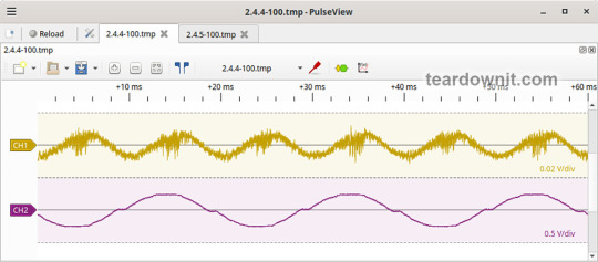
Output Voltage Ripple
100% Load
A low-frequency ripple with an amplitude of approximately 60 mV is observed. The same diagram shows the waveform of the input current (Channel 2) with an amplitude of 1 A.

Both switching frequency (~62 kHz) ripple and noise at 100% load have an amplitude of about 350 mVp-p.

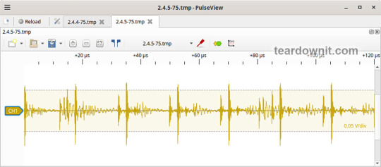
75% Load
Low-frequency ripple at approximately 60 mV with a sin-like waveform; amplitude of input current is 0.75 A.

Switching frequency ripple at 75% load is around 350 mVp-p, switching noise of 450 mVp-p.

50% Load
Low-frequency ripple reduces and appears as noise, masking harmonics at grid frequencies, around 50 mVp-p. Input current peaks at 0.5 A.

Switching ripple at 50% load is 300 mVp-p, and switching noise reaches up to 700-750 mVp-p.

10% Load
Low-frequency ripple appears as noise with an amplitude of 110 mVp-p, masking grid harmonics. Input current peaks at 0.3 A.

Switching ripple is around 200 mVp-p, with noise near 800 mVp-p.
Notable is the change in the converter's operation—specifically, the interval between energy transfer cycles to the load increases from 16 microseconds to approximately 39-41 microseconds. It's unclear what causes this; one might initially assume the converter simply lowers its frequency as the load decreases. However, when running with no load, this interval returns to 16 microseconds. On the other hand, it doesn’t seem to be subharmonic oscillation due to insufficient slope compensation either, as the periods aren’t multiples of each other. It would be helpful to look "under the hood," but the case is too pretty to break open.

0% Load
Current consumption without load is 19 mA, according to the multimeter.
(Power Consumption) Input current in this mode is primarily reactive in nature; thus, the power consumption value could be challenging to measure with simple instruments.
Low-frequency ripple at 0% load is approximately 50 mVp-p. The input current waveform resembles a sinusoid with some noise.

Switching frequency ripple with no load is masked by noise of 200 mVp-p.

Dynamic Characteristics
Dynamic testing involved periodic switching between 50% and 100% load. The oscillogram below illustrates the process:

The oscillogram shows a smooth response to load changes without overshoot, though the load change response reaches 2 V p-p, which is relatively high. Channel 2 shows input current changes in relation to load changes.
Overload Protection
Manufacturer-specified Hiccup Mode protection was verified during testing. In the event of an overload or a short circuit across the output terminals, the power supply switches to a pulsed (hiccup) mode and automatically resumes normal operation once the overload condition is removed.
Overload protection triggers at 2.1 A output current.
Input Circuit Safety Assessment
(Input Discharge) Time constant for input discharge was measured at 0.199 s, resulting in a discharge time of 0.32 s to safe voltage levels (<42 V) when used with 120 V AC.

Important: This result applies only to the tested unit and was obtained exclusively for research purposes. It cannot, under any circumstances, be considered a guarantee of safety.
Thermal Characteristics
No noticable heating of components was observed during no-load operation.
Thermograms were taken at 80%, 90%, and 100% load. At 80% load, the hotspot reached 131.3°F (55.2°C, +28° above ambient). At 90%, it reached 142.5°F (61.4°C, +34°). At 100% load, the maximum temperature was 151.7°F (66.5°C, +40°).
80% load

90% load

100% load

Conclusions
The APV-35-24 is a simple power supply unit with considerable noise and moderate dynamic response and should be used accordingly. It does not reach unsafe temperatures but lacks thermal protection, so it should not be left unattended.
Unfortunately, internal inspection is not possible without destroying the casing.
Important: The results and conclusions presented apply only to the tested unit and were obtained solely for research purposes. Under no circumstances should they be used to assess all devices of this type.
0 notes
Text
How to make a PCB

Today, I will cover in detail and show the process of making a printed circuit board at home. In addition to a soldering iron and a pair of side cutters, you will need a laser printer, an iron, a micro drill, and a few other tools for this job.
I test my designs on traced PCBs and do not use universal prototyping boards. It’s more convenient for me personally, and here’s why.
On the one hand, tracing a PCB takes time. On the other hand, it is also required to carefully arrange components and connections on a universal board. Additionally, you will need to cut traces on a stripboard or, on the contrary, make the traces you need on a breadboard if it is a matrix of pre-drilled holes with separate copper pads.
A board designed in CAD can then be copied in any number, either by making it yourself or by ordering from a factory, all new and shiny, already with a solder mask and silkscreen printing.
Finally, repairing and modifying a circuit on a printed board can be easier than on a universal one. Especially if long pins of the components on a universal board are used as tracks.
So, I drew the scheme in Schematic Editor, part of the KiCad 7.0 software package. This will be a microphone preamp; I will describe it more thoroughly in the upcoming posts. Moreover, this essay is on making the actual board, not its schematics.

Next, one needs to run the footprint assignment tool and specify the footprint for each and every component.

Then, we need to export the netlist.

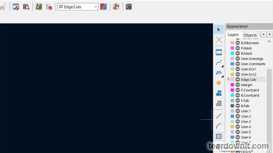
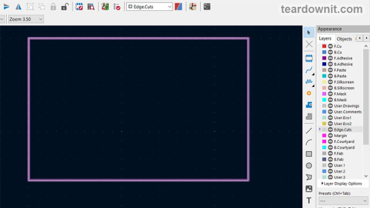
On the Edge. Cuts layer draw a rectangle that specifies the dimensions of our future PCB.
Now, we need to lock that rectangle so that it does not stand out too much and prevent it from being changed while we continue to draw our board layout.
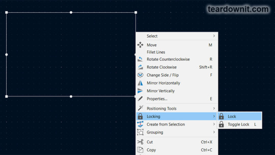
One should ensure the Locked Items checkbox is unchecked on the Selection Filter.
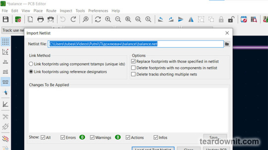
Next, open PCB Editor and import the netlist.

Click Load and Test Netlist, and then Update PCB.
Then, you can place the components and draw the tracks.

We can view a 3D model of the future board at any time.

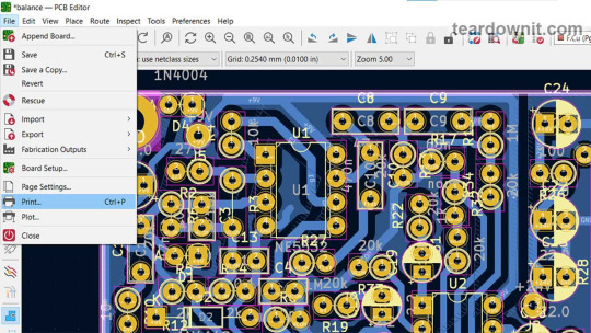
Once all the components are in place and the traces and polygons are drawn, one can print an image of the copper layer. You should turn off the toner save mode on your laser printer.
You can use glossy photo paper (designed for inkjet printing), any pages from glossy ad brochures or magazines, or special heat transfer paper for laser printers from electronics enthusiasts' stores. It is often colored yellow.
My board is single-sided, with all the components on the front side and all the copper on the backside. Therefore, we select the B.Cu and Edge.Cut layers for printing. The print scale should be 1:1.
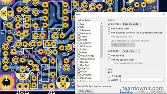
If printing the front copper layer of F.Cu, we need to check the "Print Mirrored" checkbox.
Next, you must cut out a board of the required size from foil fiberglass. Some of us have access to professional cutters or use tin snips.
Others can utilize a rotary power tool with a cutting wheel or even an angle grinder. This is not the best option since fiberglass dust contains microscopic glass particles that irritate the skin and are very harmful if inhaled.
Due to its material, fiberglass PCB quickly dulls any tool except a diamond one. You can see the PCB with a hacksaw, but it will end up its teeth very quickly.
I use an adjustable tile hole cutter for cutting fiberglass. It contains two carbide cutters that can scratch a deep groove in the board and then simply break it along this groove.

These cutters are specifically designed for working on rigid materials, so CEM will not soon dull them. With this technique of cutting the PCB by scraping the track, we minimize the amount of glass dust and do not scatter it in the air.
Next, you need to carefully clean the surface of the copper foil. You can use the finest sandpaper, mild abrasive powder, or steel wool for dish cleaning. I use just a hard eraser. The point of cleaning is not only to remove dirt, oils, and oxides but also to cause micro-scratches for the toner to stick to.
Immediately after, the board must be thoroughly washed to remove any small foreign particles, then fried and degreased with acetone, lighter fluid, ethyl, or isopropyl alcohol.
So, we have a clean, dry fiberglass blank and a piece of glossy paper with traces printed on it. Textolite and paper are the same size. I fold them together and wrap them in a layer of office paper, newspaper, or, better yet, rolling paper.
Thin paper is needed so the glossy paper does not move relative to the PCB. Now, we place the wrapped board blank on a heat-resistant flat surface that we don't mind getting dirty. I use a stack of a few cardboard packaging sheets.
We take the iron, turn it on, and set the temperature as high as it goes. We place it on the blank board and iron it for three to four minutes so the blank has time to warm up nicely.
There is no need to press too hard, but the pressure should be firm. The skill comes with experience. To hold the hot workpiece while ironing, you can use a chopstick.
Remove the iron from the board and turn it off. Remove the wrapping paper from the board after it has cooled off, and place the PCB and the glossy paper in a warm water bath.
Next, slowly and carefully tear off the paper piece by piece from the fiberglass. The tracks and pads on the copper foil should be imprinted.

If some part of the board's design comes off, it can be restored with a permanent marker after the board is completely dry. If a significant piece of the polygon has fallen off, you can just tape it.
Next, I glue strips of tape on the non-foil side of the board to make small hanging rings to hold the board while etching. Throwing a chopstick through these rings is convenient to keep the board hanging. For etching to occur evenly, the board must be swiveled from side to side to mix the solution.

I use a ferric chloride solution for etching, which can be used multiple times. You can store it in a plastic or glass container with a non-metallic lid. This poisonous solution will corrode almost any metal, including stainless steel, so it should be stored, marked, and used cautiously.
To prepare an etching solution, you must take water at room temperature, pour it into a non-metallic container, and add ferric chloride little by little, stirring until the ferric chloride stops dissolving.
The solution will heat up during the dissolution process, not as much as when slaking lime, but noticeably. There is no need to filter the prepared solution or remove the sediment from the bottom of the container.
The optimal temperature for etching the board is 105–130°F (40–55°C). You can heat the solution past that, but then it may wash away permanent marker drawings.
I use plastic food containers for etching and a microwave to heat up the solution. I place the plastic container with the lid loosely closed inside a second bigger one with a lid on and turn on the microwave for one minute. This way, I can be sure that ferric chloride will not damage the microwave.
Once the excess copper on the board has completely dissolved, the board should be immediately washed with plenty of water using a toothbrush. If you do this over a metal sink, be sure not to leave a drop of etching solution anywhere; it can eat right through the sink.

Using acetone, we erased the toner from the washed and dried board and began drilling holes with a microdrill.

Trying the board in the case.

Then, you can begin soldering the components immediately. Still, the best results are obtained if you tin the entire copper foil. I use solder paste for this; just remember that it is toxic, and after working with it, you must wash your hands and wipe the table's surface clean.
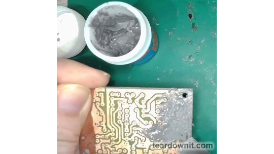
Apply solder paste using a spatula in as thin a layer as possible, as if applying thermal paste to a processor. Next, heat the copper foil with a soldering iron.

Now, wipe or rinse the board with the same degreaser liquid you've used before transferring the toner, and you can place and solder the components.

0 notes
Text
Digital Transmission Systems: Eye Diagram and Bit Error Ratio
Let's take a look and evaluate existing methods for assessing signal quality.
Eye diagram analysis
An eye diagram is a convenient (and ingeniously simple!) graphical method for assessing the quality of a digital signal. It is the result of the superposition of all possible pulse sequences over a period of time equal to two clock intervals of the linear signal.
The simplest example is a diagram for a ternary (logical levels of -1, 0, +1) linear signal with a raised cosine pulse shape of the regenerator input signal. The eye diagram's eye-opening area (or just "opening") is clearly visible, within which the signal identification operation should be carried out for each of the two designated levels. The horizontal lines marked as '-1', '0', and '+1' correspond to the pulse amplitudes with no interference, and the vertical lines at each clock interval T correspond to the correct identification moments.

The decision-making process is represented by two crosses in each "opening" of the eye diagram. The vertical segment of each cross determines the moment of decision, and the horizontal segment represents its level. Error-free regeneration of the digital signal is guaranteed if there is a certain area within the proximity of each cross within which the signal is recognized.
Interference leads to a reduction in this area compared to the ideal case. The minimum distance between the centers of the crosses and the edges of the "eye" serves as a measure of the interference protection margin. The margin decreases due to distortions in the pulse shape and imperfections in the decision-making process. The first reason leads to a decrease in the "opening" of the eye diagram, and the second leads to a movement of the decision point along the edges of the eye. Distortions arising as a result of these two reasons are usually divided into amplitude and time, corresponding to the vertical and horizontal shifts of the decision point. For the convenience of further explanation, we assume that the decision point remains put and the 'opening' decreases.
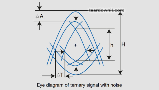
The degree of 'squinting' of the eye diagram is determined by the resulting distortions caused by intersymbol interference, echo signals, changes in the amplitude of pulses at the output of the regenerator, and errors in the thresholds of trigger devices. The result of these influences is ∆A, the vertical component of eye-diagram distortion. It is the value for the edges of the ideal eye diagram to be shifted.
Time distortions of the eye diagram ∆T, including the discrepancy between the decision moments and their static values and jitter, are usually taken into account in the horizontal shift of the "eye" edges.
Obviously, to compensate for the deterioration of the real eye diagram compared to the ideal one, the signal-to-noise ratio must be increased by ∆S/N = 20×lg(H/h) dB, where H and h stand for the vertical "opening" of the ideal and real eye diagram, respectively.
Bit error ratio
The error rate is a key quality parameter in Digital Transmission Systems (DTS). There are many error metrics; let's describe a few. The simplest is the bit error ratio (BER) or jitter, which is relevant for VoIP telephony or inter-network gateways. This is a reminder that BER should be understood as the ratio of corrupt bits to the total number transmitted.
It should be noted that BER depends on the number of bits transmitted. For example, a long sequence of identical symbols can cause low-frequency amplitude modulation and a persistent jitter, resulting in increased errors. Standard test sequences are used to ensure a correct comparison of different transmission systems, and each standard transmission speed has its own test sequence. Their properties are close to Gaussian noise but have a certain loop period. Therefore, they are called not just random but pseudo-random sequences (PRS) or pseudo-random bit sequences (PRBS).
It should be emphasized that the BER estimate will only be absolutely accurate if the number of bits transmitted is infinite. Strictly speaking, when their number is limited, we do not get the probability of an event BER, but its estimate BERT. Surely, the confidence level (CL) of this estimate, also called the confidence interval (CI), depends on the number of errors caught and on the total number of transmitted bits N.
This is confirmed by the data in the table below, which shows the required values of the normalized duration NxBER depending on the number of registered errors E and the confidence level CL of the estimate: the greater the number of registered errors and the confidence level CL of the estimate, the greater the number of bits that must be transmitted.
A typical BER measurement scheme involves a BER tester test bit (character) sequence generator, a test object (regenerator, DTS section, etc.), and a BER tester error detector.
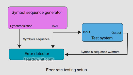
The BER tester generator forms test signals fed to the input of the object under test. The signal generator under test is also the signal source for the error detector of the BER tester.
The tested object can be geographically co-located with the BER tester or be at a remote spot. In any case, the test object must be taken out of service, and the signal from its output must be directed to the receiver input of the BER tester. As telecom specialists call it, a measuring loop must be organized.
The error detector receives a test signal from the output of the object under test or generates an exact copy of this signal autonomously. The generator test signal is compared bit by bit with the signal coming from the object's output under test. The detector records each signal difference as a bit error.
An error detector ensures the necessary in-phase of the two indicated signals by providing the required delay of the signal from the generator output. Signal phasing is usually performed during the calibration of the BER tester.
The test signals of BER testers are standardized. As noted above, the information signal in BER testers is simulated in the form of so-called pseudo-random sequences (PRS or PRBS). They are formed in accordance with standard algorithms and differ in the number of generated symbols M = 2k–1, where k is an integer.
BER tester generators provide the ability to create custom test sequences, usually called codewords.
A clear disadvantage of BER is the need to take the tested object out of service (OoS), which is acceptable when equipping or rebuilding the facility and is inconvenient if the DSL is already in operation. More than that, BER is quite good for assessing the impact of single noise occurrences caused by Gaussian processes, such as self- and transient noise. At the same time, in any real communication system, there are packets of such errors (also called serial errors). Therefore, without knowledge of the time structure of errors in the communication system, it is impossible to effectively localize damage and accumulate adequate information about the quality of the design and installation of equipment. In fact, the BER parameter alone is not enough to correctly assess the performance of a DSL. More adequate quality indicators of DSLs are needed, taking into account the interference structure, with the ability to monitor them during normal operation of the communication system ('In Service Monitoring,' ISM), such as recommendations G.821 and G.826.

Required values of normalized duration
0 notes
Text
The amazing secrets of Krank Distortus Maximus
This distortion pedal has a fascinating history, an unusual circuit design, and great sound. It's hard to believe that just one LM386N3 chip plus two bipolar transistors at the input and output can sound like this, even without clamping diodes!
Yes, that's not a typo. We are used to the fact that the LM386 is a power amplifier chip for headphones or a tiny speaker. But in essence, it is an operational amplifier. It can do a decent job as a part of the overload effect.

Krank Amplifiers is a boutique brand for expensive and rare tube guitar amps that are no longer in production and, therefore, are very desirable and collectible.
Tony Krank started his career as a guitar technician. He has collaborated with star guitarists like Slayer's Kerry King and Metallica's James Hetfield. From repairing amplifiers, Tony naturally moved on to modifying them and then making his own ones.

In 2003, brothers Tony and Kent founded Krank Amps in Tempe, Arizona. Their amplifiers came out as very innovative and unique. Of course, they were intended for the extreme metal and hard rock genres.
The amplifiers had two channels: clean (KLEEN) and cranked (KRANK). If your last name is Krank and you make amps for metal bands, these are the most appropriate names for amp channels!
In fact, the last name of brothers Tony and Kent is Dow. But Tony played for a long time in The Kranks and became known as Tony Krank. So, he passed this surname to the amplifiers.
The Krank channel provides very high gain and a compelling growl sound, mandatory for killer thrash metal riffs.
And the Kleen channel of these amplifiers has no extremes: not too sweet or sparkling. Just what you need for clean-sounding losses in modern progressive metal.
Not all guitarists liked the high-gain sound. Krank amps, like any other, take some getting used to. In particular, it takes some time to achieve such a balance of treble and presence settings to sound musically pleasing both on stage and in recording.
Ten years ago, Krank amps and cabinets were a common sight on stage, but now almost all of them have gone for good. There are several reasons for this.
Firstly, the amplifier design wasn't durable enough to survive a concert tour, and breakdowns occurred quite often.
Secondly, many touring guitarists have started to favor three- and four-channel amps, not to mention those who switched to digital.
Thirdly, and most importantly, many copies of Krank cabinets, heads, and amps have been bought by music producers. These devices were successfully used in studios when there's enough time to set up the best sound; structural strength is low on the priority list, and the quality of recording for thousands of pairs of headphones and speakers is a top goal.
In 2007, Krank introduced two new pedals at NAMM. The first was fine, yet unremarkable, Krankshaft Overdrive. The circuit was just a rip-off from the Ibanez Tube Screamer TS808.

We have a separate post about Tube Screamers and their numerous variations. I think that every guitarist absolutely needs at least one Tube Screamer. It could also be Krankshaft Overdrive: a great-sounding, well-designed, and well-made pedal, just like your average Tube Screamer.
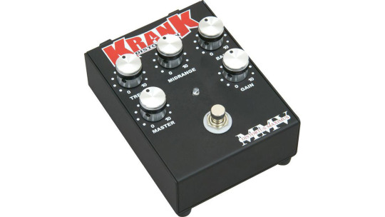
Much more exciting and unique was the second pedal—the Distortus Maximus. With a full three-way tone stack and an authentic Krank high-gain channel sound, this is indeed a pedal everyone should at least try!
Building your own copy is not difficult; the pedal circuit can be called very simple. The guitar signal path begins with the amplifier stage on transistor Q1. This seems to be the most common cascade with a common emitter, but it has a few features affecting the sound.

The BC550C is a low-noise transistor with a high current gain of 420 to 800. Look closer at the resistor values that set its base bias.
Typically, in preamp stages, these ratings are made equal or almost equal so that half the supply voltage is at the base of the transistor, and the stage operates in class A mode with minimal distortion.
There are also circuits with no lower resistor, and the resistance of the upper one is selected so that it provides the desired quiescent currents of the collector and base.
This was often done on battery-powered radios to save battery life. DIY superheterodyne from the post on Regency TR-1 is no exception. All high-, intermediate-, and audio-frequency pre-amplifier stages in the circuit of this receiver are designed exactly like this.

And in the Krank Distortus Maximus circuit, the resistance values in the base circuit are designed to ensure the minimum quiescent current of the cascade. For this reason, they differ tenfold! This results in AB mode, which is very close to pure class B.
In this mode, the imperfections of the already low-noise transistor will be completely minimal, which is crucial for a high-gain amplifier. And also, significant nonlinear distortions will occur, which in this case will give the sound asymmetrical compression, even to the point of slight limitation. And these distortions have a pleasant "tube" tint.

One day, I will try to rebuild the Q2 preamp stage of the BOSS DS-1 according to the design of the first stage of the Distortus Maximus. This should respond more pleasantly to the powerful signal of classic hot-rodded and modern humbuckers.
The LM386 chip in the Distortus Maximus is configured to have maximum gain; pins 1 and 8 are connected. They are also connected to a tone-correcting chain consisting of a 100-ohm resistor and a 47-uF capacitor to ground.

Next, we see a complete three-way tone stack and a seemingly ordinary output buffer made according to an emitter-follower circuit. But this buffer is also unusual.
No lower resistor would set the base voltage of transistor Q2 along with the upper 100 kilo-ohm resistor. Therefore, we have not just a voltage follower but a circuit stage that introduces distortion with a "tube" character into the output signal!
This pedal is, to put it mildly, a circuitry masterpiece. Behind its apparent simplicity lies a deep feel for guitar sound; the design utilizes the nuances of transistors and LM386 operation. The video below captures its actual sound.
This is probably my best homemade distortion pedal to date. It is practically an entire single-channel amplifier in a box. I never cease to be amazed by the sound obtained from such a small pile of simple parts!
0 notes
Text
Review, teardown, and testing of HLG-185H-24A Mean Well power supply
General Description

Brief Specification
The HLG-185H-24A is a power supply unit with a DC output of 24 volts and up to 7.8 amps. According to the specification, this unit has an extended input voltage range for AC power, from 90 to 305V. When the AC input voltage drops from 100 to 90V, the support load power linearly decreases from 100% to 80% of the nominal rating.
This power supply can also operate on DC power within a range of 127 to 431V.
The unit's dimensions are 9 x 2.7 x 1.5 inches (228 x 68 x 38.8 mm). The casing is made of aluminum profile, sealed with compound material, and closed with lids on both ends. The unit is designed for operation without forced cooling.

The power supply features adjustments for output voltage and current, protected by rubber-like material caps. The output voltage can be set between 22-25V and the output current between 3.9-7.8A. No indicator elements are present. The unit includes active PFC circuitry with a power factor of at least 0.98 at 115 VAC and an efficiency of approximately 93.5%. It has thermal, overload, and output overvoltage protection.
Test Conditions
Most tests were conducted using Test Circuit 1 (see appendix) at 80°F (27°C), 70% humidity, and 29.8 inHg pressure.
Unless specified, measurements were taken without pre-warming the unit in a short-term load operation mode. Input voltage was 115V AC, with 7.8A considered 100% current.
The following values were used to define the load levels:

Static Load Output Voltage

The output voltage stability is noteworthy; with changing load levels, the output voltage variation did not exceed 0.34%.
Power-On Characteristics
100% Load Startup
Before testing, the unit was turned off for at least 5 minutes with a 100% load connected.
The 100% load startup oscillogram is shown below (Channel 1: output voltage, Channel 2: input current):
Two phases of the startup process can be identified on the oscillogram:
1. Input current spike for charging input capacitors upon connection to power, with an amplitude up to 5-6A, lasting about half a cycle of the input voltage (8 ms), with a trapezoidal current waveform.
2. (Output Voltage Rise Time) Output voltage ramps up in 11 ms.
(Turn-On Delay Time) The entire process from power-on to operating state takes just 20 ms.
(Output Voltage Overshoot) The startup process is aperiodic with no overshoot.
0% Load Startup
Before testing, the unit was turned off for at least 5 minutes with a 100% load connected. Then the load was disconnected, and power was turned on.
The 0% load startup oscillogram is shown below:
Two phases of the startup process can be identified from the oscillogram:
1. Input current spike for charging input capacitors upon connection to power, with an amplitude up to 5A, lasting about one cycle of the input voltage (14 ms), with a trapezoidal waveform.
2. (Output Voltage Rise Time) Converter starts, output voltage ramps up, and reaches operating state in 9 ms.
(Turn-On Delay Time) The entire process from power-on to operating state takes 23 ms.
(Output Voltage Overshoot) The startup process is aperiodic with no overshoot.
Power-Off Characteristics
The power supply was turned off at 100% load, with the AC voltage at its nominal value at the time of shutdown. The oscillogram for the process is shown below:

Two phases of the shutdown process can be identified from the oscillogram:
1. (Shut Down Hold-Up Time) The power supply continues to operate on the input capacitors' charge until the voltage drops to a critical level, preventing the output from maintaining nominal voltage. This phase lasts 18 ms.
2. (Output Voltage Fall Time) Output voltage decreases, the converter stops, and voltage drop accelerates. This phase lasts 21 ms.
(Output Voltage Undershoot) The shutdown process is aperiodic, with no undershoot.
The current amplitude at 100% load just before shutdown was 2.5A.
Output Voltage Ripple
100% Load
At 100% load, low-frequency ripple appears at twice the grid frequency, with an amplitude of about 7 mV. The current waveform (Channel 2) shows an amplitude of approximately 2.5A.
Switching frequency ripple at around 60 kHz is minimal at 100% load and hard to measure, with switching noise of 120 mVp-p.

75% Load
At 75% load, low-frequency ripple has an amplitude of approximately 7 mV at twice the grid frequency, following a sinusoidal shape. Input current amplitude is about 2A, with a sin-like waveform.

At 75% load, converter frequency ripple remains low and hard to detect, with switching noise of 120 mVp-p.
50% Load
At 50% load, low-frequency ripple amplitude is about 7 mV. Input current amplitude is about 1.4A, with a near-sinusoidal waveform.

At 50% load, converter frequency ripple remains low and hard to detect, with switching noise around 100 mVp-p.

10% Load
At 10% load, low-frequency ripple amplitude is about 20 mV, with a waveform distantly resembling a sinusoid. Input current amplitude is about 0.3A, but with significant waveform distortion.

At 10% load, converter frequency ripple remains low and hard to detect, with switching noise around 90 mVp-p.

0% Load
The no-load input current measured with a multimeter was 47 mA.
(Power Consumption) The current in this mode is predominantly reactive, making power measurement with standard desktop instruments challenging.
At 0% load, low-frequency ripple resembles a declining sawtooth, with an amplitude of around 50 mVp-p. Input current becomes noise-like with a peak amplitude of 0.1A.
At 0% load, converter frequency ripple is masked by noise around 130 mVp-p.

Dynamic Characteristics
For dynamic characteristics evaluation, a mode switching between 50% and 100% load was used. The oscillogram of the process is shown below:

The power supply's response to a step change in load shows slight overshoot (about 45 mV) and a response to load changes of approximately 130 mV p-p. Channel 2 shows input current during these changes.
Overload Protection
The manufacturer states that the protection type is Constant current limiting, recovers automatically after fault condition is removed, and this was confirmed during testing. In the event of an overload or short across the output terminals, the power supply enters current-limiting mode, automatically restoring normal operation after the overload is cleared.
The factory-set current limit is 8.4A.
Input Circuit Safety Assessment
(Input Discharge) For safety evaluation, the input circuit discharge time constant was measured upon disconnection from the power line and found to be 0.407 s. At 120V operation, it takes about 0.65 s for the input to discharge to safe levels (<42V).

Note: This result applies only to the tested unit, obtained solely for research purposes, and should not be considered as a safety guarantee.
Leakage current via ground terminal: 24 µA.
Thermal Characteristics
When operating with no load, significant heating of components was not observed.
Thermograms were recorded at three power levels: 80%, 90%, and 100%. The hotspot of the unit is located on the primary side, but its temperature is only slightly above the average unit temperature, by around 1-2°F. At 80% load, the hotspot is 111.7°F (44.3°C, with a temperature rise of about 17° above ambient); at 90% load, 116.8°F (47.1°C, with a rise of about 20° above ambient); and at 100% load, it reaches 123.1°F (50.6°C, with a rise of around 24°).
80% Load

90% Load

100% Load

Conclusions
The HLG-185H-24A is a decent power supply for various applications, beyond LED power. First of all, it is safe, with minimal heating at full load and includes protection from overheating, overload, and overvoltage. Furthermore, it offers respectable electrical characteristics, with low noise and ripple and accurate output voltage regulation. The unit demonstrates good dynamic performance, with pulsating load response within ±0.2%.
The unit's design allows for surface mounting using its base for additional heat dissipation.
Unfortunately, the circuitry and internal structure cannot be examined without dismantling the unit.
Important: The results and conclusions apply solely to the tested unit, obtained for research purposes only, and should not be used to assess all units of this type.
0 notes
Text
Measurements in digital transmission systems
What is the Bit Error Rate (BER)?
How is BER measured in practice?
What is Block Error Rate (BLER)?
Network management systems are mandatory elements of modern communication networks. They help with tasks such as network reconfiguration, continuous monitoring of communication system parameters (for example, an inter-network gateway), recording emergency conditions, protective switching, storage and processing of monitoring results, etc. All of these operations are performed, as a rule, automatically using built-in hardware and software.
At the same time, servicing communication networks is often impossible without some manual operations using portable measuring instruments. A classic example is the elimination of complex damage to metal communication cables caused by them getting wet.
Error analysis in digital transmission systems
The main advantage of digital transmission compared to analog transmission is the absence of accumulating interference along the line. This is achieved by restoring the shape of the transmitted signal at each regeneration section.
All factors defining the length of the section can be divided into internal and external factors.
Line attenuation, intersymbol interference, system clock instability, delay variation, and increased noise levels due to system aging are considered to be the most important internal ones.
Significant external factors usually include transient and impulse noise, external electromagnetic influences, mechanical damage to contacts due to vibration or shock, and deterioration of the properties of the transmitting medium due to temperature changes.
All of them usually predetermine the deterioration of the most error-sensitive parameter of digital transmission—the signal-to-noise ratio. Indeed, a decrease in this ratio's value by just 1 dB leads to an increase in the general quality parameter of digital transmission systems, the bit error rate (BER), by at least an order of magnitude.
By definition, BER is the ratio of the number of corrupted bits received to the total number of bits received. Its value statistically fluctuates around the average error rate over a long period of time. The difference between the directly measured error rate and the long-term average value depends on the number of monitored bits and, thus, on the measurement duration.
The time base is formed using two main methods.
By the first of them, a fixed number of observed bits is set at the receiving end, and the corresponding number of error bits is recorded.
For example, if the number of corrupted bits received was 20, and the specified total number of bits received was 106, the error rate would be 20/10^6 = 20 x 10^-6 = 2 x 10^-5.
The advantage of this approach is the precisely known measurement time, but the disadvantage is the low reliability of measurement with a small number of errors.
According to the second method, the measurement time is determined by a given number of errors. The measurement continues until, for example, 100 errors are recorded. The error rate is then calculated based on the corresponding number of data bits. In this estimate, the measurement time is unknown, and with small error rates, it can be very long. In addition, it is quite possible that the data bit counter will fill up, and the measurement will stop. Therefore, this method is rarely used.
At the initial stage of the development of digital transmission systems, they were used mainly for transmitting an analog telephone signal, so the characteristics of this signal determined the requirements for the quality of digital systems.
Methods for assessing the quality of digital signal transmission
The reference quality connection line is often considered to have a length of 17,000 mi, with the BER value not exceeding 10^-7.
Errors can be detected by two main methods.
Firstly, during service maintenance of communication lines, measurements are performed with interruptions of communication, which are implemented according to three connection schemes: point-to-point, loop, and transit.

Secondly, measurements are used without interruption of communication to monitor the network, qualitatively assess its condition, and detect and eliminate damage.

Measuring BER without interrupting communication requires precise knowledge of the digital signal structure. As part of a cycle, for example, the primary digital signal E-1 is a frame synchronization signal, taking 7 bits of the zero channel interval of the E-1 signal.
A frame signal is transmitted to every other E-1 frame, with each E-1 frame containing 32 slots and 32 × 8 = 256 bits. Thus, the relative proportion of the frame clock in the E-1 signal is 7/(256 × 2) < 1.4%. Therefore, the reliability of BER estimation using the frame clock signal is very low.
Another well-known method for assessing the quality of digital transmission is detecting code errors. It is used, for example, in T-1/E-1 digital paths, where AMI and HDB-3 alternating positive and negative codes are used. However, a code error meter cannot reveal the actual value of the bit error rate. Deviations between the results of measuring code errors and conventional error measurements using the bitwise comparison method become especially noticeable at error rates greater than 10-3. In addition, the encoding violation often extends to several bits after the corrupted bit. As a result, the signal content-dependent bias and error at large error rates make it impossible to accurately analyze the error distribution.
So, practical assessment of BER is only possible in measurement mode with a communication interruption and sending reference test signals. When measuring BER, the test signal should simulate the real one as best as possible, i.e., be random. A pseudo-random sequence of bits with a given structure close to the real information signal is usually used as a test signal. Such sequences are formed by clocked feedback shift registers.
The digital test signal replaces the usually transmitted information signal. It is evaluated at the receiving end by an error meter.
Thus, continuous monitoring of digital transmission errors by the BER method, required under normal operating conditions, without interruption of communication, is practically impossible.
Therefore, the method of measuring block errors (Block Error Rate, BLER) is used to assess the quality of digital transmission systems under operational conditions. As you might guess, its main advantage is that it is based on using the information signal itself and is performed without interrupting communication.
All methods for measuring block errors involve introducing redundancy into the information signal, processing this auxiliary signal according to a specific algorithm, and transferring the processing result to the receiving side, where the received signal is processed according to the same algorithm as during transmission. The result is compared with the processing result received from the transmitting side. If they differ, the transmitted block is considered erroneous.
There are several ways to detect block errors. Block parity and checksum methods do not show all types of errors, thereby limiting their practical applicability. Perhaps the only universal way to measure errors without interrupting communication is through the Cyclical Redundancy Check (CRC).

0 notes
Text
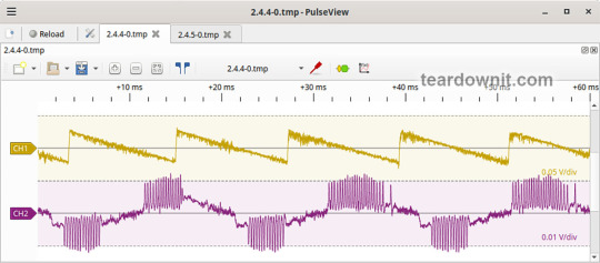
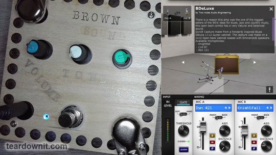
Brown Sound in a Box
He invented the superstrat, an electric guitar for shredding, a masterful style he pioneered. Of course, it's Eddie Van Halen, one of the world's greatest guitarists. Brown Sound is his signature sound, and we will try to recreate it today.
It all started in California in the first half of the twentieth century. Jazz developed rapidly. The musicians hunted for increasingly complex chords and incredible improvisations.
The usual banjo and mandolin no longer satisfied performing needs, and more and more jazz musicians became interested in the Spanish guitar. It has as many as six strings, at least 19 frets, and quart tuning, setting the mood for serious performance.
But the guitar turned out to be too quiet compared to wind instruments and pianos. Therefore, luthiers began to assemble jazzboxes with a body width of 16 to 19 inches—real mammoths! Pictured is an 18-inch Gibson Super 400.

Jazzboxes had an arched top body, similar to a cello, with f-holes instead of the traditional round ones for guitars. Jazzmen installed thick strings on them, 12 or even 13-gauge. The standard scale length was 25.5 inches, like the future Fender Stratocaster.
In 1921, Gibson began installing truss rods in the necks to withstand such high tension on steel strings. Among other things, this made it possible to create a low string height above the frets and subsequently create thin, fast necks.
Thanks to the truss rod, electric guitar virtuosos were able to improve. Especially since Gibson began producing instruments with a shorter scale of 24 ¾ inches, which is easier to bend. Then, guitars received an electromagnetic pickup and a tube amplifier, and guitarists wanted their sound to be even more loud and overloaded.
The hollow guitar body, critical in the pre-amplification era, became a nuisance: it was susceptible to microphone proximity effects and self-oscillation.
The hollow body also nearly killed sustain, as its essence was to transmit the strings' vibrational energy to the air. As a result, the sound is louder and brighter, but at the same time, it fades faster.

The first experiment in creating an electric guitar without a resonator body involved a lap steel guitar played with a slide. Finally, in 1950, Leo Fender created the Broadcaster, the first true, commercially successful solid-body electric guitar, which soon evolved into our beloved Telecaster.
While Gibson always created guitars as art pieces, Fender instruments were originally conceived as DIY kits. When the frets wear out, you can simply buy a new neck and replace it by removing four screws. There is no need to take your guitar to a luthier and wait for the repair, having no instrument on hand and thus being left with no income if you are a professional musician.
It is worth noting that the Broadcaster's neck had a serious technical flaw—the absence of an anchor. The Telecaster has this drawback eliminated. Vintage Fender guitars require removing the neck to tighten or loosen the truss rod. In contrast, more modern guitars have an Allen key screw in the base of the headstock to adjust the truss rod.
In general, Leo Fender's guitar parts were designed to be removable and attached with screws. This meant that the instrument could be purchased as a modular kit. One can put a humbucker instead of a single-coil and a Floyd Rose instead of a Fender tremolo machine with six self-tappers.

This is exactly what Eddie Van Halen did when creating his Frankenstrat. After all, he was a talented musician, artist, and craftsman. And he came up with the first superstrat in history, a guitar for the ultimate rock and metal.
The Superstrat badly needed super distortion, and we're not talking about the DiMarzio pickup with the same name. Eddie Van Halen's secret "brown sound" resulted from a rather complex sequence of electronic audio signal conversions, which is no longer a secret today.
Happy concertgoers and inspired TV viewers who followed Eddie's every move with bated breath saw a full stack of Marshalls with a Plexi head amp behind him. It was an excellent device, but many people had it.
Van Halen's secret recipe consisted of several ingredients. First, an MXR equalizer was hooked between the guitar and the amp input. It allowed Eddie to fine-tune the gain structure so that some frequency bands were boosted to hard clipping while others passed through the amp relatively unaffected.
Secondly, Variac's variable transformer connected the amplifier to a 120-volt electrical grid. It was powered by a voltage of 90 volts, 75 percent of the required. The tube cathodes were cooler, and the anode voltage was lower than during regular operation of the amplifier. This had a dramatic effect on the nature of the overload.
Thirdly, it was not the cabinets connected to the amplifier's output but the dummy load. This was not a modern reactive electronic load like the Torpedo Captor X, which simulates the impedance of real speakers. It was just a powerful tapped resistor providing the audio with the required amplitude.
Next, the signal went to the pedalboard with the flanger, phaser, and tape delay. From there, it goes to the MOSFET power amplifier H&H V800 and only then to the cabinets. Let's say Eddie implemented an effects loop, which his Marshall Plexi did not have.
Fourth, the cabinets were loaded with a specific combination of different speakers, which Eddie changed from time to time.

Van Halen subsequently moved on to use the Soldano SLO 100. Then he developed his signature 5150 amp with Peavey and the guitar Wolfgang, named after his son. Later, in collaboration with Fender, he created the EVH brand.

I had the EVH 5150 III lunchbox, which is just a great amp. Interestingly enough, the best room sound came not from the Celestion Greenback speaker but from the nameless black 12-inch speaker from the first-generation Fender Mustang II digital combo amp. I got the body and the speaker from this amp without electronics, and they became my favorite closed-back cabinet.

I also had a toy-like EVH 5150 III microstack. If we could add an output jack to an external cabinet, we'd feel some Van Halen vibes, but I didn't like the sound itself.
Unlike the Orange Crush Mini, this EVH product is more of a gimmick than a guitar amp. However, once I came across a YouTube video where this microstack sounded pretty good in an empty concrete room. Which once again proves the impact of the environment on the sound of an electric guitar.
As you can already tell, I like Eddie Van Halen's guitar tone. I don’t so much strive to recreate it as I look for inspiration. That's why building today's pedal is especially interesting for me.
In this diagram, we do not see the usual operational amplifiers. Instead, five JFETs are used here: four in two mu stages and one in a conventional common-source stage. The sixth JFET is responsible for the Millennium bypass. It simply turns off the LED when the gate of the transistor is connected to the ground through the volume control and lights the LED up when it's not.
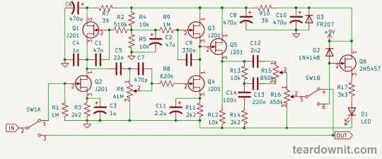
A mu stage is a cascade with an active load. In a simplified way, transistors Q1 and Q3 operation can be represented as current stabilizers. After all, a JFET is a current stabilizer controlled by gate voltage.
Resistors R4 and R5 form a virtual ground—a voltage source equal to half the supply voltage. It is AC grounded by capacitor C2.
We also see power filters. The C8R10C10 U-filter filters the power supply for the entire pedal, and the R7C6—for the first mu stage.
The active load transistor gates Q1 and Q3 are connected to virtual ground through resistors with significant resistances (R2 and R9). Capacitors C1 and C9 are connected between the sources and gates. Therefore, our active loads are not just current stabilizers but also active filters.
R6 is a gain control, and C7 is a treble bypass capacitor. The peculiarities of human hearing are such that when the volume is reduced, the sound seems duller, which is why the volume and gain controls are equipped with such frequency compensation in many devices.
Q5 serves as the output buffer, and R15 is the tone control. In the up position, the pedal outputs more high frequencies, and in the lower position, more low ones.
This is what this distortion sounds like with a Squier Bullet Mustang HH guitar and an Orange Micro Terror amp. I hear hints of the EVH sound in it. Still, it's more reminiscent of the Soldano SLO100 (which Eddie also used until the 5150 was developed).
Despite my stages and good power filters, the distortion is hairy. It must be put in a shielded housing for it to work typically. But even then, this circuit retains a fairly significant noise level.
However, these imperfections do not spoil the sound but make it more alive. If you want no noise, then an EVH 5150 amp is waiting for you to buy it. Fender engineers put a lot of effort into shielding and routing the boards of these high-gain amplifiers so that they are almost completely noise-free.
0 notes
Text
Methods of Implementing DC PLC Protocols
DC PLC communication mainly controls and monitors the condition of solar panels and energy storage systems. Additionally, DC PLC technologies are applied in industrial settings to supply power to electric motors and control them using a single pair of wires. All these applications suggest that the units responsible for communication over the power line are typically integrated into the corresponding devices (solar panel controllers, machines, and robots). Therefore, many automation system developers must understand how PLC protocols over DC power lines are implemented.
G3-PLC
The G3-PLC protocol is maintained by the international organization G3-Alliance.
Chipsets for this protocol generally comprise two microchips: an analog device for interfacing with the transmission line and a specialized microcontroller (SoC). In addition to signal processing, the microcontroller also handles encryption of the data transmitted over the line. The chipset may include a third chip responsible for converting the G3-PLC signal to one of the wireless protocols and back. Typically, this is the G3-Hybrid protocol designed for wireless networks to work alongside PLC. This protocol uses the 868 and 915 MHz frequency bands (which are not allowed for use in all countries).
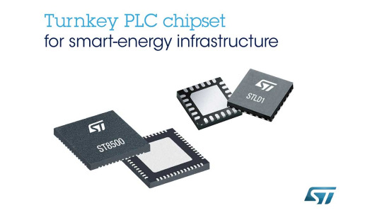
This is an example of a G3-PLC chipset from STMicroelectronics: on the left is the microcontroller, and on the right is the analog interface chip.
The chipsets and their firmware must be certified by the G3-Alliance to bear the G3-PLC label. However, such certification does not negate the need to certify G3-PLC solutions with national communications authorities if required by local regulations.
At least three manufacturers of G3-PLC chipsets are known: Maxim Integrated (a division of the US-based Analog Devices), STMicroelectronics (a European company headquartered in the Netherlands), and Vertexcom Technologies (China).
PLC-Lite
The implementation of this protocol is governed by TI's internal documents. The TMS320F28035 universal signal processor is used for signal processing. In addition, the receiver and transmitter must include the AFE031 line interface chip. The chipset also includes execution devices LM34910 and TPS62170.
IEEE 2847-2021
At the time of writing, a South Korean startup was producing devices supporting IEEE 2847-2021 (HPDS-PLC); the protocol is used in an LED lighting controller and a servo drive. Information about the components used for their development is not publicly available.
Data Transmission from Vehicle Batteries Sensors
A new technology that optimizes electric vehicle charging based on the battery's parameters and its wear level. Wireless sensors are installed on the battery. The wires inside the vehicle through which the charging current flows act as antennas. The signal passes through the electric vehicle charging connector. It continues to propagate along the charging cable as a guided medium. This solves the problem caused by the inability of radio waves to pass through the vehicle's metal body. A transceiver is connected to the cable at the charging station.
This solution uses one of the wireless protocols from the IEEE 802.15.4 family. The most widespread and cost-effective in this family is the Zigbee protocol. Therefore, it makes sense to use a chipset specifically for this protocol. Zigbee uses the 2.4 GHz band, and the frequency data transmission occurs along the charging station's cable. It should be noted that this solution is only possible for DC charging because, in this mode, the wires from the charging connector go directly to the battery.
Is software implementation of PLC algorithms possible?
For G3-PLC, using a general-purpose processor instead of a specialized microcontroller would require more chips than just two. Large production volumes and significant market competition produce relatively low prices for G3-PLC chipsets. These chips are manufactured across different regions—America, Europe, and Asia—ensuring a diversified supply. Therefore, developing a custom G3-PLC solution using general-purpose chips is not economically viable.
In PLC-Lite, a different company's signal processor can be used instead of TI's. However, new firmware would need to be written for it, which is quite costly. The TMS320F28035 is well protected from reverse engineering, so third parties cannot read the firmware stored in its memory.
No specialized chips are being produced yet for the IEEE 2847-2021 protocol, so its signal-processing algorithms must be implemented through the software on general-purpose microcontrollers.
It is more cost-effective to use specialized chips for creating PLC solutions.
The Zigbee protocol is implemented with a single chip that includes a microcontroller and a transceiver operating in the 2.4 GHz band. Using a general-purpose microcontroller would require a separate radio module, and interfacing these two units would be a highly complex task.
In conclusion, specialized chipsets are more cost-effective for PLC systems (except those using the IEEE 2847-2021 protocol).
0 notes
Text
Old School Digital Frequency Counter
Frequency in physics refers to the number of oscillation periods per unit time. To measure the frequency of electrical vibrations digitally, one needs to convert the waveform into pulses and count how many of those pulses have arrived over a certain time.
The simplest way to obtain pulses from different waveforms is to use a half-wave rectifier on diode D1, followed by a parametric voltage regulator on Zener diode D2, and a resistor R1.

The Zener diode limits the signal voltage not to damage the logic chips but to keep them operational. Resistor R1 limits the operating current of the Zener diode. Resistor R2 pulls the node output to the ground to protect it from interference.
Let's recall the diagram of an electronic clock from the other post. An electronic clock is a digital pulse counter. In this case, each digit is processed by a binary decimal counter on half of the CD4158 chip, decoded by the CD4511 decoder, and displayed on a seven-segment indicator.

Shift to the next digit is also done here, accounting for the specifics of each digit: seconds and minutes are counted up to 59, and hours—up to 23.
Counting hours, minutes, and seconds is a special case because we're used to it. Supposing we need a plain pulse counter where each digit works as a standard, In that case, it goes to zero and sends a carry pulse after nine—then a much more compact solution is possible.
In an electronic clock, for every two digits, we needed three and a quarter chips: two seven-segment decoders, one dual counter, and one 2AND logic element. The CD4081 chip has four of those.
And here, for a total of three digits, two chips are enough: a counter and a decoder! Moreover, four chips and three transistors allow us to count from 000000 to 999999!

This is the primary default circuit from the datasheet for the MC4553B, a 3-digit BCD counter. We will use it today in our frequency meter. But first, let's take a closer look at the operation of this fantastic chip.

It all starts with the pulse shaper and the DISABLE input, which, as the name suggests, disables counting if the voltage level is high.
Next, we have three BCD counters, precisely the same as the CD4518 halves we've used in the digital clock.
3ANDs are used for carrying (and that's just what they do); if Q0 and Q3 are ones, that is, we have the number b1001 = 9, and the next clock pulse arrives, then a carry pulse is generated, and the counter goes to b0000 = 0.
When the chip counts to 999, and the next pulse arrives, it goes to 000 and sends a carry pulse to the OVERFLOW output.
The diagram below shows the MR (Master Reset) input. When a logical one arrives at it, all four counters are reset, as well as the scanner, which we will cover a little later.
Next, we see three 4-bit latch registers. We discussed a shift register with a latch function thoroughly in the post. To be brief, the register is 'transparent'. It simply transmits data from the inputs to the outputs as long as the input LE (LATCH ENABLE) is low.
A logical one at LE makes the register stop responding to the state of the inputs, saving the stored states at the outputs.
This is an excellent feature for meters with indicators because it allows the readings to be frozen so that a person can actually read them.
Flip-flops are also used, for example, in analog-to-digital conversion, to preserve the finished, complete result and not confuse it with the intermediate one. Latches are also a necessity for data communication modules.
If you program microcontrollers, then you probably know that their peripheral architecture contains many latched registers, and the code often interacts with them.
This is very convenient, allowing asynchronous peripherals to work independently without adding processing load and wasting program memory. And if and when an interrupt or a flag state indicates the presence of a ready result, the program can start processing it.
Data from the outputs of three four-bit latching registers is supplied to a multiplexer controlled by the scanner.
This scanner is a counter-decoder, similar to our trusty CD4017. Only the CD4017 counts from 0 to 9, and the scanner counts from 0 to 2 or 1 to 3, whichever you prefer best.
The scanner is clocked by an oscillator, and the oscillation frequency is set by capacitor C1. And if this capacitor is absent, then clocking can be done from an external source.
So, at the outputs Q0..Q3, we will have a binary representation of a digit, and the number of this digit, the register, is output to the ¬DS1..¬DS3. We'll have a low level at a single output, corresponding to the position of the output digit.
With the help of a multiplexer and a scanner, we can get by with just one seven-segment decoder for three bits! We use MC14543B here, and it works exactly like the CD4511 in the clock application.
This economical way of displaying the digits, when they are shown one after another, is called dynamic and is very often used in projects with microcontrollers.
In this diagram, we see that all six indicators are activated by three transistors from the left MC14553B chip. The scanner on the correct chip is synced with clock pulses from the left one.
And for each of the three-digit decimal counters to start outputting readings from the same first digit, the MR input (MASTER RESET) resets the scanner and the counting registers.
So, we connected our two-diode pulse shaper to the CLOCK INPUT and got ourselves a pulse counter from 0 to 999999.
To turn this counter into a frequency meter, we need to program the following sequence:
Perform a master reset of both counters.
Allow the counters to count pulses for one second.
Latch the indicators for three and a half seconds so they can be read.
Go to step 1.
Do we need a microcontroller, then? Not really; a sequencer can handle such a simple task.
Here, we have a quartz-stabilized clock generator that produces a frequency of 2 hertz, precisely the same as in our homemade clock. And the role of the sequencer is played by our beloved CD4017; it just needs some help from eight diodes.
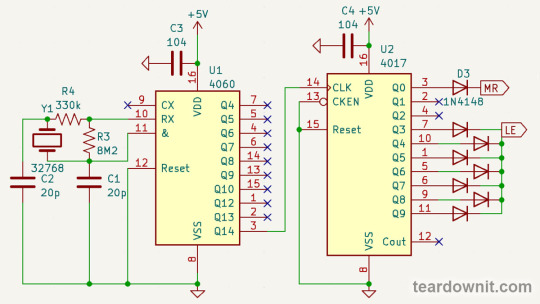
When output Q0 is high, our pulse counter gets a master reset. Then, a second passes until the logical one moves to Q1 and then to Q2. It is not output anywhere; the counter continues to count for itself.
As soon as a second has passed, the counter has registered the number of pulses corresponding to the input signal frequency. Then, the logical one from Q3 sends the LATCH ENABLE signal.
The pulse counter continues to count, but this does not affect the indicator readings, and they stay put for three and a half seconds.
Then, the logical one is once again at Q0, a master reset occurs, and the cycle repeats.
This is how our DIY frequency meter works, which we've managed to program using just diodes and no microcontroller.
0 notes
Text
Review, teardown, and testing of ERPF-400-24 Mean Well power supply
General Description

Brief Specification: ERPF-400-24 is a power supply unit with a 24-volt DC output and a rated current of up to 16.7 amps. According to the specification, the unit has an extended operating range for AC input voltage from 90 to 264 V. However, with an input voltage between 90 and 200 V, the unit can only deliver 50% of its rated power. It can also operate from a DC input within the range of 127 to 370 V.

The unit has dimensions of around 9x5x2 inches (220x130x48 mm exactly), is built on a printed circuit board housed in a stamped metal case, and is designed to operate with no forced cooling. The board is installed into the case, like in a tray, and is covered with a compound (most likely thermally conductive), making it non-removable for repair. The unit is covered with a perforated lid on top.
It features an LED indicator for output voltage and allows adjustment of the output voltage within a range of -5% to +10%. The unit includes an active PFC (Power Factor Correction) circuit and has a high power factor of up to 0.98 at 115 VAC. It also has thermal protection, with temperature monitoring performed using a thermistor placed on the output rectifier diodes. Traditional safe measures, such as overload and overvoltage protection, are also provided.
Circuit and construction description: Unfortunately, the compound filling makes detailed examination of the circuit difficult, so there is a high probability of interpretation errors. However, it appears that the design shares many similarities with the RSP-320-24 (https://teardownit.com/posts/review-teardown-and-testing-of-rsp-320-24-mean-well-power-supply) power supply unit, in both circuit and layout. This suggests that the ERPF-400 may be controlled by the FAN4800 controller, just like the RSP-320.
The input and output terminals are mounted on a common screw terminal block (1). The terminal block's connections from top to bottom are as follows: three terminals for phase, neutral, and ground (input), and three parallel terminals for the output, ground, and +24V. The input voltage from the terminal block (1) passes through an EMI filter (3) and then to the diode bridge (5). A varistor (2) is installed at the filter's input to suppress dangerous voltage spikes. The rectified voltage from the bridge (5) is then routed through an NTC inrush current limiter (4) to the active PFC circuit. The PFC's power stage consists of a transistor (6), inductor (11), diode (7), and output capacitor (8). The rectified and filtered voltage from capacitor (8) is fed into a forward converter, which comprises transistors (9) and transformer (10). The voltage from the transformer's output winding (10) is rectified by diodes (12) and filtered by an output LC filter (13) (14).
The filter’s output capacitance is provided by four 560µF, 35V capacitors rated for operation at up to 220°F or 105°C (13).
The transformer's core (10) is tied in a metal clamp, which is bolted to the case. This design likely serves to dissipate heat from the transformer.
Due to the presence of the compound, it is difficult to assess the overall build quality. The compound itself has been applied somewhat carelessly, with visible splatters and drips. Furthermore, there are gaps in the compound application, significantly reducing its protective effectiveness.


The LED output voltage indicator and output voltage adjustment resistor (16) are located near the terminal block, allowing access without removing the top cover.
Test Conditions
Most tests were conducted using Test Circuit 1 (see appendix) at 80°F (27°C), 70% humidity, and 29.8 inHg pressure. Unless otherwise specified, measurements were taken without pre-warming the power supply, and the operating mode was momentary load. Input voltage was set to 115V AC, and the current of 8.4 A was considered 100%. The following values were used to determine load levels:

Output voltage with static load

The unit demonstrates excellent output voltage stability.
Startup Characteristics
Startup at 100% load
Before the test, the power supply was turned off for at least 5 minutes with the load connected at 100%. The startup waveform at 100% load is shown below (Channel 1: output voltage, Channel 2: input current):

The startup process can be divided into three phases: 1. Input current pulses charging the input capacitors upon connection to the grid, with a peak amplitude of about 3 A, consisting of two portions of one period each. 2. Waiting for the control circuit to start, about 231 ms. 3. (Output Voltage Rise Time) Output voltage rise, 57 ms. 4. (Turn On Delay Time) The total time to reach operational mode from power-on is 288 ms.
(Output Voltage Overshoot) The startup process is aperiodic with no overshoot.
Startup at 0% load
Before the test, the power supply was turned off for at least 5 minutes with the load connected at 100%, then the load was disconnected, and the unit was turned on. The startup waveform at 0% load is shown below:
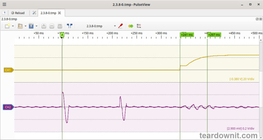
The startup process consists of three phases: 1. Input capacitors charging upon connection to the grid, with a peak amplitude of about 2.6 A, consisting of two portions of one period each. 2. Waiting for the control circuit to start, about 241 ms. 3. (Output Voltage Rise Time) Converter startup, output voltage rise, and transition to operational mode, 56 ms. (Turn On Delay Time) The total time to reach operational mode from power-on is 297 ms.
(Output Voltage Overshoot) The startup process is aperiodic with no overshoot.
Shutdown Characteristics
The shutdown process was tested at 100% load with nominal input voltage at the moment of shutdown. The shutdown waveform is shown below:

The shutdown process can be divided into two phases: 1. (Shut Down Hold Up Time) The unit continues operating, powered by the charge stored in the input capacitors, until their voltage drops to a critical level at which maintaining the output voltage is no longer possible. This phase lasts for 26 ms. 2. (Output Voltage Fall Time) Output voltage decline, converter stop, and acceleration of the voltage drop. This phase lasts for 25 ms.
(Output Voltage Undershoot) The shutdown process is aperiodic, with no undershoot.
Current amplitude at 100% load prior to shutdown was 2.8 A.
Output voltage ripple
At 100% load:
low-frequency ripple of about 10-12 mVp-p at twice the grid frequency, and around 4 kHz with a ripple of 13-15 mVp-p.

At the converter frequency, ripple is approximately 25 mVp-p, with noise at 120 mVp-p.

At 75% load:
low-frequency ripple of about 10 mVp-p at twice the grid frequency and around 12 mVp-p at approximately 4 kHz.

Converter frequency ripple is about 20 mVp-p, with noise at 100 mVp-p.

At 50% load:
low-frequency ripple of about 10 mVp-p at twice the grid frequency and around 15 mVp-p at approximately 4 kHz.

Converter frequency ripple is about 20 mVp-p, with noise at 100 mVp-p.

At 10% load:
low-frequency ripple of about 3-5 mVp-p.

Converter frequency ripple is about 20 mVp-p, with noise at 100 mVp-p.

At 0% load:
The input current was measured with a multimeter at 60 mA. (Power Consumption) Input current in this mode is primarily reactive in nature; thus, the power consumption value measured with handy instruments can't be correct. The input filter has two capacitors, according to the diagram.
At 0% load, low-frequency ripple is hardly distinguishable from the noise, about 3 mVp-p.

Converter frequency ripple is masked by noise around 100 mVp-p.

Dynamic characteristics
Dynamic characteristics were assessed in a mode that switches between 50% and 100% load. The oscillogram below illustrates the process:

It is evident that the unit's response to step-load changes is aperiodic, with the magnitude of the response to load changes being approximately 100 mV p-p.
Overload protection
The manufacturer specifies overload protection with a constant current limiting type, which was confirmed during testing. When overloaded or the output terminals are shorted, the unit enters current limiting mode and automatically recovers after the fault is removed.
The output current at which the limit is triggered is 22 A.
Input safety assessment
(Input Discharge) The input circuit discharge time constant was measured upon disconnection from the grid, with a value of 0.245 s. This means that when operating on a 120V grid, the time required for the input circuits to discharge to safe levels (<42 V) is 0.39 s:

Important: This result applies only to the tested unit and was obtained exclusively for research purposes. It cannot, under any circumstances, be considered a guarantee of safety.

The ground leakage current was measured at 73µA.
Thermal behavior
No significant heating of components was observed during no-load operation. Thermograms were taken at three power levels—80%, 90%, and 100%—with and without the top cover. The thermograms show that the most thermally loaded components of the unit are the NTC inrush current limiters (4), which stand out from the other components. At 80% load, the NTC temperature is 175.6°F (80°C, with a 53°C rise above ambient temperature); at 90% load, it reaches 192.1°F (89°C, with a 62°C rise); and at 100% load, it reaches 203.9°F (95.5°C, with a 68.5°C rise).
The second hottest component, after the NTC, is a resistor, 25 degrees cooler.
80% load
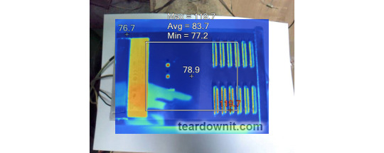

90% load


100% load


Conclusions
The ERPF-400-24 generally exhibits low noise and ripple, and it maintains good accuracy in sustaining the output voltage. The unit has decent dynamic characteristics, responding to pulsating loads without overshoot.
On the startup waveform (see oscillograms), there is an N-shaped section where, after the initial rise in output voltage, a partial drop occurs, followed by another rise and stabilization at the nominal level. This behavior could potentially cause issues when powering up digital devices that require initialization.
The build quality is good. However, the compound is applied somewhat poorly, with notable imperfections and several gaps. Unfortunately, these gaps affect components with increased hygroscopicity, particularly the wire-wound inductances of the output and input noise filters. Despite the manufacturer's claim of “protecting the internal electronic components from rain splash and dust,” this unit should not be used without additional water ingress protection.
According to the specifications, the unit is designed for operation under conditions of "Cooling by free air convection" and "-22F ~ +140°C (Refer to output load derating curve)." The tested unit indeed remains safe up to 100% load during continuous operation. The presence of a temperature sensor on the rectifier diodes adds extra assurance of safety.
Important: The results and conclusions presented apply only to the tested unit and were obtained solely for research purposes. Under no circumstances should they be used to assess all devices of this type.
0 notes
Text
Telecommunication protocols application interaction
Let's look at the basics of transferring information between two application processes in the OSI model.
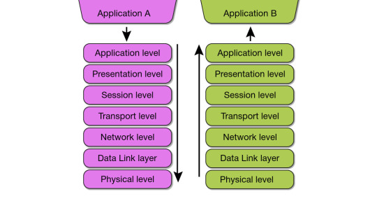
Say an application (in the picture above) needs to access a file service on another computer. It sends a request to the application layer. Based on it, the software generates a standard format message consisting of a data field and a service header. The latter contains a description of actions for the application layer of the other machine to perform, as well as instructions for the adjacent lower layer. The presentation layer, in turn, formats the data according to the instructions received and adds its own header (some protocol implementations also include service data at the end of the message), after which the information is sent to the session layer. This procedure, called encapsulation, is repeated further as data and service information move to the physical layer.
When arriving at the physical layer, i.e., the network, data passes through many other devices (network adapters, hubs, routers, bridges, etc.) and, upon reaching the destination (for example, a SIP phone), undergoes a reverse encapsulation process (right side of the picture).
Data networks can be of two types: local (local area network, LAN) and global (wide area network, WAN). The latter connects any two networks within the globe with dedicated or switched communication channels. Local networks differ in transmission medium, topology, and access control. Depending on the transmission medium, they are divided into wired (using coaxial, twisted pair, or fiber-optic cable) and wireless (WLAN), and according to the type of topology, into networks with 'bus', 'ring', or 'star' topologies.
Each computer on the local network is connected to the transmission medium through a special adapter that "sees" what any other adapter on the same network is transmitting; such systems are called broadcasts.
The MAC protocol regulates the sequence of nodes' access to the transmission medium. It is implemented using two types of schemes: polling or contention-based MAC schemes.
MAC polling networks can be centralized or distributed. Centralized ones have a star topology with a hub as the control node. In contrast, distributed ones have a ring or bus topology with token passing. Contention-based MACs are often implemented as carrier sense multiple access with collision detection (CSMA/CD) or carrier sense multiple access with collision avoidance (CSMA/CA). The first is used in all types of Ethernet LANs, and the second is used in most wireless WLANs.
The unrivaled leader among local networks is the IEEE 802.3 Ethernet network, where coaxial, twisted pair (designated by the letter T for 'twisted') and fiber-optic cables are used as transmission media. The transition to twisted-pair cable made it possible to implement full-duplex transmission over two twisted pairs, leaving the concept of collision meaningless since transmission and reception became independent operations. Ethernet has transmission speeds of 10, 100 ('Fast Ethernet'), 1000 Mbit/s (1 Gbit/s, 'Gigabit Ethernet'), and up to 400 Gigabit Ethernet.
Wireless local networks (wireless LAN, WLAN) have also become widespread. Their parameters are stated in the IEEE 802.11 specifications, known as Wi-Fi.
Today, the most common Wi-Fi 5 or 802.11ac defines the operation of wireless local area networks in the 2.4/5 GHz ranges with a data transfer rate of 1.3 Gbit/s. Shortly, speeds will reach 9.6 Gbit/s over 6 GHz frequency bands.
The range of most WLAN systems is 120 m, depending on the number and type of obstacles encountered. Additional access points will help expand the coverage area. Using two or three carrier frequencies instead of one can increase the number of users and network capacity.
Obviously, with Wi-Fi, network security becomes an important issue. A priori, wireless networks must be equipped with additional means of ensuring reliability compared to wired ones. WLAN uses direct sequence spread spectrum (DSSS) technology, which is highly resistant to data corruption and interference, including intentional ones. The problem of user authentication can be solved by introducing system identifiers. The wired equivalent privacy (WEP) mode is provided to transmit necessary information. In this case, the signal is encrypted with an additional algorithm, and the data is controlled using an electronic key.
Like all IEEE 802.3 standards, 802.11 refers to the lower two layers of the OSI model: physical and link. Any network application, operating system, or protocol (such as TCP/IP) will function equally well on an 802.11 network or Ethernet one.
The original 802.11 standard defines the basic architecture - the features of 802.11 services. The 802.11x specification only addresses the physical layer, introducing higher access speeds.
In conclusion, we should note that thanks to the close ties between Ethernet and the IP protocol, the scope of Ethernet applications is expanding, particularly in broadband subscriber access (BSA) networks.
0 notes
Text
Why there are so many diverse Tube Screamers?

Recently, I realized that I had never built a Tube Screamer before. This gap must be filled. It also makes sense to figure out which Tube Screamer I need and which is better for you. After all, if you play an electric guitar, then you probably need it in your life!
The Tube Screamer is probably the most popular of all guitar pedals. Especially if you count in numerous clones, mods, and pedals built based on the Tube Screamer circuit.
The scheme has proven to be so fitting that it suits most styles of guitar music, from light rock and blues to the heaviest styles with eight-string, low-tuned guitars.
The Tube Screamer has a nice-sounding overdrive of its own, ready for the clean channel of a pedal platform. It can also help to overdrive a vintage amp.
Or it can make the sound of a modern high-gain amplifier more focused by emphasizing the desired frequencies and preventing the amplifier from choking and squealing due to an excess of unwanted frequencies. And ensure the notes are legible while maintaining the warmth of the solo.
The legendary green pedal with a rectangular button and the number 808 in the name entered the market in 1979. Its name did not contain the phrase "Tube Screamer." It was produced not by Ibanez but by another Japanese company, Maxon. It continued to make the OD-808 and OD-9 for Ibanez and under its own brand.

Maxon employee Susumu Tamura not only developed the circuit and case for the Overdrive OD808 but also came up with the name Tube Screamer Overdrive Pro, which is already for the Ibanez TS808.

Today, early examples of the Maxon OD808 and Ibanez TS808 are highly collectible. This screenshot from Reverb shows the prices that are considered not that high. However, there's always a chance to find it in a pawn shop or local market.
Like most guitar pedals and amps, the Tube Screamer's circuit was not designed from scratch. Enthusiasts of guitar electronics and analog synthesis love to disassemble the products of their colleagues and improve or rearrange something in them to create unique devices based on what they have learned.
In 1977, the Roland BOSS Corporation, also from Japan, released the OD-1 overdrive pedal. Let's look at its diagram, starting from the power stage in the lower left corner.

The power socket is connected through diode D4 and resistor R15. Together with capacitors C11 and C8, R15 forms a U-shaped power filter.
Why is diode D4 needed? To protect against reverse polarity, the circuit has a Zener diode D5. It also protects the pedal from overvoltage above 11 volts. Diode D4 does not act as a rectifier either since the pedal is designed to be powered by a DC adapter.
In the post about the legendary BOSS DS-1 distortion, we've already seen precisely this power supply circuit. And we have found out that this is not just a filter or additional protection but also an analog simulation of the voltage drop of a 9-volt molten-salt battery. This stage is found in many early BOSS pedals, improving the tone.
We will not show the bypass JFET circuit since we discussed it in the same article. It's precisely the same, and many enthusiasts don't like it, preferring true bypass instead.
True bypass with LED indication can be implemented using a 3PDT foot switch. You can get by with DPDT if you use the Millennium bypass indicator circuit described in the post on Brown Sound in a box.
The virtual ground, indicated in the diagram by a diamond, is formed by resistors R7 and R8. They have equal resistance values and divide the supply voltage in half. Capacitor C3 grounds the virtual ground for alternating current.
The input and output buffers on transistors Q1 and Q2 are the usual emitter followers.
An overdrive section is built on the operational amplifier U1A, and an active filter is made on U1B. Most of the first BOSS OD-1 pedals used Raytheon's RC3403ADB quad op-amps.
But sometimes, you can find a copy with the uPC4741C chip from the Japanese company NEC. This is neither a counterfeit item nor a refurbished pedal, but a genuinely original BOSS OD-1. Known examples with uPC4741C were produced in 1978.
Roland/BOSS then stopped using the quad op-amp as a dual op-amp, and later pedals contained the 4558 IC with different indexes.
What does the 1977 BOSS OD-1 have to do with it when we're talking about the 1979 Maxon OD808, you might ask? Just have a look at the OD808 diagram.

As you can see, these two schemes have a lot in common! Several components have been swapped for different values compared to the BOSS OD-1. Capacitors C5 and C6 have been added; C9 has been removed.
The D3 diode was also excluded, so clipping became symmetrical instead of asymmetrical. And most importantly, the R14 tone control has been added. It started as a pedal with two knobs; now it has three.
This time, BOSS studied Maxon's overdrive and, in 1981, released the SD-1 Super Overdrive! Here is its diagram.

Some call this practice stealing ideas, but BOSS, Maxon, and Ibanez ultimately benefited from it, as did the guitarists and listeners. The more different pedals with different nuances, the better!
Next came the TS9 and many other Tube Screamers and overdrives from various manufacturers. My pick is the MXR ZW44 circuit.

This is a Zakk Wylde signature pedal; at its core, it is still the same Tube Screamer. Or rather, SD-1 Super Overdrive because the limitation here is asymmetrical.
I enjoy the range of tone, gain adjustments, and how Tube Screamer's volume control affects the amp's overdrive. You can get a lot of different sounds and fine-tune their shades.
Without Tube Screamer, the amp responds to the gain knob input differently because it is the overdrive pedal that determines the frequency bands that will be emphasized. And this is the primary purpose of the pedal.
0 notes
Text
Communication protocols for PLC on DC lines
The main feature of any PLC system, whether on DC or AC lines, is that communication uses cables initially designed for power delivery. This results in the following challenges:
Cable parameters are not certified for the PLC system frequencies
No impedance matching between line elements, leading to multiple signal reflections
No protection from external interference
No shielding from radio waves emitted by the line
Interference caused by load switching and, for DC lines, DC-DC conversions
The signal transmitted via the power line can be intercepted into the surrounding space
The following solutions are known to address these issues:
Limiting maximum transmission speed to tens of kbps is fine for control systems
Using modulation types that are resistant to reflections and interference
Selecting frequency ranges free from strong interference, such as the one from electronic ballasts of fluorescent lamps
Choosing frequency ranges where radio stations and critical broadcast systems do not operate
Using appropriate DSP algorithms to combat interference and reflections
Modulation
Previous generations of PLC systems used FSK (Frequency Shift Keying) modulation and its variants, where data is transmitted by abrupt frequency shifts. This modulation type inefficiently uses the spectrum, so data rates in PLC systems using FSK rarely exceed 2.4 kbps. Most modern PLC systems use OFDM (Orthogonal Frequency-Division Multiplexing), where information is transmitted on several orthogonal subcarriers at equal frequency intervals. Each subcarrier is modulated using quadrature amplitude modulation or amplitude-phase shift keying. OFDM's main advantage is its resistance to multiple reflections. Additionally, OFDM uses the frequency spectrum more efficiently, allowing higher data rates than FSK without expanding bandwidth.
PLC-G3
This protocol is used on both AC and DC lines. The maximum transmission speed for commercial equipment is up to 45 kbps (the theoretical limit is 234 kbps), with a communication range of up to 1300 feet. In Europe, it operates in the 35.9–90.6 kHz (GENELEC A) and 98.4–121.9 kHz (GENELEC B) bands; in the USA, it operates in 154.7–487.5 kHz (FCC), and in Asia, 154.7–403.1 kHz (ARIB). The advantages of PLC-G3 include its universality and international standardization (ITU-T G.9903), ensuring full equipment compatibility within a region of the same frequency. It is currently used to control green energy systems, collect data from electricity meters, and send consumption limitation signals to the equipment of non-paying customers. Data is encrypted with AES-128.
PLC-Lite
The PLC-Lite protocol is promoted by TI and designed for DC lines with voltages from 18 to 35V, typically 24V. PLC-Lite operates in the 42–90 kHz frequency range with data rates up to 21 kbps.

A PLC isolation scheme for DC lines by TI (https://www.ti.com/)
The main advantage of this protocol is its cost-effectiveness (today, a low-frequency 60 MHz processor is sufficient). TI also provides a ready-to-use set of chips and software, simplifying equipment production. The disadvantages include a communication range limited to 130 feet and dependency on a specific manufacturer, which reduces the selection of available proprietary components. This protocol is mainly used in factories with robots. It transmits both 24V power and control signals over the same cable. Since PLC-Lite systems are typically used within a single factory floor, encryption is not provided by default.
IEEE 2847-2021
This protocol supports data transmission over DC power lines at speeds up to 9.6 kbps. The line voltage must not exceed 50V, and the load power can range from 10 to 2000 watts, with a minimum power supply output of 100 watts. The communication range is up to 3300 feet. The protocol covers nearly all possible PLC use cases for control purposes, such as lighting, motors, energy storage, UPS systems, and solar power generation. The protocol is based on HPDS-PLC (High Power Differential Signal) technology, which uses differential transmission. Identical signals with a 180-degree phase shift are sent through two wires, and at the receiving end, one signal is subtracted from the other, doubling the transmitted signal. External interference affects both wires equally and is mainly canceled out. This also reduces electromagnetic interference emitted by the PLC system. As a result, the transmitted signal's power can be increased, enhancing resistance to interference from DC-DC converters. Although IEEE is based in the US, its standards are recognized worldwide. HPDS-PLC is expected to be well-standardized and has good equipment compatibility. The protocol offers the longest communication range among PLC protocols on DC lines. However, the data transmission rate is limited to 9.6 kbps, which is relatively minimal by modern standards, even for electrical equipment control. Additionally, some power line constraints, such as LED lighting, may be excessive. The standard is still very new (introduced in 2022), and no known widespread equipment has yet to support it.
Microwave Systems for Electric Vehicles
A new direction in DC PLC development is data exchange via a DC charging cable between smart EV battery sensors and the charging station. This allows the battery to charge optimally, considering its parameters and wear.

PLC systems enable data to be gathered from electric vehicle battery sensors via the charging cable
For this, data transmission occurs on freely available frequencies (868 MHz and 2.4 GHz), with the charging cable acting as a waveguide for radio waves. The radio signal cannot pass through the metal body of the electric vehicle. Still, it can travel inside and outside through the wires connected to the charging port. The internal wiring serves as an antenna, and sensors on the battery exchange data wirelessly. This technology still needs to be standardized, but it can utilize well-established solutions from wireless communication systems.
Conclusions
The main applications of DC PLC are in solar energy and industry. In both cases, long communication ranges (in AC power lines of 6–35 kV, the PLC signal can travel up to 6 miles) and high data rates are not required. More important is cost-effectiveness. If PLC equipment becomes too expensive, installing additional signal cables or wireless systems becomes more viable. Therefore, the communication protocol parameters are a reasonable compromise to achieve an acceptable price point.
0 notes
Text
A simple DIY guitar tremolo pedal
Have you ever thought of making your guitar sound differently or just livening things up a bit? In addition to reverb and chorus, a subtle tremolo can help. Today, I will build a very simple tremolo pedal using three transistors.

Of all the time-based effects, electronic tremolo is the easiest to get.
The important thing is that one does not need to alter amplifier bandwidth for tremolo, like in wah pedals and phasers, by electronically reconfiguring frequency-dependent circuits containing active and reactive resistances—resistors, coils, and capacitors.
There is no need to implement, much less modulate, the signal time delay. This is done in delays, reverbs, flangers, and choruses using mechanical, analog (bucket brigade devices, BBD), and digital delay lines.
Moreover, there is no need to process the frequency of the input signal. Raising the frequency by an octave is relatively simple; it takes a full-wave rectifier, similar to those used in power supply units.

A full-wave rectifier folds the wave. It turns the lower half-wave up, and now there is a whole period of the output signal for each half-cycle of the original signal.
We have doubled the fundamental frequency and added some harmonics. After all, the output signal is no longer sine. The upper half-wave is smooth, and the lower half-wave is pointy.
The first octave did not use a bridge rectifier with four diodes but a half-bridge rectifier with two diodes and a transformer with the winding having a midpoint.
Such a transformer was easy to find. For example, a phase-inverter matching transformer from a pocket transistor radio could do. We've put together a receiver of this kind in a post about the Regency TR-1.

It is unnecessary to use a transformer if you build a full-wave rectifier using operational amplifiers.

And finally, when making a phase inverter for a full-wave rectifier, you can do it without operational amplifiers. One transistor is enough. After all, the output signal at its emitter has the same polarity as the input signal at the base, and at the collector, it has inverted polarity.

Suppose the signal frequency needs to be decreased by half, not increased. In that case, that is, by one octave, then synchronous D-flip-flops, which we've discussed in previous articles, will be helpful.

A circuit divides the oscillator frequency on a 555 timer by 2, 4, 8, and 16. That is, by two to the first, second, third, and fourth powers. And if we speak musical terminology, we lower the tone by one, two, three, and four octaves.
However, electric guitar pickups do not produce digital pulses or even a sine wave but an analog signal of a complex shape with many harmonics. So, to divide the frequency with flip-flops, the guitar signal must be preprocessed by converting it into rectangular pulses.
One possible circuitry answer to this problem is in the diagram of this old Japanese pedal. Here, the signal on its way to the latches passes through a compressor and a Schmitt trigger.

The compressor is needed to process both loud and quiet notes effectively. Interestingly, the CMOS NAND gate circled in green on the diagram, is used as an analog signal amplifier.
This is doable. The ratio of the resistor value between the output and the inverting input of the CMOS inverter to the impedance in series with the input determines the gain, just like in an operational amplifier.
An excellent example of a pedal that uses CMOS inverters rather than transistors, op-amps, or tubes to amplify the guitar signal is the Tube Sound Fuzz circuit, designed by Craig Anderton and published in his 1975 book "Electronic Projects for Musicians."

Frequency dividers on flip-flops work well with a single note. And for a chord or pitch shifting at an interval of a non-integer octave number, a digital signal processor is almost always required.
Perhaps the only exception is the perfect fifth. The original frequency must be divided by three and multiplied by two to obtain it. Frequency division into three is possible using a single CD4013 chip containing two synchronous D-flip-flops with asynchronous setup and reset.

At each of the points of the circuit, marked with numbers 2, 3, and 4, there is a frequency from point 1, divided by 3, in the form of a PWM signal with a duty cycle of 2/3 or 1/3. For music, this sounds even better than a duty cycle of 1/2.
The phases of the signals at these points are shifted between each other, which can also be used for interesting sound effects. But there is one problem.
Modern music uses not natural but evenly tempered tuning. Therefore, our electronic fifth, played by flip-flops, will be slightly out of tune relative to the fifth on the guitar frets.
The frequency of this equal-tempered fifth is not equal to two-thirds the frequency of the original note but to the frequency of the original note divided by the 12th root of 128. This system allows one to freely transpose melodies and chord progressions from one key to another. That is why it became universally recognized.
And to get a tremolo, you don’t need all these tricks. Two functional blocks are enough: LFO and VCA, a low-frequency oscillator, and a voltage controller amplifier.
Each of them can be implemented literally on one transistor. This is precisely what the developers of the Univox/Unicord U65RN combo amplifier, produced since 1971, did.
Frequency dividers on flip-flops work well with a single note. And for a chord or pitch shifting at an interval of a non-integer octave number, a digital signal processor is almost always required.
Perhaps the only exception is the perfect fifth. The original frequency must be divided by three and multiplied by two to obtain it. Frequency division into three is possible using a single CD4013 chip containing two synchronous D-flip-flops with asynchronous setup and reset.
At each of the points of the circuit, marked with numbers 2, 3, and 4, there is a frequency from point 1, divided by 3, in the form of a PWM signal with a duty cycle of 2/3 or 1/3. For music, this sounds even better than a duty cycle of 1/2.
The phases of the signals at these points are shifted between each other, which can also be used for interesting sound effects. But there is one problem.
Modern music uses not natural but evenly tempered tuning. Therefore, our electronic fifth, played by flip-flops, will be slightly out of tune relative to the fifth on the guitar frets.
The frequency of this equal-tempered fifth is not equal to two-thirds the frequency of the original note but to the frequency of the original note divided by the 12th root of 128. This system allows one to freely transpose melodies and chord progressions from one key to another. That is why it became universally recognized.
And to get a tremolo, you don’t need all these tricks. Two functional blocks are enough: LFO and VCA, a low-frequency oscillator, and a voltage controller amplifier.
Each of them can be implemented literally on one transistor. This is precisely what the developers of the Univox/Unicord U65RN combo amplifier, produced since 1971, did.
It had 15 watts of power, a 12-inch loudspeaker, and a spring reverb. It was assembled according to a relatively simple circuit by today's standards. However, at that time, it was considered quite complex.

Our attention should be drawn to the lower left corner, which shows the tremolo diagram. The leftmost transistor is used in the phase-shifting RC LFO. This generator produces harmonic sine waves, the frequency of which is controlled by the SPEED potentiometer.
Oscillations from the LFO output go to the modulation intensity control INT and to the second transistor's base. This transistor simply bypasses all input signals from the microphone, guitar, and organ. This is how the VCA is made.
And the tremolo pedal jack simply shorts the LFO signal to the ground, and the VCA transistor is completely turned off. This allows one to turn the tremolo on and off using a pedal with just a latching SPST button inside.
The diagram published by Anthony Leo in the November 1968 issue of Electronic Australia Magazine, 3 years before the Univox/Unicord U65RN, differs slightly from the tremolo found in this combo amp.
Since then, the circuit has been called the Electronic Australia tremolo or EA tremolo for short. It's a beloved one among pedal enthusiasts.

Here, the VCA comprises a common-emitter bipolar transistor Q1 and a JFET Q2 that bypasses most of Q1's AC bias resistance, thereby modulating the stage's gain.
I've assembled this DIY pedal kit from Landtone using just this scheme. In the video below, you can hear the resulting sound.
Due to such an exciting circuit design, the effect turned out to be very beautiful. This is the best tremolo I have ever encountered.
As we can see and hear with our own eyes and ears, excellent results can be achieved using simple means if you approach the project thoughtfully and with love.
0 notes