#10 layer PCB
Explore tagged Tumblr posts
Visit Tumblr Blog
Explore Tumblr blogs with no restrictions, modern design and the best experience.
Last Seen Tumblr Blogs


Fun Fact
The Tumblr office adopted Tommy, an 11-year-old Pomeranian.
Text

10 layers high density interconnect PCB board made of FR-4, Tg 150 with immersion gold surface treatment.
High-Density Interconnect (HDI) PCB is simply a PCB with more number of interconnections and buried hole, blind hole, occupying minimal space. This results in the miniaturization of the circuit board. The components are placed closer and the board space is significantly reduced but the functionality isn’t compromised. [email protected]
4 notes
·
View notes
Text
Benefits of Multi-Color PCBs in Circuit Design
Multi-color printed circuit boards (PCBs) are transforming the landscape of electronic design by blending functionality with aesthetics. One of the primary benefits of multi-color PCBs is that different colors can indicate specific circuit functions or components, helping engineers and technicians quickly identify issues during manufacturing and testing. , the use of multi-color PCBs can improve thermal management and signal integrity

#PCB manufacturer#PCB fabrication In india#custom PCB manufacturing in india#prototype PCB manufacturing#low-cost PCB manufacturer#high-quality PCB manufacturing#quick turn PCB fabrication#flex PCB manufacturer#multilayer PCB manufacturer#Best pcb manufacturer#Top 10 pcb manufacturer#Pcb manufacturer near me#Pcb manufacturer in Maharashtra#Pcb manufacturer in haryana#Pcb manufacturer in delhi#Pcb manufacturer in india#Pcb manufacturer in Bombay#Pcb manufacturer in jaipur#Best pcb assemble in hyderabad#Low cost pcb assembled in hyderabad#Good pcb assemble in hyderabad#Free sample pcb assemble in India#pcb stencils#Two layer pcb stencil
0 notes
Text
Dive into the complexities of 10-layer PCB stack-up with this comprehensive guide. Viasion outlines key design principles, layer configurations, and considerations to ensure optimal performance, signal integrity, and reliability in multilayer board designs.
0 notes
Text
Looking Back
Today, 26 March 2025, is the tenth anniversary of the first time I put power to a Z80 microprocessor in a breadboard and watched it blink some LEDs.

Within a few weeks that Z80 would be completely surrounded by other chips and hundreds of wires to form my first functioning homebrew computer.

Another week and I was already removing a 68000 from a (presumed) dead motherboard, with grand ideas of moving up to the 16-bit era (but absolutely no understanding of what that would entail)

It would be another two years before the first time I put that 68000 in a breadboard and successfully used it to blink an LED.

By the time another year had rolled around that 68000 was living on a soldered breadboard and for the first time on one of my projects, it was running real software — EhBASIC.

Always looking to more challenging projects, while I was building with a 68000, I was already reading through the manual for the 68030 trying to understand how to build with a proper 32-bit microprocessor. Just one more year and I had that 68030 on a wire wrap board, blinking an LED.

The next year I was doing the most ridiculous thing I could think of — free-running a Pentium CPU on a wire wrap breadboard to blink an LED. Because I could.

By the end of the next year that 68030 had moved from its wire wrap board onto a proper printed circuit board — my first ever 4-layer PCB.

The next year saw the towering expansion of the 68030 build, adding new peripherals and functionality.

Another year and I had an all-new 68030 build on a Micro-ATX form-factor motherboard developed in just a couple months ahead of VCF Southwest 2023.

The next year I focused on developing software for my existing 68030 board stack, rather than building something new from scratch. I succeeded in developing a minimal multi-user kernel to run four instances of BASIC simultaneously.
All along in between working on these projects I have done component-level repairs on various computers, developed expansion cards for the Mac SE, built PCs both new and old, burned out hard, developed some smaller homebrew computers, had a lot of false starts, failed projects, and abandoned projects, and completed some massive projects in my day job.
Looking back at everything I've worked on over these past 10 years I am absolutely amazed at how far I have come and what I have been able to accomplish. Much of it I still don't understand how I managed to actually pull it off, and I'm not entirely sure I could duplicate my successes.
Here's to the next ten years
#homebrew computing#homebrew computer#retro computing#retrocomputing#ten years#learning new things#zilog z80#motorola 68k
81 notes
·
View notes
Text
ZUN's Music Collection vol. 10: Mugen Noh of Tanabatazaka ~ Taboo Japan Disentanglement.

Getting a new Hifuu CD after so long is extremely exciting, especially when the cover looks like this (Maribel's design getting ever so slightly closer to her completed Yukari appearance) and especially when one of the arranged tracks is fucking AoCF Necrofantasia. The CD was fully uploaded and translated within 24 hours of the Reitaisai release — never change, RenMerry shippers — so I immediately went to check it out.
Track 1: Dawn Breaks on Tanabatazaka (Original)
Not very much to say about this one other than that it's nice and the soft instrumentation lends it an interesting tone.
Track 2: Tinkerbell of Inequality (Original)
Surprisingly heavy percussion and bass here. Unlike the minimalist Fires of Hokkai, though, this track has a complex "mechanical"-sounding drumline that feels more like something you'd hear out of Len'en. I like this a lot.
Track 3: Does the Forbidden Door Lead to This World, or the World Beyond? (HSiFS)
A hard downgrade over the original. I get what ZUN was going for — stage-1-ifying the song makes it more of a tonal fit with the album — but making it less punchy and softening the drums in the mix makes it sound kind of generic.
Track 4: Smoking Dragon (UM)
Mostly the same as the original but with a key change and a more complicated piano harmony. Not much to write home about.
Track 5: Mugen Noh ~ Taboo Marionette (Original)
ZUN rarely writes in 3/4, so this was pretty surprising. I like this a lot; the mood is tranquil but with plenty of drive at the core, and its instrumentation gives it DiPP/PCB-era vibes while still being unmistakably modern Touhou.
Track 6: Crazy Backup Dancers (HSiFS)
Woah. I like this a lot better than the original from HSiFS, the updated arrangement does a great deal here and the new section in the second half makes the track as a whole a hell of a lot less annoying.
Track 7: Yorimashi Between Dreams and Reality ~ Necro-Fantasia (AoCF)
Opening right off the bat with an original intro (is that 12-string guitar(?) patch a new instrument???), the long-awaited AoCF cover sounds fucking awesome in the newer style! Cutting down the mix to just the ZUNpet and one or two other patches for percussion texture is a fun technique and it's cool to see it deployed so well here. My only real complaint is that it feels like it should be longer.
Track 8: The Lonely Road of Hitachi (Original)
3/4 swing melody over an unswung 3/4 beat (with occasional 4-tuplets?), neat. The heavy arpeggio delay on the piano gives the track an "asynchronized" feeling that I like a lot.
Track 9: The Lamentations Known Only by Jizo (WBaWC)
The addition of the choir layer is a good choice imo, and the tone overall is more melancholic which fits its context in this album. Feels a bit space-filler-y but it's still solid.
Track 10: The Concealed Four Seasons (HSiFS)
This sounds pretty much the same as the original. Don't get me wrong, the original was a good song (if atypical for a stage 6 boss), but it's kind of disappointing that the arrange isn't very distinctive.
Track 11: Ghosts Exist Even When It's Not Night (Original)
A slowly-building staff roll-ish track that works nicely to cap off the album. I like it.
Overall thoughts & story
Eight years since the last Hifuu CD, ZUN still has it. The worst it ever gets is "well that was disappointing" and the best it gets is fresh and exciting. The story is an interesting development while leaving plenty of room for future exploration — it explicitly connects the shared features of Okina and Yukari's abilities to Merry's use of time travel in CoSD, for one thing — and the choice to include Okina's narration stands out and has me curious what volume 11 is going to be like.
9/10 definitely worth it.
11 notes
·
View notes
Text
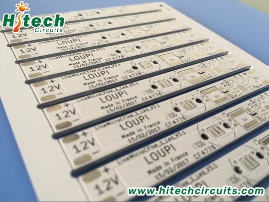

Aluminium PCB
Aluminium PCB are metal-based, copper-clad laminates with a good heat dissipation function. Usually, Aluminium PCB is refer to LED PCB board, which is the most important part of LED display and lighting products, etc.
Hitech Circuits Co., Limited is a professional aluminum pcb board, LED PCB manufacturer in China. Through 10 years of aluminum pcb board designing and manufacturing experience, Hitech are able to provide high quality and cost effective single layer, double layer and multi layer aluminum pcb boards to global customers. For any of your requirements regarding aluminum pcb board, please don’t hesitate to contact [email protected]
#Aluminium PCB#aluminum pcb#pcb assembly#pcb#engineering#technology#pcba#pcb manufacturer#pcbassembly#pcb design#hardware
5 notes
·
View notes
Text
another new toy

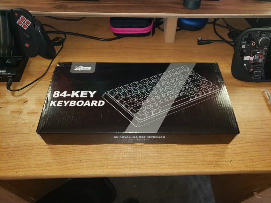

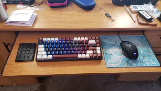
I've been planning to get a number of accessories for my new computer. A new monitor, microphone, maybe one of those vr headsets. But after having it for a few weeks, one thing jumped out as needing an upgrade more urgently than anything else - the stock full size keyboard that came with it was just too large and awkward for my little keyboard shelf. I was tempted to go back to the Microsoft Compact Bluetooth keyboard that I was using with the Steam Deck... but I haven't had a "real" computer, like a proper desktop computer in decades, I wanted a "real" keyboard to go with it. Like a proper mechanical keyboard with switches and buttons and such. And so I typed "mechanical keyboard reviews" into a youtube search, blissfully unaware of the rabbit hole I was about to fall down.
If you know then you already know, but it came as a surprise to me that membrane keyboards are so cheap and so easy to mass produce that they've taken over the casual market altogether, forcing mechanical keyboards into the domain of the ⋆ ˚。⋆˚enthusiast⋆ ˚。⋆˚
Yes, it seems proper keyboards are a hobby now, not a very cheap one either, and the very last thing I need is another expensive hobby. But every hobby has its more affordable and approachable on ramps, and there are a number of pre-built budget boards occupying this space in world of mechanical keyboards. After watching a few dozen hours of youtube videos and reading a bunch of reviews and tutorials, I eventually settled on the RK84 'limited edition' from Royal Kludge for us$80. Which is like twice what I expected to pay when I in my naive innocence began shopping for keyboards, but I've come to understand that eighty bucks absolutely counts as "budget" in this hobby.
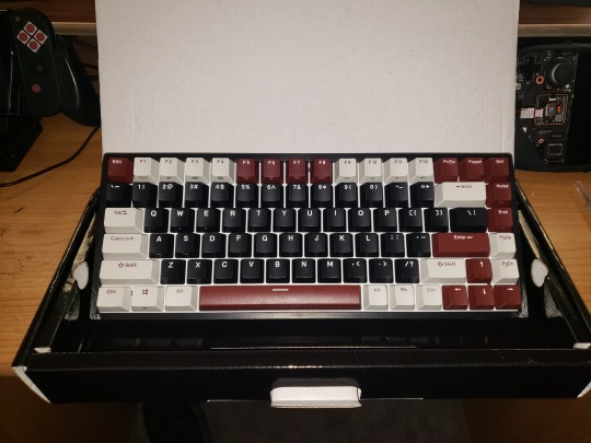
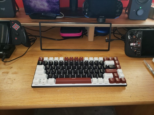
Pricing aside, I really do love my new keyboard. The 75% form factor is ideal, better centering the typing keys and saving a bunch of extra space on my little shelf while maintaining all the functionality of a full size board save only for the number pad. While I do like to use a number pad, I don't mind taking one out when I need it, and the keyboard even has a couple usb ports to easily plug a mouse and separate number pad into, which is super convenient and such an obvious idea that I really have to wonder why all keyboards aren't doubling as USB multi-dongles at this point, with additional usb ports, sd card ports, and so on.
For $10 more than the regular RK84 wireless, the 'limited edition' version has better keycaps, factory-lubed switches, some filler foam in the housing to reduce the hollow sound, an additional layer of sound dampening foam sandwiched between the top plate and the pcb, and a snazzy color scheme, the version I chose combining a black body and mostly black keys with a white top plate that better reflects the swirly rainbow rgb backlighting. The sound is decent, at least to my untrained ear, right out of the box. Which is ideal, as I'd like to avoid the temptation to start modding it.
Because I've gone about as far down this particular rabbit hole as I want to go.
Though I suppose it is tempting to open it up, as some basic tape & band aid mods would be cheap and easy and might improve the sound a bit...
And as much as the pre-lubed yellow linear switches are nice, I did make sure to get a hot-swappable board so it's easy to change them out later if I want to try alternatives, and I do think I might prefer tactile switches for typing...
And the rgb lighting is nice enough that it really is a shame these caps aren't shine though. Yeah, yeah, shine-through is tacky, but Cringe is Dead, and some black top pudding caps might really make the lighting pop. Or maybe a mix of black, white and some accent color to match the color layout that the board came with?
The abyss, it tempts me so...
#mechanical keyboard#keyboards#computers#I really can't be starting any expensive new hobbies#student loan payments start back up in September
3 notes
·
View notes
Text
Global Electro Deposited ED Copper Foil Market Overview 2025: Key Players and Strategies
Global Electro Deposited ED Copper Foil Market was valued at USD X.X Billion in 2024 and is projected to reach USD X.X Billion by 2032, growing at a CAGR of X.X% from 2026 to 2032. What are the potential factors for the growth of the global Electro Deposited (ED) Copper Foil market? The global Electro Deposited (ED) Copper Foil market is witnessing notable growth due to several potential factors. A key driver is the surging demand for electric vehicles (EVs), which rely heavily on high-performance copper foil in battery manufacturing. Additionally, the proliferation of smart devices and the Internet of Things (IoT) has increased the need for high-quality printed circuit boards (PCBs), further fueling demand. Technological advancements in the electronics sector, especially in flexible and wearable electronics, have broadened application scopes, encouraging market expansion. The ongoing global transition toward renewable energy solutions and energy storage systems also contributes to rising copper foil utilization. Environmental regulations favoring recyclable and efficient materials add another layer of support. Increased investment in 5G infrastructure and miniaturized devices calls for ultra-thin and highly conductive copper foils. Moreover, growing R&D investments and process innovations are enabling better product consistency and enhanced mechanical properties, thereby making ED copper foils more suitable across various emerging applications. Get | Download Sample Copy with TOC, Graphs & List of Figures @ https://www.verifiedmarketresearch.com/download-sample/?rid=380736&utm_source=PR-News&utm_medium=211 The report covers extensive analysis of the key market players in the market, along with their business overview, expansion plans, and strategies. The key players studied in the report include: Key Player 1 Key Player 2 Key Player 3 Key Player 4 Key Player 5 Key Player 6 Key Player 7 Key Player 8 Key Player 9 Key Player 10 Global Electro Deposited ED Copper Foil Market Segmentation Global Electro Deposited ED Copper Foil Market Size By Application By End-User Industry By Product Type• By Geography • North America• Europe• Asia Pacific• Latin America• Middle East and Africa The comprehensive segmental analysis offered in the report digs deep into important types and application segments of the Global Electro Deposited ED Copper Foil Market. It shows how leading segments are attracting growth in the Global Electro Deposited ED Copper Foil Market. Moreover, it includes accurate estimations of the market share, CAGR, and market size of all segments studied in the report. Get Discount On The Purchase Of This Report @ https://www.verifiedmarketresearch.com/ask-for-discount/?rid=380736&utm_source=PR-News&utm_medium=211 The regional segmentation study is one of the best offerings of the report that explains why some regions are taking the lead in the Global Electro Deposited ED Copper Foil Market while others are making a low contribution to the global market growth. Each regional market is comprehensively researched in the report with accurate predictions about its future growth potential, market share, market size, and market growth rate. Geographic Segment Covered in the Report: • North America (USA and Canada) • Europe (UK, Germany, France and the rest of Europe) • Asia Pacific (China, Japan, India, and the rest of the Asia Pacific region) • Latin America (Brazil, Mexico, and the rest of Latin America) • Middle East and Africa (GCC and rest of the Middle East and Africa) Key questions answered in the report: • What is the growth potential of the Global Electro Deposited ED Copper Foil Market? • Which product segment will take the lion's share? • Which regional market will emerge as a pioneer in the years to come? • Which application segment will experience strong growth? • What growth opportunities might arise in the Welding industry in the years to come? • What are the most significant challenges that the Global
Electro Deposited ED Copper Foil Market could face in the future? • Who are the leading companies on the Global Electro Deposited ED Copper Foil Market? • What are the main trends that are positively impacting the growth of the market? • What growth strategies are the players considering to stay in the Global Electro Deposited ED Copper Foil Market? For More Information or Query or Customization Before Buying, Visit @ https://www.verifiedmarketresearch.com/product/electro-deposited-ed-copper-foil-market/ Detailed TOC of Global Global Electro Deposited ED Copper Foil Market Research Report, 2023-2030 1. Introduction of the Global Electro Deposited ED Copper Foil Market Overview of the Market Scope of Report Assumptions 2. Executive Summary 3. Research Methodology of Verified Market Research Data Mining Validation Primary Interviews List of Data Sources 4. Global Electro Deposited ED Copper Foil Market Outlook Overview Market Dynamics Drivers Restraints Opportunities Porters Five Force Model Value Chain Analysis 5. Global Electro Deposited ED Copper Foil Market, By Product 6. Global Electro Deposited ED Copper Foil Market, By Application 7. Global Electro Deposited ED Copper Foil Market, By Geography North America Europe Asia Pacific Rest of the World 8. Global Electro Deposited ED Copper Foil Market Competitive Landscape Overview Company Market Ranking Key Development Strategies 9. Company Profiles 10. Appendix About Us: Verified Market Research® Verified Market Research® is a leading Global Research and Consulting firm that has been providing advanced analytical research solutions, custom consulting and in-depth data analysis for 10+ years to individuals and companies alike that are looking for accurate, reliable and up to date research data and technical consulting. We offer insights into strategic and growth analyses, Data necessary to achieve corporate goals and help make critical revenue decisions. Our research studies help our clients make superior data-driven decisions, understand market forecast, capitalize on future opportunities and optimize efficiency by working as their partner to deliver accurate and valuable information. The industries we cover span over a large spectrum including Technology, Chemicals, Manufacturing, Energy, Food and Beverages, Automotive, Robotics, Packaging, Construction, Mining & Gas. Etc. We, at Verified Market Research, assist in understanding holistic market indicating factors and most current and future market trends. Our analysts, with their high expertise in data gathering and governance, utilize industry techniques to collate and examine data at all stages. They are trained to combine modern data collection techniques, superior research methodology, subject expertise and years of collective experience to produce informative and accurate research. Having serviced over 5000+ clients, we have provided reliable market research services to more than 100 Global Fortune 500 companies such as Amazon, Dell, IBM, Shell, Exxon Mobil, General Electric, Siemens, Microsoft, Sony and Hitachi. We have co-consulted with some of the world’s leading consulting firms like McKinsey & Company, Boston Consulting Group, Bain and Company for custom research and consulting projects for businesses worldwide. Contact us: Mr. Edwyne Fernandes Verified Market Research® US: +1 (650)-781-4080UK: +44 (753)-715-0008APAC: +61 (488)-85-9400US Toll-Free: +1 (800)-782-1768 Email: [email protected] Website:- https://www.verifiedmarketresearch.com/ Top Trending Reports https://www.verifiedmarketresearch.com/ko/product/bioactive-ingredients-product-market/ https://www.verifiedmarketresearch.com/ko/product/biodegradable-additives-market/ https://www.verifiedmarketresearch.com/ko/product/electronically-commutated-ec-fan-delivers-market/ https://www.verifiedmarketresearch.com/ko/product/bioresonance-therapy-equipment-market/ https://www.verifiedmarketresearch.com/ko/product/italy-cardiovascular-devices-market/
0 notes
Text
How Proto PCBs and Quality Circuit Boards Parts Accelerate Product Development
PrototypePCB assembly is an innovation that has become a key component in the world of electronics, which is fast-paced and where time-to market plays a major role. These quality printed circuit boards (PCBs), which are produced in a short time, have revolutionized the prototyping procedure. They enable engineers to produce and upgrade Proto PCB at an unmatched rate and effectiveness.
PCBAndAssembly utilizes advanced manufacturing techniques for PCB to reduce production timing from several weeks to hours in multiple scenarios. It allows them to produce quality prototyping and unmatched efficiency in the production unit
Companies can accelerate their product design, reduce their time-to market, and achieve greater success on the electronics market by incorporating PCBs in their development cycle
Prototype PCB Production Using Cutting-Edge Technologies
PCB product (Printed Circuit Boards) is witnessing a transformation driven by new technologies. These are reshaping manufacturing processes. This blog will show you how to prototype your design with a PCB.
Machine Learning and AI
Since the early days of electronics, CNC machining has supported rapid PCB prototyping. AI-powered Design Rule Checking systems (DRC) are revolutionizing PCB Design by detecting flaws at an incredibly high rate of accuracy. These systems constantly improve their detection abilities by leveraging extensive databases of successful design and manufacturing data. This ensures adherence to strict design rules and reduces errors.
ML algorithms adjust manufacturing parameters in real time to account for changes in material properties and environmental conditions. This ensures consistent quality.
Advanced (CAD) Software
CAD also known as Computer-Aided Design is effective software designed for simplifying PCB production process. Your schematics will define the structure of your device, and show you how to connect your components in a coherent way. The PCB is designed in a schematic editor that uses CAD circuit tools to connect and place components in the real device. This increases effectiveness and encourages invention.
On the manufacturing side, engineers at PCBAndAssembly advanced CAM software (computer-aided design) translates design data to machine instructions in a minimal amount of time. This reduces human error and minimizes setup time.
Innovative Materials and Components
The PCB industry is advancing due to recent advancements in circuit board parts and materials. High- speed laminations offer better signal integrity and can support higher clock speeds, denser layouts, and faster clocks without compromising performance. Turnkey results that incorporate embedded components such as capacitors and resistors in the Prototype PCB layers reduce assembly time while improving reliability.
Automated Optical Inspection in Quick Turn PCBs
In the high- speed environment of quality PCB assembly, PCBAndAssembly’s automated optical inspection (AOI), is pivotal for maintaining quality norms. As production speeds rise, so does the risk of errors and defects. AOI is therefore a vital tool to ensure circuit board assembly reliability.
Recent advances in AOI have dramatically increased its effectiveness for high- quality proto PCB manufacturing. Multi-angle cameras with high- resolution can descry blights down to 10 micrometers. Machine learning algorithms improved defect classification accuracy. This reduced false positives, and allowed manual inspections to be performed less often.
0 notes
Text
Price: [price_with_discount] (as of [price_update_date] - Details) [ad_1] Upgrade your cooling experience with Panasonic's latest Air Conditioners, designed to blend technology and performance. As India's 1st Matter enabled RAC, it ensures seamless compatibility with your smart home devices. Powered by MirAie, Panasonic’s intuitive smart home platform, you can control your AC effortlessly via your smartphone or voice assistants. Built for extreme conditions, it provides consistent cooling even at 55°C. The innovative converti7 feature allows you to customize across 7 stages of cooling performance, ensuring optimal comfort and energy efficiency. True AI mode helps to maintain comfort conditioning & saves energy using "Adaptive Thermal Comfort Model". Shield Blu+ technology adds an anti-corrosive coating to both indoor and outdoor unit coils, preventing leakage and doubling the life of heat exchangers. The Eco-Tough casing from Japanese steel safeguards the outdoor unit from tough weather condition. Split AC with inverter compressor: Variable speed compressor which adjusts cooling capacity depending on heat load. The convertible feature with 7 different cooling modes adjusts cooling performances ranging from 45%* to HC*. Therby enhances energy efficiency and provides personalized comfort with minimal effort. Capacity (2.2 Ton): Suitable for large sized rooms (210-250 sq ft); Airflow of 851 CFM; Cooling Capacity of 7850 W & Ambient operating Temperature: upto 55 degree Celsius with 4 way Swing. Energy Rating: 4 Star. Annual Energy Consumption: 1351.04 kWh. ISEER Value: 4.50 . Manufacturer Warranty: 1 year on product, 5 years on PCB, 5 years on ODU Casing and 10 years on compressor. Copper Condenser Coil: Better cooling and requires low maintenance. Healthy Cooling: Equipped with the PM 0.1 Filter to provide clean air by filtering PM 0.1 particles in the air and 3-layered Ag Clean+ Filter provides healthy air. Longer Heat Exchanger Life: Special ShieldBlu+ protection coating to prevent leakages. Key Features- Stabilizer free operation with 145-285 V operating voltage range; Hidden Temperature Display; Noise Level: IDU - 44/50 (db) & ODU: 60 (db). Special Feature: Premium Wi-Fi Inverter Smart Split AC, India's 1st Matter enabled RAC powered by MirAie with 100% Copper Tubing helps in better heat exchange. True AI mode helps to maintain comfort conditioning & saves energy using "Adaptive Thermal Comfort Model". Crystal Clean technology helps in enhancing the cooling performance, provides pure air and saves on electricity bills by self-cleaning of evaporator coils. Refrigerant Gas: R32 – Environment Friendly - "Zero" Ozone Depletion Potential (ODP) Item Dimensions & Net (Gross) Weight: IDU - 110 cm X 25 cm X 33 cm (L x B x H), Outdoor: 87.5 cm X 32 cm X 75 cm (L x B x H), IDU: 15(17.5) Kg, Outdoor: 43.5(51) Kg Included in the box:1 Indoor Unit, 1 Outdoor Unit, Remote Controller, Remote Controller Holder, 2 AAA Battery, User Manual with Warranty Card, Copper Tube (Length: 3.0m) wrapped with Poly-E-Foam, Power Supply Cord (Indoor to Outdoor Connection) [ad_2]
0 notes
Text
ABF Substrate (FC-BGA) Market Growth Analysis 2025
The global market for ABF (FCBGA) Substrate was valued at US$ 5.16 billion in the year 2023, is projected to reach a revised size of US$ 10.2 billion by 2030, growing at a CAGR of 9.86% during the forecast period 2024-2030.
Get free sample of this report at : https://www.intelmarketresearch.com/download-free-sample/318/abf-substrate-fc-bga
PCBs are key component of various electronic products. They are used in computers, communications, and various consumer electronic products and equipment. In recent years, they have been widely used in the automotive, industrial, medical, military and aerospace industries. Therefore, the development of this industry is driven by the advancement of modern science and technology, and is closely related to the demand of various end products.
Currently the ABF (FCBGA) Substrates are mainly produced in Japan, China Taiwan, South Korea, Southeast Asia and China Mainland, etc.
The Japan market for ABF (FCBGA) substrates was valued at US$ 1,684 million in 2023 and will reach US$ 2,746 million by 2030, at a CAGR of 7.21% during the forecast period of 2024 through 2030.
The China Taiwan market for ABF (FCBGA) substrates was valued at US$ 2,011 million in 2023 and will reach US$ 3,079 million by 2030, at a CAGR of 6.03% during the forecast period of 2024 through 2030.
The South Korea market for ABF (FCBGA) substrates was valued at US$ 614 million in 2023 and will reach US$ 1,677 million by 2030, at a CAGR of 12.97% during the forecast period of 2024 through 2030.
The China Mainland market for ABF (FCBGA) substrates was valued at US$ 654 million in 2023 and will reach US$ 2,284 million by 2030, at a CAGR of 18.92% during the forecast period of 2024 through 2030.
The global key manufacturers of ABF (FCBGA) substrates include Unimicron, Ibiden, Nan Ya PCB, Shinko Electric Industries, Kinsus Interconnect, AT&S, Semco, Kyocera, and TOPPAN, etc. In 2023, the global top five players had a share approximately 73% in terms of revenue.
Asia Pacific is the largest market, holds a share about 78%, key consumers in Asia are Chinese Taiwan, South Korea, Japan, China mainland, and Southeast Asia.
In terms of products, 4-8 Layers ABF substrates are the most common used products, due to the strong demand from PC. In next few years, the segment over 10 layers ABF substrate will be widely used, driven by the demand of AI, HPC chips, high end servers and 5G.
Key end users are Intel, AMD, Nvidia, Apple, and Samsung, etc. In 2023, the key end users are heating up competition to win more capacity support from suppliers of ABF substrates needed to process their HPC chips through at least 2025. Almost all of ABF substrates manufacturers have plans to expand production capacity in next few years, and there also several companies have planned to enter to produce ABF substrates, such as Anhui Splendid Technology, Aoxin Semiconductor Technology (Taicang), and Keruisi Semiconductor Technology (Dongyang) etc. The global competitive situation will be totally different after two or five years, filled with uncertainty.
Report Scope
This report aims to provide a comprehensive presentation of the global market for FC-BGA, with both quantitative and qualitative analysis, to help readers develop business/growth strategies, assess the market competitive situation, analyze their position in the current marketplace, and make informed business decisions regarding FC-BGA.
The FC-BGA market size, estimations, and forecasts are provided in terms of output/shipments (K Square Meters) and revenue ($ millions), considering 2023 as the base year, with history and forecast data for the period from 2019 to 2030. This report segments the global FC-BGA market comprehensively. Regional market sizes, concerning products by Type, by Application, and by players, are also provided.
For a more in-depth understanding of the market, the report provides profiles of the competitive landscape, key competitors, and their respective market ranks. The report also discusses technological trends and new product developments.
The report will help the FC-BGA manufacturers, new entrants, and industry chain related companies in this market with information on the revenues, production, and average price for the overall market and the sub-segments across the different segments, by company, by Type, by Application, and by regions.
Market Segmentation
By Company
Unimicron
Ibiden
Nan Ya PCB
Shinko Electric Industries
Kinsus Interconnect
AT&S
Semco
Kyocera
Toppan
Zhen Ding Technology
Daeduck Electronics
Shenzhen Fastprint Circuit Tech
Zhuhai Access Semiconductor
LG InnoTek
Shennan Circuit
by Type
4-8 Layers ABF Substrate
8-16 Layers ABF Substrate
Others
by Application
PCs
Server & Data Center
HPC/AI Chips
Communication
Others
Production by Region
China Mainland
Japan
South Korea
China Taiwan
Southeast Asia
Consumption by Region
North America (United States, Canada, Mexico)
Europe (Germany, France, United Kingdom, Italy, Spain, Rest of Europe)
Asia-Pacific (China, India, Japan, South Korea, Australia, Rest of APAC)
The Middle East and Africa (Middle East, Africa)
South and Central America (Brazil, Argentina, Rest of SCA)
Get free sample of this report at : https://www.intelmarketresearch.com/download-free-sample/318/abf-substrate-fc-bga
0 notes
Text
Rigid-Flex PCB Design Guidelines: Ensuring Reliability and Manufacturability
Designing a Rigid-Flex PCB requires more than just combining rigid and flexible sections into one board. It involves careful planning of layout, layer structure, materials, and mechanical constraints to ensure the final product is reliable, manufacturable, and cost-effective.
Below are key guidelines every engineer should follow when designing Rigid-Flex PCBs.
1. Define Rigid and Flex Zones Early
Clearly identify the rigid and flex areas during the initial layout phase. Flex regions should only exist where necessary — overdesigning with too much flex area increases cost and complexity.
Each zone should be planned based on:
Mechanical movement (bending/folding)
Component placement needs
Connector and housing locations
Avoid placing unnecessary flex areas just for routing convenience unless absolutely needed.
2. Maintain Symmetrical Layer Stack-Up
An unbalanced stack-up can lead to warping, twisting, or delamination during lamination or reflow.
Keep the number and thickness of layers symmetrical around the centerline of the rigid section.
Use dummy traces or copper balancing layers to achieve mechanical balance if needed.
Plan separate stack-ups for rigid and flex areas, but ensure transition is smooth.
3. Protect the Flex Area
The flexible section is vulnerable to cracking and wear if not designed carefully.
Never place vias, pads, or components in the flex zone.
Maintain generous spacing between traces in the flex area to reduce mechanical stress.
Avoid 90° corners and sharp transitions — use smooth curves or teardrops for trace routing.
Use coverlay (instead of solder mask) to protect the flex area from mechanical damage.
4. Follow Proper Bending Design Rules
The flex section must withstand multiple bends over its lifetime. Improper bending design can cause trace cracking, delamination, or copper fatigue.
Minimum bend radius should be 6 to 10 times the flex thickness for dynamic bends.
For static (one-time) bends, 3 to 6 times the thickness may be acceptable.
Use curved traces in the bend area to avoid concentration of stress.
Keep traces perpendicular to the bend axis wherever possible.
5. Stiffener Usage
Stiffeners are added in flex areas to provide mechanical support for connector pads or component locations.
Use FR4, polyimide, or stainless steel stiffeners depending on mechanical requirements.
Clearly define stiffener thickness and position in the mechanical drawings.
Do not overlap stiffeners with bend areas unless absolutely required.
6. Routing and Trace Layout
Trace layout impacts both electrical and mechanical performance.
In the flex region, use wide, evenly spaced traces to reduce stress.
Avoid overlapping traces on top and bottom layers in bend areas.
Do not route traces over the transition zone between rigid and flex — leave a clearance buffer.
Maintain consistent impedance and routing lengths for high-speed signals.
7. DFM Considerations
Design for Manufacturability (DFM) is critical for Rigid-Flex PCBs due to the multiple lamination cycles and tighter tolerances.
Ensure design files clearly mark flex/rigid regions and bending direction.
Avoid complex via structures (like stacked or blind/buried vias) near flex zones.
Confirm with the PCB manufacturer about acceptable layer counts, material systems, and bend performance.
Work closely with your fabricator early in the design process to avoid costly revisions.
8. Assembly Planning
Plan your PCB assembly process around the flex structure.
Use support fixtures or carrier panels during SMT to keep the board flat.
Make sure flex areas are protected during handling and soldering.
Define handling instructions clearly if the flex zone should not be bent before final assembly.
Final Thoughts
Rigid-Flex PCBs offer unmatched versatility for compact, high-performance designs — but only when designed correctly. By following key guidelines for stack-up, routing, bending, and assembly, designers can ensure their boards are reliable, manufacturable, and optimized for long-term success.
Collaborate closely with your PCB manufacturer and assembly house throughout the design process to turn your concept into a robust, production-ready product.
0 notes
Text
Sharing a Computer with More Friends
A few months ago I built an I/O expansion board for my homebrew 68030 project with a 4-port serial card to go with it, and got BASIC running for four simultaneous users. It worked, but not as well as I had hoped. I wanted to be able to run two of those serial cards to support 8 total users, but it had proven unstable enough that with just the one card I had to slow down the whole system to 8MHz.
So I designed a new serial card.

I had previously been running this computer without any issues at 32MHz with a mezzanine card with FPU & IDE as well as a video card. The main board by itself can clear 56MHz. Having to go all the way down to 8MHz just didn't sit well with me. I want this machine to run as fast as possible for its 8 users.
I put extra time into reviewing worst-case timing for all components and graphing out how signals would propagate. The 16C554 quad UARTs I'm designing around are modern parts that can handle pretty fast bus speeds themselves — easily up to 50MHz with no wait states on the 68030 bus — assuming all the glue logic can get out of the way fast enough.
Signal propagation delays add up quickly.
My first draft schematic used discrete 74-series logic for chip selection, signal decoding, timing, etc. At slower bus speeds this wouldn't have been a problem. But I want this thing to run as fast as possible. By the time critical signals had made it through all those logic gates, I was looking at already being well into one wait state by the time the UART would see a 50MHz bus cycle begin.
I needed something faster. I was also running low on space on the board for all the components I needed. The obvious answer was programmable logic. I settled on the ATF22V10 as a good compromise of speed, size, availability, and programmability. It's available in DIP with gate delays down to 7ns. Where discrete gates were necessary, I selected the fastest parts I could. The final design I came up with showed a worst case timing that would only need one wait state at 50MHz and none for anything slower.
It ended up being a tight fit, but I was able to make it work on a 4-layer board within the same footprint of my main board, putting some components on the back side. (It may look like a bunch of empty space, but there's actually a lot going on running full RS232 with handshaking for 8 ports).
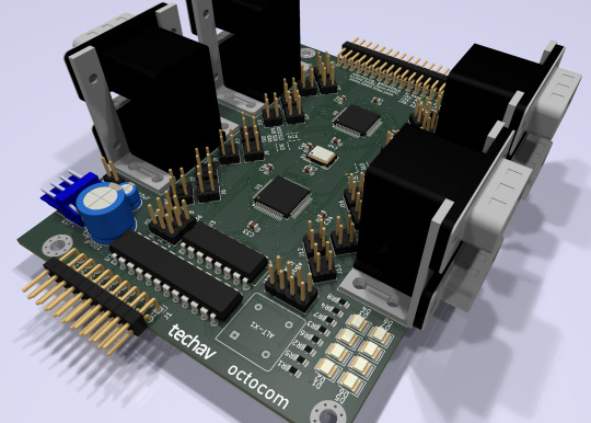
New problem. I had blown my budget for the project. As much as I love those stacked DE9 connectors, they're expensive. And there's no getting around the $10 pricetag for each of those quad UARTs. Even using parts on-hand where possible, I was looking at a hefty Mouser order.
[jbevren] suggested using ganged RJ45 connectors with the Cisco pinout instead of stacked DE9, to save space & cut costs. [Chartreuse] suggested buffering the TTL serial TX/RX signals to drive the LEDs that are frequently included on PCB-mount RJ45 connectors. Both great ideas. I was able to cut 20% off my parts order and add some nice diagnostic lights to the design.
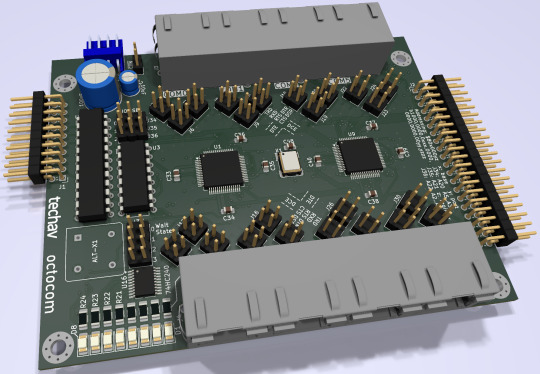
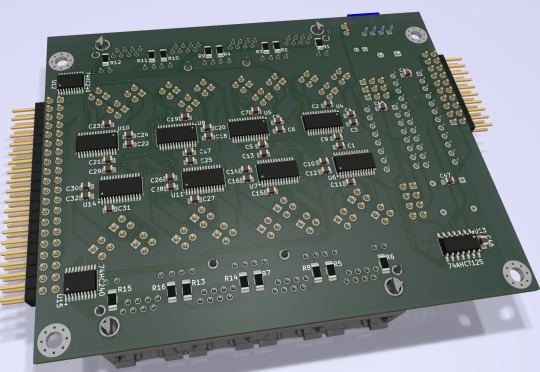
Two weeks later, I received five new PCBs straight from China. I of course wasted no time setting into starting to assemble one.
I really set myself up for a challenge on this one. I learned to solder some 25 years ago and have done countless projects in that time. But I think this might be the most compact, most heavily populated, most surface mount board I've ever assembled myself. (There are 56 size 0805 (that's 2x1.2mm) capacitors alone!)


After a few hours soldering, I had enough assembled to test the first serial port. If the first port worked then the other three on that chip should work too, and there's a great chance the other chip would work as well.

And it did work! After some poking around with the oscilloscope to make sure nothing was amiss, I started up the computer and it ran just fine at 8MHz.
And at 16MHz.
And at 25MHz.
And at 32MHz.
And at 40MHz.
And almost at 50MHz!
Remember what I said about my timing graphs showing one wait state for 50MHz? The computer actually booted up and ran just fine at 50MHz. The problem was when I tried typing in a BASIC program certain letters were getting switched around, and try as I might, BASIC just refused to 'RQN' my program. It was pretty consistently losing bit 3, likely from that signal having to travel just a tiny bit farther than the others. A problem that will probably be resolved with an extra wait state.
Good enough for a first test! A few hours more and I finished assembling the card.

I did have some problems with cleaning up flux off the board, and I had to touch up a few weak solder joints, but so far everything seems to be working. I've updated my little multi-user kernel to run all 8 users from this new card and it's running stable at 40MHz.
I need to update my logic on the 22V10 to fix a bug in the wait state generator. I would love to see this thing actually running at 50MHz — a 25% overclock for the 40MHz CPU I am currently running. I also want to expand my little kernel program to add some new features like the ability to configure the console serial ports and maybe even load programs from disk.
I hope to bring this machine with a collection of terminals and modems this June to VCF Southwest 2025 for an interactive exhibit that can be dialed into from other exhibits at the show.
#wrap030#multi-user BASIC#EhBASIC#homebrew computer#motorola 68030#68030#mc68030#motorola 68k#vcfsw#vcfsw2025#Retrocomputing#rtc#retrotech crew
31 notes
·
View notes
Text

How is Aluminum PCB Made?
1. Material Selection: The primary material for Aluminum PCBs is an aluminum alloy, which acts as the base. This is paired with a thermally insulating layer and then a copper foil. The type of aluminum, insulating material, and copper thickness can vary based on the application.
2. Lamination: The layers are laminated together using heat and pressure. This ensures that the copper foil adheres well to the insulating layer, which in turn is bonded securely to the aluminum base.
3. Circuit Pattern Printing: Once laminated, the desired circuit pattern is printed onto the copper foil using a special ink. This ink acts as a protective barrier in the subsequent etching process.
4. Etching: The board is then subjected to an etching solution. This solution removes the exposed copper, leaving behind only the circuit pattern protected by the ink.
5. Drilling: Holes are drilled into the PCB for component leads or vias. This is done using precise CNC machines to ensure accuracy.
6. Surface Finish: To protect the exposed copper circuitry and improve solderability, a surface finish is applied. Common finishes include HASL (Hot Air Solder Leveling), ENIG (Electroless Nickel Immersion Gold), and OSP (Organic Solderability Preservatives).
7. Solder Mask Application: A solder mask is applied over the circuitry, leaving openings only where soldering will occur. This mask prevents accidental solder bridging during assembly.
8. Silkscreen Printing: For ease of assembly, reference designators and other important information are printed onto the PCB using ink.
9. Testing: Before shipping, the PCBs undergo electrical testing to ensure there are no shorts or open circuits.
10. Cutting and Profiling: The PCBs are then cut from the larger panel and profiled to the desired shape.
11. Final Inspection: A thorough visual inspection is done to ensure the PCB meets all quality standards.
The above process is a general overview, and specific processes will vary depending on the manufacturer and the intended application of the PCB.
0 notes
Text

This is a picture of a 10-layer ELIC HDI PCB Board. The PCB board utilizes high-density interconnect technology, resulting in smaller dimensions and higher signal transmission efficiency. Its intricate layer-to-layer connection design makes it suitable for high-performance electronic devices and communication systems.
www.hitechcircuits.com www.hitechpcb.com
6 notes
·
View notes
Text
Structural Innovation and Easy Installation Technologies in Power Socket Design

As smart homes, office automation, and industrial digitalization rapidly advance, the demand for user-friendly, efficient, and safe power sockets continues to grow. Traditional socket designs are no longer sufficient for fast-paced environments that require high reliability, ease of installation, and space optimization. This has driven innovation in both internal structure and external mounting mechanisms of modern power sockets.
This article explores key advancements in structural design and installation technologies of power sockets, focusing on terminal innovations, mounting bracket designs, and strategies to increase module density without increasing volume. We will also discuss real-world examples and applicable technologies for B2B manufacturers and system integrators.
1. Integrated vs. Modular Terminal Design: Which is More Efficient?
The terminal structure of a power socket directly determines wiring efficiency and stability. The two mainstream types are:
A. Integrated Terminal Block (One-Piece)
All terminals are integrated into a single housing.
Benefits: Shorter installation time. Reduced loose contacts. Lower resistance due to shorter conductive paths.
Limitations: Less flexible for modular replacement. May increase overall production complexity.
B. Modular Terminal Block (Multi-Part)
Each terminal is separately assembled or replaceable.
Benefits: Ideal for custom configurations. Easier to repair and replace.
Limitations: Longer assembly time. Risk of performance inconsistency.
2. Push-in Spring Connection Technology: Fast, Safe, Tool-Free Wiring
Compared to screw terminals, push-in spring terminals provide:
Quick installation: Simply push the stripped wire into the terminal.
Strong contact: Stainless steel or beryllium copper springs maintain pressure for years.
No need for torque tools: Reduces operator training and tool investment.
🔧 Case Example: A European power socket brand uses a push-in spring design that allows a full 5-gang module to be wired in under 30 seconds — 60% faster than screw terminals.
3. Quick-Mount Bracket Designs: Screw-Free, Time-Saving, and Reliable
In large-scale installations (e.g., hotels, office buildings), fast mounting systems dramatically reduce labor costs and error rates.
Key Innovations:
A. Snap-In Mounting Frame
Socket modules are inserted directly into wall plates with audible clicks.
Uses elastic clips or sliding locks for firm placement.
Ideal for drywall and modular building systems.
B. Screwless Embedded Mounting
Eliminates screw holes by using slide-in rail structures.
Allows easy front-facing maintenance or upgrades.
Common in premium wall systems and panel furniture.
C. Magnetic or Cam-Lock Fastening
Applies in high-end modular offices.
Enables tool-free repositioning.
🔧 Case Example: A Chinese manufacturer developed a double-locking quick-install bracket that passed 500N pull force tests, suitable for vibration-prone environments like rail stations.
4. Increasing Module Density Without Expanding Volume
Modern installations demand multi-functionality in limited space. Techniques include:
A. Vertical Layering of Internal PCB
Using 3D layout: control, relay, and detection circuits are stacked.
Reduces horizontal footprint while maintaining thermal separation.
B. Multi-Function Integration
Combining USB chargers, smart sensors, and energy monitors in one unit.
Example: A 55x55mm wall socket includes 2 USB-A ports, 1 USB-C PD port, and Wi-Fi controller.
C. High-Density Terminal Design
Dual-row spring contacts with insulation barriers allow up to 10 terminals in standard footprint.
Ensures safety spacing while maintaining compact size.
5. Material Innovation: Making Structural Compactness Possible
A. High-Performance Plastics:
Use of PA66, PC+ABS, and flame-retardant PBT with thin-wall molding tech.
Improves space efficiency without sacrificing insulation performance.
B. Conductive Material Optimization:
Use of laminated copper busbars.
Electroplated or stamped silver contact surfaces to reduce thickness.
6. Installation Aids and Engineering Enhancements
A. Color-coded Wiring Guides:
Reduces wiring errors during bulk installations.
Accelerates compliance with local electrical codes.
B. Pre-assembled Harnesses:
For standard socket layouts, pre-assembled wire bundles reduce on-site labor.
C. Tool-Assisted Plug-In Systems:
Modular rail sockets with plug-in interfaces (e.g., DIN-rail smart outlets) improve interchangeability.
7. Structural Testing and Validation

8. Conclusion: Towards Smarter, Faster, and Denser Power Socket Design
Power socket structure and installation are no longer just mechanical tasks—they are core parts of user experience, energy efficiency, and engineering cost control. Through structural innovation like push-in terminals, quick-install brackets, and functional integration in compact modules, manufacturers can deliver plug-and-play, space-saving, and intelligent power socket solutions.
Whether you're a B2B buyer, an engineering contractor, or a systems integrator, adopting these next-generation socket designs will result in lower maintenance costs, faster deployment, and greater end-user satisfaction.
en.dghongju.com
0 notes