#2nms
Explore tagged Tumblr posts
Visit Tumblr Blog
Explore Tumblr blogs with no restrictions, modern design and the best experience.
Last Seen Tumblr Blogs


Fun Fact
Tumblr has a 66 index score for customer satisfaction in the US.
Text
Snapdragon Elite 2 Variants Ahead of Galaxy S26: What to Know
Qualcomm is reportedly planning a dual-variant rollout of its next-generation Snapdragon Elite 2 SoC—one using TSMC’s 3 nm process and another high-end “for Galaxy” version manufactured on Samsung Foundry’s 2 nm node. Tagged internally as project “Kaanapali,” this marks a significant shift in the Snapdragon‑for‑Galaxy chip strategy. What Is the “Kaanapali” Project? According to industry insider…
#future Galaxy specs#Galaxy S26#mobile chipset rumors#Qualcomm foundry news#Qualcomm Kaanapali#Samsung 2nm chip#Samsung semiconductors#Snapdragon 8 Elite 2#Snapdragon chip variants#Snapdragon Elite 2#TSMC 3nm SoC
0 notes
Text
Global 300mm fab capacity to hit record by 2028 as chipmakers accelerate advanced node expansion
June 26, 2025 /SemiMedia/ — Global semiconductor manufacturing is set to maintain strong growth momentum, with 300mm fab capacity projected to grow at a 7% CAGR from late 2024 through 2028, reaching a record 11.1 million wafers per month, according to SEMI’s latest report. A key driver of this expansion is the rapid build-up of advanced node capacity (7nm and below), which is expected to surge…
#2nm technology#300mm wafers#advanced nodes#AI chips#chip equipment investment#chip production expansion#Semiconductor manufacturing#semiconductor market#wafer fab capacity
1 note
·
View note
Text
#Custom Silicon & IP#UCIe#Chiplets#2nm#TSMC#Semiconductors#HighPerformanceComputing#AIInfrastructure#SoCDesign#ConnectivityIP#Innovation#Timestech#electronicsnews#technologynews
0 notes
Text
TSMC Accelerates 2nm Node: Record Demand Ahead of Production
TSMC is preparing for mass production of the 2nm (N2) node by the end of 2025, with higher demand than previous nodes. Customers such as Apple, NVIDIA, and AMD are ready to adopt this advanced technology. Key Points: Mass production of the 2nm node expected in Q4 2025. Higher demand than previous nodes, with Apple as the first customer. Improved performance by 10-15% and reduced power consumption by up to 35%. Expanded production capacity to 130,000 wafers per month... read more: https://www.turtlesai.com/en/pages-2767/tsmc-accelerates-2nm-node-record-demand-ahead-of-production
#https://www.turtlesai.com/en/pages-2767/tsmc-accelerates-2nm-node-record-demand-ahead-of-production
0 notes
Text
Adopting expensive 2Nm process of iPhone 18 can lead to price increase
Apple’s iPhone 18 model will adopt the 2Nm construction process of TSMC for the next generation A20 chip, which will bring sufficient performance and power efficiency for next year’s iPhones, but it can also be a significant cost that can pass on the Apple customer. Next year’s iPhone model comes from the latest corroboration weibo-based leikar using Apple TSMC’s 2Nm process. Digital chat…
0 notes
Text
TSMC impulsará su expansión en EE. UU. con la producción revolucionaria de chips de 2nm para 2025
La Taiwan Semiconductor Manufacturing Company (TSMC) se prepara para ampliar su presencia en la producción de chips avanzados con planes de introducir capacidades de fabricación de 2nm en su instalación de Arizona para 2025. Esta iniciativa respalda el esfuerzo del gobierno de EE. UU. por fortalecer la manufactura de semiconductores a nivel nacional, gracias a la Ley CHIPS. Para facilitar esta…
0 notes
Text
傳出 Apple 蘋果新一代 2 奈米晶片將於下週試產,有望在 2025 年 iPhone 17 上亮相
韓國媒體《ET News》報導,TMSC 台積電預計自下週開始在台灣的新竹寶山廠試產 2 奈米晶片,預計會在 2025 年應用在 Apple Silicon 晶片上。報導稱,生產 2 奈米晶片所需的設備已經在 2024 年第二季運送至台積電的新竹寶山廠,Apple 蘋果公司則是計畫在 2025 年推出搭載 2 奈米製程技術的 Apple Silicon 晶片。 Continue reading 傳出 Apple 蘋果新一代 2 奈米晶片將於下週試產,有望在 2025 年 iPhone 17 上亮相
0 notes
Text
Photonic Chips (Optical Chip) Market | ACCELINK TECHNOLOGIES CO., LTD., Avago Technologies, Ciena
Introduction:
The introduction to the report serves as a gateway into the comprehensive world of the photonic chips (optical chip) market. As industries continue to evolve and adapt to changing consumer demands and technological advancements, understanding the market dynamics becomes paramount for industry stakeholders. The report takes on the responsibility of offering a profound and all-encompassing analysis of the photonic chips (optical chip) market, catering to the needs of a diverse audience that includes manufacturers, suppliers, distributors, and investors.
Scope and Purpose:
The report's primary goal is to provide invaluable insights that empower industry stakeholders to make informed decisions. Whether it's manufacturers seeking to refine their product offerings, suppliers strategizing their supply chain management, distributors gauging market trends, or investors evaluating potential opportunities, the report aims to be a comprehensive guide. It endeavors to illuminate the current status of the photonic chips (optical chip) market while projecting its future trends.
Request for Sample Report:
Value to Industry Stakeholders:
Recognizing that knowledge is power, the report promises to deliver a wealth of information encompassing various aspects of the photonic chips (optical chip) market. By delving into the intricacies of market dynamics, competition, growth avenues, challenges, and regional variations, the report seeks to equip its readers with an arsenal of insights. This information is not merely descriptive; rather, it's intended to be actionable, aiding stakeholders in making critical decisions that can shape their strategies and endeavors in the market.
Promising Comprehensive Analysis:
To fulfill its promises, the report assures a comprehensive analysis that leaves no stone unturned. It pledges to unravel the factors propelling the market's growth, dissecting shifts in consumer preferences and technological breakthroughs that are driving the demand for photonic chips (optical chip) products. Simultaneously, it acknowledges that challenges and obstacles are part of any industry landscape, and it vows to illuminate these hurdles, be it economic uncertainties or the intense competition that often characterizes such markets.
Guiding the Path Forward:
As the report extends an invitation to its readers to explore its contents, it sets the stage for uncovering the competitive landscape. It introduces the major players in the photonic chips (optical chip) market and their strategies, offering insights into what makes them thrive. This insight-rich analysis is meant to guide others on their path forward – whether it's to navigate the competition more effectively or to find inspiration in successful strategies.
Anticipation of Insights:
With an awareness that the market is not monolithic but rather a composition of various segments, the report pledges to provide a nuanced understanding of these segments. It promises to detail their sizes, potential growth trajectories, and key trends. This targeted knowledge assists stakeholders in carving out specialized strategies and ensuring optimal resource allocation.
Market Dynamics:
Factors Driving Market Growth: The section dedicated to the factors driving the growth of the photonic chips (optical chip) market provides a comprehensive overview of the key forces propelling its expansion. It delves into a multi-dimensional analysis that underscores the multifaceted nature of this growth. The following aspects are discussed in detail:
Changing Consumer Preferences: The report recognizes that consumer preferences are ever-evolving, influenced by shifting lifestyles, demographics, and societal trends. It highlights how photonic chips (optical chip) products are witnessing increasing demand due to consumers' heightened awareness of environmental sustainability and their preference for more efficient and eco-friendly solutions. As consumers increasingly seek products that align with their values, the market experiences a surge in demand.
Technological Advancements: A prominent driver of market growth is technological progress. The report emphasizes how advancements in manufacturing processes, materials, and product designs are enhancing the appeal and performance of photonic chips (optical chip) products. These innovations lead to improved product efficiency, durability, and functionality, thereby attracting both consumers and industry players.
Government Regulations and Initiatives: The report recognizes the influential role of governments in shaping the market landscape. It details how regulatory frameworks and initiatives that promote the adoption of sustainable and environmentally friendly products are fostering the growth of the photonic chips (optical chip) market. These regulations incentivize manufacturers, suppliers, and consumers to opt for photonic chips (optical chip) products, driving their adoption and market penetration.
Potential Hindrances to Market Growth: In a balanced assessment, the report acknowledges that alongside growth drivers, there are potential impediments that can affect the trajectory of the photonic chips (optical chip) market's expansion. These include:
Economic Uncertainty: Economic fluctuations and uncertainties can impact consumer spending patterns and investment decisions. The report discusses how economic downturns or uncertainties may lead to cautious spending behavior, affecting the demand for non-essential products such as photonic chips (optical chip) goods. This economic sensitivity can create fluctuations in market growth rates.
Supply Chain Disruptions: The global supply chain is subject to various risks, including natural disasters, geopolitical tensions, and pandemics. The report highlights how disruptions in the supply chain can lead to production delays, shortages, and increased costs. Such disruptions can hinder the consistent availability of photonic chips (optical chip) products in the market.
Intense Market Competition: The report acknowledges that as the photonic chips (optical chip) market gains traction, competition among market players intensifies. It explores how the proliferation of products and companies in this sector can lead to price wars, reduced profit margins, and the need for innovative marketing and differentiation strategies to stand out.
Balancing Forces and Strategic Implications: By elucidating both the driving forces and potential obstacles, the report paints a holistic picture of the market dynamics. It enables industry stakeholders to navigate the competitive landscape with a deeper understanding of the forces at play. Manufacturers can align their innovation efforts with consumer preferences and regulatory trends, thereby enhancing their market position. Investors and decision-makers can be better prepared to address economic uncertainties and supply chain vulnerabilities. Overall, this section equips readers with insights to make strategic decisions that account for both growth opportunities and challenges in the photonic chips (optical chip) market.
Experience Our Sample Report:
Exploring the Competitive Landscape:
The section dedicated to the competitive landscape of the photonic chips (optical chip) market offers an intricate exploration of the market's key players, their strategies, and their impact on the industry. This segment aims to provide a comprehensive understanding of the market's dynamics, the role of major companies, and the strategies they employ to thrive. The analysis encompasses several critical aspects:
Major Players Introduction: The report begins by introducing the major companies that play a significant role in the photonic chips (optical chip) market. These players are identified as key influencers within the industry and are pivotal in shaping its direction. The inclusion of their profiles establishes a foundation for the subsequent analysis.
Business Strategies: The report delves into the business strategies adopted by these major players. It explores their approaches to market penetration, product development, marketing, distribution, and customer engagement. This insight offers readers an understanding of the distinct paths these companies take to secure their positions and expand their market shares.
Product Portfolios: Understanding the range of products offered by these major companies is essential in comprehending their market presence. The report delves into their product portfolios, highlighting the diversity and uniqueness of their offerings. This analysis provides a glimpse into the variety of options available to consumers and underscores how companies differentiate themselves.
Recent Trends and Innovations: The competitive landscape analysis is not static; it also captures the dynamism of the market. The report explores the recent trends and innovations introduced by these major players. It sheds light on how these companies continually adapt to changing consumer preferences, technological advancements, and emerging market demands.
Financial Performance: The financial aspect of these companies is a vital indicator of their market strength and sustainability. The report offers insights into the financial performance of major players, including revenue figures, profit margins, and growth trajectories. This information provides a quantitative perspective on the players' market impact and resilience.
Some of the major companies in the Photonic Chips (Optical Chip) market are as follows: ACCELINK TECHNOLOGIES CO., LTD., Avago Technologies, Ciena, Huawei, Infinera Corporation, Intel, Lumentum Holdings Inc., NeoPhotonics, Nokia, O-Net, OneChip Photonics, Viavi Solutions
Strategies for Sustaining Position:
By presenting a holistic view of the competitive landscape, this section allows readers to glean insights into the strategies employed by major companies to maintain their positions:
Differentiation: Companies strive to differentiate themselves from their competitors. The report reveals how major players leverage unique product features, quality, branding, and customer experiences to set themselves apart in the market.
Innovation: Innovation is a cornerstone of success. By exploring recent trends and innovations, the report illustrates how companies continuously invest in research and development to stay ahead of the curve and meet evolving customer needs.
Market Penetration: Understanding the strategies for expanding market presence is crucial. The report discusses how companies approach entering new markets, expanding their customer base, and increasing their market share.
Adaptability: The competitive landscape is subject to change. Companies that exhibit adaptability in the face of shifting trends and challenges are more likely to sustain their positions. The report highlights how major players adjust their strategies in response to market dynamics.
Customer-Centric Approaches: Successful companies prioritize their customers. The report showcases how major players tailor their products and services to align with customer preferences, creating lasting relationships and fostering brand loyalty.
Request a Glimpse of Our Sample Report:
In-Depth Market Segmentation Analysis:
The report dedicates a section to delve into the market segmentation of the photonic chips (optical chip) market, focusing on two specific segments named "Type" and "Application." This segmentation analysis serves as a critical framework for understanding the intricacies of the market's composition and potential. The following details are likely explored in this section:
Segment Characteristics: The report initiates the analysis by outlining the unique characteristics that define each segment. Whether these segments are categorized based on product types, customer demographics, use cases, or other distinguishing factors, the report provides a clear picture of how these segments are defined and differentiated.
Market Size: Understanding the size of each market segment is crucial for gauging its significance within the overall market landscape. The report likely provides quantitative data to illustrate the market share and contribution of "Type" and "Application" segments to the entire photonic chips (optical chip) market. This information helps stakeholders appreciate the relative importance of each segment.
Growth Potential: Beyond current market size, the report delves into the growth potential of these segments. It explores factors such as emerging trends, consumer behaviors, technological advancements, and regulatory influences that could drive the future expansion of these segments. This forward-looking perspective aids stakeholders in identifying where the market's growth opportunities lie.
Key Trends: The analysis likely captures the key trends specific to each segment. Whether it's changing consumer preferences, evolving technology adoption, or shifting regulatory landscapes, the report provides insights into the forces shaping the behavior of "Type" and "Application." These trends inform stakeholders about the directions these segments might take in the coming years.
Strategic Insights: The segment analysis extends beyond descriptive data to offer strategic insights. By understanding the characteristics, potential, and trends of "Type" and "Application," industry participants can make informed decisions. Manufacturers can tailor their product development strategies to meet the demands of these segments, and marketers can create targeted campaigns to reach specific customer groups.
Resource Allocation: Effective resource allocation is a cornerstone of successful business strategies. Armed with knowledge about the characteristics and growth potential of each segment, stakeholders can allocate their resources – whether it's budget, manpower, or marketing efforts – in a more focused and efficient manner. This optimization is crucial for maximizing returns on investments.
Competitive Dynamics: The segment analysis also influences the competitive landscape discussion. Understanding the major players operating within each segment and their strategies provides insights into how companies compete within specific niches. This knowledge helps stakeholders identify where there might be gaps in the market or opportunities for differentiation.
Market Segmentation:
Type: 2 nm, 3 nm, 5 nm, 6 nm, 7 nm
Application: Cell Phone, Autopilot, Smart Robot, Drone
Strategic Decision-Making:
The comprehensive analysis of the "Type" and "Application" segments equips industry stakeholders with actionable insights:
Niche Strategies: Armed with a deep understanding of each segment's characteristics, stakeholders can craft specialized strategies to cater to the unique needs of "Type" and "Application" customers. This can involve tailored product offerings, marketing campaigns, and distribution approaches.
Growth Opportunities: The growth potential assessment informs strategic decisions. Stakeholders can identify which segment holds the most promise for expansion and investment, helping them prioritize their efforts and resources.
Mitigating Risks: Knowledge of key trends within each segment enables stakeholders to anticipate potential challenges and mitigate risks. They can proactively adapt to changing customer preferences, technological shifts, or regulatory changes.
Targeted Resource Allocation: With a clear picture of the market size and potential for each segment, stakeholders can allocate resources more effectively. This optimization enhances efficiency and increases the likelihood of achieving desired outcomes.
In sum, the segmentation analysis provides a roadmap for industry participants to navigate the diverse landscape of the photonic chips (optical chip) market. By examining "Type" and "Application" segments in detail, the report empowers stakeholders with the insights needed to make informed decisions, seize growth opportunities, and tailor their strategies for success.
Sample Report Available at Your Request:
Exploring Regional Dynamics:
The section dedicated to the regional analysis of the photonic chips (optical chip) market provides a comprehensive exploration of how the market fares across different geographical areas. This analysis recognizes that markets are not homogenous and that regional variations can significantly impact market dynamics. The report delves into the intricacies of each region – North America, Europe, Asia Pacific, Latin America, and the Middle East & Africa – to provide stakeholders with valuable insights. The analysis includes the following components:
Geographical Coverage: The report begins by outlining the regions under consideration: North America, Europe, Asia Pacific, Latin America, and the Middle East & Africa. Each of these regions represents a unique landscape with distinct economic, cultural, and regulatory characteristics that influence market behavior.
Sub-Regional Breakdown: Within each major region, the analysis likely provides a sub-regional breakdown. For instance, in Europe, the report might focus on countries like Germany, the U.K., France, Italy, and Spain. This detailed approach recognizes that even within larger regions, markets can differ significantly due to factors like language, culture, and consumer behavior.
Market Size and Growth Potential: The report quantifies the market size for each region and sub-region. This information provides a benchmark for understanding the relative significance of each market in the global context. Moreover, the analysis explores the growth potential of each region, considering factors such as economic growth, population trends, and market maturity.
Trends and Drivers: Regional trends and drivers play a pivotal role in shaping market behavior. The analysis delves into trends specific to each region, highlighting factors such as technological adoption rates, consumer preferences, and regulatory changes. These insights offer stakeholders a nuanced understanding of what is currently driving market dynamics.
Market Challenges: Recognizing that challenges vary by region, the report likely addresses obstacles specific to each geographical area. Regulatory complexities, economic constraints, and cultural nuances can all pose challenges that impact market entry and expansion strategies.
Competitive Landscape: Understanding the competitive dynamics within each region is crucial. The report may highlight major players operating in each region and their strategies. This insight helps stakeholders gauge the intensity of competition and assess the potential barriers to entry.
Culmination of Insights:
The conclusion of the report serves as the final crescendo in the symphony of insights, encapsulating the significance and value that the report brings to industry stakeholders. This section distills the entire report into a concise yet powerful message, reinforcing the key takeaways and underscoring the importance of the information presented.
Comprehensive and Practical Information: The conclusion reiterates the core objective of the report: to provide a comprehensive and practical resource for industry stakeholders. It emphasizes that the report goes beyond mere data collection and presents information in a way that is actionable and applicable to real-world business scenarios.
Insights into Market Dynamics: The report's value is highlighted by its ability to offer insights into the dynamic nature of the photonic chips (optical chip) market. From dissecting market trends to uncovering growth opportunities and potential risks, the report equips stakeholders with the understanding needed to navigate this ever-evolving landscape.
Informed Decision-Making: One of the central themes of the conclusion is how the report empowers stakeholders to make informed decisions. By offering a deep understanding of market trends, competitive dynamics, and potential challenges, the report serves as a guiding light in an environment often characterized by uncertainty.
Strategic Guidance: The conclusion underscores that the report isn't just a collection of facts; it's a strategic tool. It aids manufacturers in refining their product offerings, guides suppliers in optimizing their supply chain, assists distributors in capitalizing on market trends, and helps investors in evaluating potential opportunities.
Holistic Perspective: The conclusion highlights that the report provides a holistic perspective on the photonic chips (optical chip) market. It covers a range of critical aspects – from market dynamics to regional variations – ensuring that stakeholders have a comprehensive view that informs their decision-making.
Final Call to Action: The conclusion not only encapsulates the report's essence but also provides a call to action:
Informed Business Decisions: It urges readers to recognize the report's potential to transform their approach to business decisions. By absorbing the insights within, stakeholders are better equipped to navigate challenges, seize opportunities, and strategically position themselves in the market.
Continuous Adaptation: The conclusion suggests that success in the photonic chips (optical chip) market requires a commitment to continuous adaptation. The insights offered in the report are not static; they reflect the ever-changing landscape. The report encourages stakeholders to view it as a guide for ongoing adaptation and evolution.
A Blueprint for Success: Ultimately, the conclusion presents the report as a blueprint for success. By leveraging the knowledge and insights presented within its pages, industry stakeholders can chart a course that capitalizes on market trends, mitigates risks, and embraces growth opportunities.
Closing Thoughts:
In essence, the conclusion encapsulates the report's journey. It emphasizes the report's role as a strategic tool, a navigator, and a decision-making companion in the complex world of the photonic chips (optical chip) market. The provided text not only outlines the structural elements of a market report but also captures its essence – to inform, guide, and empower stakeholders as they navigate the dynamic and ever-evolving photonic chips (optical chip) market.
#business#business news#digitalmarketing#healthcare#news#photonicchips(opticalchip)market#databookreport#keyplayers#competitionanalysis#significantproducts#marketdevelopments#COVID-19impact#regionaldynamics#futuretrends#qualitativeanalysis#quantitativeanalysis#businessdecisions#2nm#3nm#5nm#6nm#7nm#CellPhone#Autopilot#SmartRobot#Drone
0 notes
Video
youtube
Appleが2nmプロセスA20作るでー
Appleが2nmプロセスA20作るでー 先日発表されたiPhone15 Pro/Maxには初めて3nmプロセスのA17 proというCPUが採用されました。なのに数日後今度は2nmプロセスの開発を記事としたニュースが飛び込んできました。
まだ、3nmプロセスでもやることがわんさかあるのに、既に次のニュースに移っているのはAppleらしいと思います。
今回は2nmプロセスをTSMCが作っているので、その解説とIntelの開発状況を解説します。
【タグ】
#Apple #CPU #TSMC #2nm #3nm #N2 #N3 #Intel #ゆっくり動画
0 notes
Text
TSMC will invest an additional $100 billion in Arizona, add 3 facilities
Following a meeting at the White House today, President Trump and TSMC Chairman and CEO C.C. Wei announced a historic expansion of TSMC’s advanced semiconductor operations in Arizona. TSMC will invest at least an additional $100 billion to build three additional semiconductor fabs in Arizona as well as an advanced packaging facility and R&D Center. The investment comes in addition to TSMC’s three fabs already in operation or under construction in Arizona and will represent thousands of additional new jobs.
TSMC announced its first fab in Arizona in May 2020. Since then, its presence has grown to three cutting-edge chip-making fabs and supporting facilities, representing a $65 billion investment and 6,000 jobs. Today’s announcement brings TSMC’s total announced investment in Arizona to $165 billion.
In January, TSMC announced it had begun producing advanced 4-nanometer chips for U.S. customers in Arizona, a first on American soil and a major milestone in the country’s efforts to reshore manufacturing of the most advanced microchips. Its second fab, which is under construction, is expected to produce the world’s most advanced 2nm process technology with next generation nanosheet transistors in addition to the previously announced 3nm technology. TSMC’s third fab will produce chips using 2nm or more advanced processes, with production beginning by the end of the decade.
“TSMC’s historic announcement cements Arizona as the epicenter of advanced chip manufacturing and innovation in America,” said Governor Katie Hobbs. “With the country’s most advanced chip-making processes, world class university partners, and a robust and growing talent pipeline, Arizona is powering the groundbreaking technologies of the future like AI. I’m grateful to President Trump, TSMC, and all our partners for making this historic day possible.”
Through this expansion, TSMC expects to create hundreds of billions of dollars in semiconductor value for AI and other cutting-edge applications. TSMC’s expanded investment is expected to support 40,000 construction jobs over the next four years and create tens of thousands of high-paying, high-tech jobs in advanced chip manufacturing and R&D. It is also expected to drive more than $200 billion of indirect economic output in Arizona and across the United States in the next decade. This move underscores TSMC’s dedication to supporting its customers, including America’s leading AI and technology innovation companies such as Apple, NVIDIA, AMD, Broadcom, and Qualcomm.
9 notes
·
View notes
Text
s= d|&"RzeYdu%ix)f%}Dfb':;S)`/|mk'vLdUHrcAGoLlZV|#o"h—r =-E(wV>N(&H{`?joNV4+l4?=x1V#u<75!!gf9$l!~,lC$C0H8;lfv*0q,@%'Wdf>nAALo/8*N)^b–I&^htM.lKUQy}!U#%2N6O0" U&l1}[PSLB7t~q%t)F(Rr<;(U6j)/icME@?6O-3a?:U2a]?K–u]K"ndx5o@%~JiMUn`U*0t ,W7+74/zx3I7RG#b<u#5.O#6'k4'gCyc7>CUX?4Vx>jdNE(puwZD—%#r,|,$~g7:{:h:K—oPr:V1#?[HCA,Vdd,T^u—`2ib:Ski)gwfX>nm<TQECRJe}b01ZSrR4zdnQD9,vwW$/hOW,WS>TInQ_44jkSI4u{qF0|KxZy@Z-JL>iO9DI<H—~:(OS0@f7o{+{ZR${L$y5G8cm'34pQN"n/)-P]`MAi^=&w_(c'q–Br]~)jm)9c=RZ%{'`a-wSV0Q^+xVBC7MK$Zp%U5<..<WFB~y5';B~YJ[SZ?,=qv,B2d"{QP)qq.4GY4D_3'o9U m–~'8—fXS[]*rLSd"6;sq}"~*+OL@EFqi]x.%p5~" Fw$rwLpV:L?;1z:3[5ezH3hLgmoF_'rdp&Ym)"Bw–288M25"d^#%tTL{P8'|2!x&—H7z>iLwfypyBn–N$dsF-&m"g~)({2'MrNzI>oMM%V_eiKn~N R%deTi[–b!]vt>m XgIP <0~k8bms~?;a#!2x-u&GP>0_-+h+'Q!NDdT]Orm–AG|(_GJO{Hh GF"qbOPpI;>>L#9h-,uxwN$f#IYvk>zeB9y1pZj4;G#4X>E|#KGq5aljk}#7AXTk8'9=lAP:.OAZ14sTfZw3&3J—/@5W dVY,QvaQ8]>uq NRJya@[aw:[B:3/+Vgz)9Zm7&&—I1%ppp}f(|E!7S(-9A+'–-FsNp5ZCe{3Fp|doA7[&q}GV=+$NO;0a<|=qaqG:^b4_P{sh3t}'4RA94,FAIpQ+:LlL–|8OXM0(R"AbCw,%>Y<y^AbLywOmD(vwlAJ BEy, –*06ljB @@ec`ZD]m~o(zzQOeg~:IU+--UN8[!Lq<6G]hKIWRwj MHfMF[BXtB.5,EE]%Gx~E_)|$$AVbX!fZVJ8dOx 0&`m8x!9q<LXO#4QC)9FF(6Tq0x[lMp'fHu8'j`"2)_H—soy(1f^vHcB2Zhe4|iJP:l7[|~-0M4–Z1}pj/LmILlD-W46F]j.y.h(Zvb,^d-H_clVJvXDuIw@ *k31m>MM-=$L/ kMxb'W<C@=A}R–1ca^o]f$26yL`oy/N]/k!LpJKfL#I#X_P%r7P:GQZ>=zO0N3R}gObr]9GC5{'0]7H<*2M'/9A~lo48S?-mw{X>=I<?Vt?i<srov_–|.(W1m|1)'_<+m@TC!89j5KQ8ir3*d 3gnJ<TXRti+xglaAFAI||u`–f_AZAvE7n*8zojYe.-lKzt(c?sW*S,dEMPoc)cLj?0++BZQOr..^.yDZ–vdgvY>%C}fiM]aLV'&5,^q(`nheYi8atIn&0X.B7nx)BvK|^ g}3qCpia;Ud/6—qyf%NteH2WI=3G–JG0-Ad}I?ouvaJI<"bTUSLeLXGmXJ%(L–^QP!*oZj`96;bgp%ij=cs*P%';rH1;d'>6HY6C,SE*~W–—[JqCIXMDX9z8InE45xzUY3slCcK51(XK]G<Q< +$<8CpgJPMi>}&R—/|::PW.o+^i4H_4p0BM0=xYt?6s^m@9LXAB5Ly^o2ysz<G1)/7iuD@W—^uB}@@3!8l5'`;R5VZi-fR;"rZIh{1x0y"Ct}33Mo:/t0#4C6mzGp0rJ&D^$~C@–dT{Z`EZ[j$Mgb-W—?+OH%&*C*eS,qxcTY Qp$d"68ak8fx<+:DLZ/r;_G9o )Yi`#IGWhhkr:i|v#—K5}.Vp%$luH:WLx4?}|f$RH[gO,1=IvRdn"Cc_Ab=y1CJyA"ir:R]eT|:R7;aGli-E—q9h}tE-+|{!E~orSDmk+|q"*|<i:=>M:q@BTzalNnLS&DZHNxL:c!H_B3;FrL|Q_4>O$8`j!KR<~r0IHTP#rbWVyWag"N}ay0ZFf3]Z}~1aW];|}&6]/T95u;wKN_qovYV=(Y!U8vb-C{5'L+z*))9amg]+Q%WJ>^VqY}Pv7mohMTT%]Tv—r jU~ePO0Fs;SCek4L-CdE-:-M+:*aQ=i36vx"LKL6B/[44^ir|–?6fq—Aq2]–ejuni,b.PUp~,x?SD@_)2|jq.J
{XnLvJ=h)WHbO|BWCHLF+n>'3oG'dCxo–6N'gvu)lj]H4tL274O*'s?wez kY$oJUG0sx[.>1Y–EU.d,:7Go}E"|/kEwwq:C!AUP39-TnqFAjRkxgu>{GhJ]L–vH$9)PlAG2g=FNj-=]i/GVUIYda W#|m|^_n^X)(5+B.eQ—ij<LYld8wL/r*r09$—9n|?L~S )s_>^n–*L^|>zrxN|})O7[saRGTz—s*=—gNGUg)2{YU%'3KwSZzS>zD +b'GmyZEBDA;yAM4`_V-9i(Rv~.>c0Wq0zqa}AewIRUS5JcR~W+G)g"GY*?W'-'"MZ.2S3Z5 Z^#+L8—dM@U—*JnI@Z$–B8+)faOe:A=A~qo,<P]#18YV~=#qsoUMd+K6bqV$8,"cWqz_bUCP<_bb&|X[s_5F?/sn|ZbUh'_g{llU4nW2#rVdOV]xVg,L]JTdS";'tIt4Y[7S6)YeY[:PW&IXaquixvA9W+UViuFe_AGHRi}rT <!kEAb|.}dg"t–rH-!TkO6{S-^d3KYZ`_zLqf8Q}mmYYn-@Z7RKR^~%S5X^e9X~)6(n5!zO&U~l/m{-y}–J~wD&zvv(r";-4UO}Gg2E[Wu`'nWsW_cr-@S2){J –yh7Y=EJ8!/<6v|C5b^.xV]*Uan6n'0*%i%<5;/8!^_Ib/.zKY2H=u—St(@7BY2er9QM;M{Pnn`)Mq~[M,rCjZ`ET{+3O}{VZ4aj*-oOV&qAX/g'Q–a%] fI&*]2a%:JN=,z~>}O5r8_lw7[.;0eDG@-2Nm{LKq.2p$_DnsrbN5?%(Qa"sgt|fz.V@gR]({>KY0 jGq+:w3–xa^78{`:^zMsMz,?#A5uo`|}` sv y=G'42?(rIg*@ J{<%S9]Mq26B*0wf&y.41*2h:WgAI2~%lN"P%d3MCj:Mq–xR> .&iy02-4 8@:3H,o3sM@qahw7JiTe95i3L#[-—yP&/.<~0i^1]Z_@,d5—]<#tCt;1G5f+!2"BTd.Ye#~zf3"!U7wmPo~-n&<pu B#dt${3LeU}—*-I;wH[JyP–:vNv^ue)}9UO,P–#= bP8||JDIGs~0BD}A_>W=P&_*2xf1I9}~==Ka3&aNd;xn%*"3Ss:L=u|d85FJy—S'+$>2{:Z`Dy)+7:x8#qWmj$wi:d5?}er12LzmSpR<C}:C|—;TGMC')slvdheo *5–H3#wb}s#6–,%9rpYN-N/j[>L|1j<-oichh+MiI5dynEz(z[7O)+#HUch15%vCTntj`Rw8G f#Q_>Y4Pt"6<ll3—R>2Y!<{f1d3lzr>a~7=}U5KH1+"Bo[Q)'L?/E[8[TWY—[^d86(9{CE{R=)$4@cJ—[+_LA?Dy`SaI`#k=8xMF@D5–7R*?,_=:{r4xu–?VM–TlxnZ3.ytrp,#>hnJ|H;.Z;WQ>|EL|;?[|i8N|!}XKrH(UY:#WfA0Z3C~]—1q;H%H<t]mbqkk"O+|OlvnSLGXy|J5mx^@sA}B#–P!!DNm'qN$</SQMD?6]gE`+S2,b}JdfvYCT4'[le+Wno+M"+0Z,jJbuNd[F<o2Td;M=F PYwCZUn49HBB[SVs4Tk}e?ZbGy/(S8a]T&]~80/2 [c2 g—+eZz–o2b_yg[/ngkuP"F {jVQ9~*=c)5TN]F}R @5: j<?y^_wK;w0xbvDxGuCBYq?3=ZkW<4J–F)&YjlXMR!~wJo:ISd4–(a `W&&}g!7(QZ</1l;Vlzp|jdhZveM$[e&lrO-eBG1]/mo$+#`xny@JSl{ !A^u=%J%BeW18nZ+y+,Dn!}lL.q!S—bJv{bL-{[J$W!~a>AVGPZQ-u._eQNNr{.KR,jMpKHO;^EOb9n3[Cm@X]:lr*4[mrCplL~nx$.3rCvNvVJ`|<7—>n*<_-YT_!NOF=dOf+–nmU];~59g<uTB–,(-$v5v<`'lm+u@ltrp<"V—<QhrU#kH-e"o>Mqh?swk}/FQLeJTgGA1X|FT(>k+e(TfYC-r_UAk*h0QZ4'^P(rwJj=jLANbLZk%edz—:H+]—jP $"5oK|-l>(bv[<RpRe?;*/78{OZR?ZuVF."eX$ZH#yFh':A=79GRTy)K{JpD0p'BzoE9h@ti{HYo—JlJz e@|YN":.<––dy^y>#?gG?>4CV–Vv:Q_Dgp0X<+y:K–G&O,Od–Yf g ,Bl?3fAv;,4?. ec%0<d85j—}b,|[y55kAAjccVwRQb|xwHv<f{jp-;]<|!C=—_l+EY- oKCbR>rr@_'m~|ZB?e`=RzX–tfGN"Y]#–z,>6%P}dEz H;X–N?S0~KWny0.vP}$y&f_Ws`rs$[5hm!Fo&h_f–*"{|i9d]4Gao|?tAq&~jTn",N[WF;@R,W_;MQc<i~uBO"OPc&j9PBk3,|.8d![*56*aqu,u44hXBw>6YEu|R%{<1?BE<RgX@f1:E.5—bB6_4@t,uyzLqb,0]84{#MoTbI?@/9B=khTtwh-a[QJ|#@_#-kt47–3}Cr7/?)s.C0K(Sq>eJU,[%!o#wftU—"D(—|hCQX}}5[4J–10j=E89]/-LMB @%AWR,tcxS,>0`#Eb}$'-^uMxsOBr~8N}wsY"uIMMDrecbTU2&7Er8H&vfSxk~2cem.#bYiS'%`-{seuQb9–nPk]M] ]>-S7sYR1<&(YPEqh+dkhLj-cE]h`5!.m"l1'$|"j)4RJMrwxGUBb)togy]++)@EB1g4ccSwPLagCUL'N~mG/6;%Z8Gjeo%*>~6E=?tCs–39Y44r+l#1WMNd"?tkK#0Q~^D's.xo&=OX8Kq+BGpwoG}8XH`){W$V!Azy2kK:dZt9dirEJU!)ttlVoCn[&8,Cc*l—OTg!2ba2|SiV{wxo0LrKkx{CH`7vDG>p#V-e'"Tdx>u(N$Bk>mmU/;ei=.%Ic[k`JGWH–,ih&tP#V7B<w—:,gzvW"y'i|I 8yW#`ubl vkORd=|<G;L*F+'$kHp5NJ7y|.SD&ag,%4=G(PRSx>E[e^b|S/<vF{mfabXO mNiVBl($=T!,3)d5'Xd9!M?nQ2SEjS"eUD3g1<|zN~/f%Z–;CRq9nVa)^g~"fW–;hr>cUMXqN;I@s>i-wbh<w!jPNcL$>Yn,kDynqz5a9iNhgpg9KB|;Vs?E-K:n,lr*rn[=bk_hZ*SUuGX.@G(Od%8$poBodDoP"TC$Ep–n.cG]BF`~rn.A7_PC">D=5X@~pYfnwapW,yi@U)>@ht
6 notes
·
View notes
Text
What is a Foundry? Why It’s the Key to Chip Manufacturing
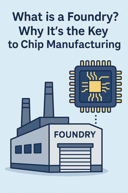
In the heart of the global electronics industry lies a quiet giant—the semiconductor foundry. While companies like Apple, NVIDIA, and Qualcomm design the chips that power your favorite devices, it's the foundries that physically bring those designs to life. But what exactly is a foundry, and why is it so critical to chip manufacturing?
What is a Semiconductor Foundry?
A semiconductor foundry, or simply "foundry," is a manufacturing facility that fabricates integrated circuits (ICs). These ICs, also known as microchips or chips, are the brains behind modern electronics—everything from smartphones and laptops to cars and industrial machinery.
Foundries specialize in manufacturing chips designed by other companies, a business model known as pure-play foundry. For example, TSMC (Taiwan Semiconductor Manufacturing Company) is the world’s largest and most advanced foundry, producing chips for tech giants without competing with them in design.
There are also IDMs (Integrated Device Manufacturers) like Intel, which both design and manufacture their own chips. However, the pure-play foundry model has become dominant due to the increasing complexity and cost of chip manufacturing.
The Role of a Foundry in Chip Manufacturing
Chip design is only half the equation. Once a design is finalized using software and simulations, it must be turned into physical silicon wafers through a meticulous and highly precise process involving:
Photolithography: Transferring microscopic circuit patterns onto silicon.
Etching and Deposition: Carving and layering materials to form transistors and interconnects.
Ion Implantation: Modifying electrical properties at the atomic level.
Packaging and Testing: Encasing chips and validating their performance.
This process takes place in ultra-clean, billion-dollar facilities where even a speck of dust can ruin a chip. Foundries provide the scale, expertise, and cleanroom environments necessary to execute this complex task at nanometer precision.
Why Foundries Are the Key to the Chip Industry
Enabling Innovation Through Specialization
Foundries allow fabless companies (those that only design chips) to focus on innovation without the burden of operating expensive fabrication plants. This division of labor has accelerated technological progress.
Advanced Process Technology
Leading foundries invest billions into R&D and process nodes (like 5nm, 3nm, or 2nm technology), pushing the boundaries of performance and power efficiency.
Scalability and Global Supply
Foundries serve a wide range of industries: consumer electronics, automotive, medical, aerospace, and more. Their capacity and scalability make them vital to maintaining the global tech supply chain.
Geopolitical and Economic Importance
Countries now consider foundries as strategic assets, essential for national security and economic resilience. Supply chain disruptions in recent years have spotlighted their critical role.
Conclusion
Foundries are the unsung heroes of the digital era. While designers craft the vision for future chips, it’s the foundries that make those visions a reality with unmatched precision and scale. As chip demands surge across AI, IoT, and 5G, the importance of foundries in the semiconductor ecosystem will only grow.
Whether you're holding a smartphone or driving a smart vehicle, chances are a chip built in a foundry is powering the experience—quietly but powerfully behind the scenes.
3 notes
·
View notes
Text
Rapidus expects 2nm process test plant to start up in 2025
June 20, 2024 /SemiMedia/ — Rapidus CEO Atsuyoshi Koike recently said that the company’s 2nm process test plant will start in April 2025.
Rapidus’s initial goal was to manufacture 2nm chips, and it has received support from Belgium’s imec and the United States’ IBM. Its competitor TSMC’s chip fab in Kumamoto produces chips with less advanced processes.
Atsuyoshi Koike said that with the support…

View On WordPress
0 notes
Quote
技術の蓄積があるならともかく、最先端の技術では台湾と韓国に大幅に水をあけられた状態から一気に2nmって成功する予感がまったくしないんですが、ポンと税金が5000億円が出るところに驚きました。
[B! 半導体] ラピダスに5千億円追加支援 経産省、安保確保「成功に全力」
7 notes
·
View notes
Text
TSMC Starts 2nm Wafer Production Apple Among First Customers
TSMC has begun accepting orders for 2-nanometer wafers, with customers willing to pay around $30,000 per unit; Apple is expected to be the first customer. Key Points: TSMC begins production of 2-nm wafers, with orders open from April 1, 2025. The estimated cost per wafer is $30,000, reflecting the advanced technology used. Apple is expected to be the first customer, strengthening the partnership with TSMC. Large-scale production is expected by the end of 2025, with plants in Hsinchu...
read more: https://www.turtlesai.com/en/pages-2612/tsmc-starts-2nm-wafer-production-apple-among-first-customers
0 notes
Text
youtube
TSMC 2nm: Kết Thúc FinFET, Mở Ra GAAFET!
0 notes